M20 Hardware Design
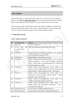
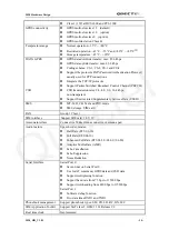
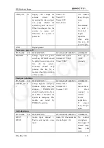
RI0 O
Ring
indicator
DCD0
O
Data carrier detection
VOLmax=0.34V
VOHmin=2.0V
VOHmax= VDD_EXT
connect RTS0
pin to GND
directly.
If unused keep
these pins
open.
Serial Port 1
RXD1 I
Receiving
data
TXD1 O
Transmitting
data
If unused keep
these pins
open.
RTS1
I
Request to send of serial
port1
CTS1
O
Clear to send of serial port1
These two
pins are
multiplex.
RTS1, CTS1
function is not
supported in
default
firmware and
need to be
customized if
require.
If unused keep
these pins
open.
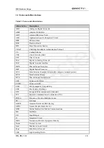
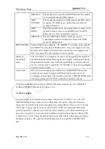
SIM interface
PIN NAME
I/O DESCRIPTION
DC CHARACTERISTICS COMMENT
SIM_VDD
O
Voltage supply for SIM card
The
voltage
can
be
selected by software
automatically, 1.8V or 3V
SIM_DATA I/O SIM
data
SIM_CLK O SIM
clock
SIM_RST O
SIM
reset
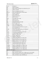
VIHmin=0.7*SIM_VDD
VOHmin=0.8*SIM_VDD
VOLmax=0.4V
When SIM_VDD=3V
VILmax=0.4V
When SIM_VDD=1.8V
VILmax=0.2* SIM_VDD
VOHmin=0.9*SIM_VDD
When SIM_VDD=3V
VOLmax=0.4V
When SIM_VDD=1.8V
VOLmax=0.2* SIM_VDD
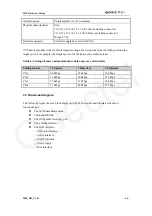
All signals of
SIM interface
should be
protected
against ESD
with a TVS
diode array.
Maximum
trace length
200mm from
the module
pin to SIM
card holder.
SIM_PRESE
NCE
I
SIM card detection. Pulled
down internally.
VILmax=0.67V
VIHmin=1.7V
If
SIM_PRESE
NCE goes
M20_HD_V1.01
- 21 -
Quectel


