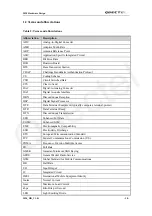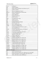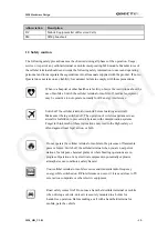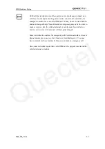
M20 Hardware Design
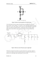
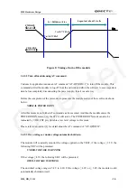
C2
C1
VBAT
+
C1=100µF, C2=0.1µF~1µF
Figure 2
: Reference bypass capacitors for the VBAT input
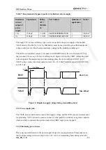
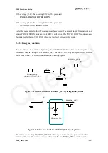
The circuit design of the power supply for the module largely depends on the power source.
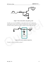
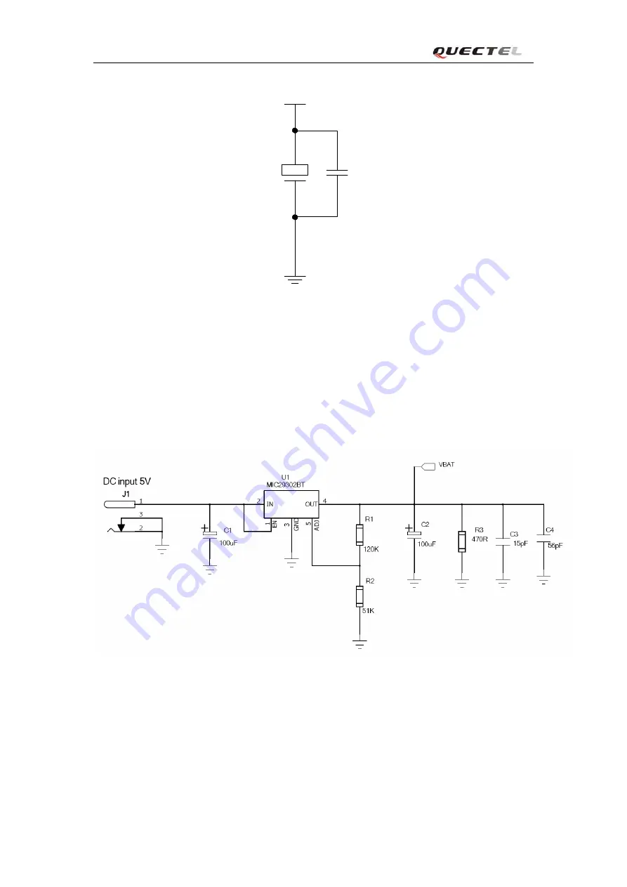
Figure 3 shows a reference design of +5V input power source. The designed output for the power
supply is 4.16V, thus a linear regulator can be used. If there’s a big voltage difference between the
input source and the desired output (VBAT), a switching converter power supply would be
preferable for its better efficiency especially with the 2A peak current in burst mode of the
module.
Figure 3
: Reference circuit of the source power supply input
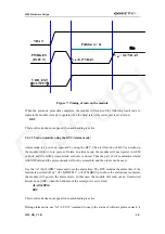
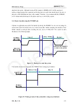
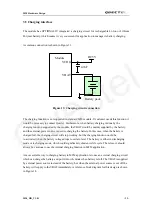
When the power supply for the module can’t provide current of 2A, proper bigger capacitor is
required so as to supply for the current demand during the burst transmission period. Reference
capacitors for corresponding limited current supply are listed in Table7.
M20_HD_V1.01
- 24 -
Quectel

