M20 Hardware Design
ACIN
VBAT
IR
GND
LDO
Charge IC
ACIN
VOUT
GND
ADJ
DC5V/2A
Module
VBAT
GND
PMOS
Batttery Pack
10K
100K
220uF
G
S
D
100nF
100uF
10uF
C1
100nF
C2
C3
R1
R3
R2
R4
R5
R6
D2
D1
U1
U2
C4
C5
Q1
4.3V~4.4V
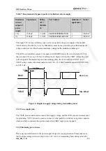
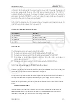
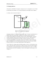
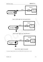
Figure 14: Reference external battery charging circuit
Figure 14 shows the reference battery charging circuit for M2M application. U1 is an LDO which
can supply current more than 2A and can output a voltage of 4.3~4.4V through adjusting the
resistance of R1 and R2. R3 is the minimum load which value can usually be found in the
datasheet of U1. Both D1 and D2 are Schottky barrier diodes, which is capable of forward current
more than 1.5A and has low forward voltage drop and fast switching feature. Q1 is a P-channel
MOSFET which acts as a switch between battery supply and external power supply. When the
external power supply is present, Q1 is cut off and the module is powered by external supply.
Otherwise, Q1 is turned on and the module is supplied by the battery. The Q1 P-channel MOSFET
must be able to supply continuous drain current bigger than 2A. Moreover, on-resistance of
Drain
−
to
−
Source should be as small as possible which means lower thermal power dissipation and
voltage drop. U2 is a charging IC, which should be chosen according to the requirements of the
application. Since the module is powered by external supply during most of the time in common
application, charging current of more than 100mA would be enough. Furthermore, the external 5V
DC power supply should be capable of supplying current more than the sum of maximum
charging current and maximum module load current, which is happened in GPRS 4 slots
transmission at highest power control level in GSM900MHz or GSM850MHz band.
3.5.1 Battery pack characteristics
The module has optimized the charging algorithm for the Li-Ion battery that meets the
M20_HD_V1.01
- 34 -
Quectel

