M20 Hardware Design
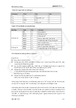
Table 18: Typical speaker output characteristic
Parameter
Min
Typ
Max
Unit
load
Resistance
28 32
Ω
Single
Ended
Ref level
0
2.4
Vpp
load
Resistance
28 32
Ω
Normal
Output(SPK1)
Differential
Ref level
0
4.8
Vpp
load
Resistance
16
32
Ω
Auxiliary
Output(SPK2)
Single
Ended
Ref level
0
2.4
Vpp
Maxim driving
current limit of
SPK1 and
SPK2
50
mA
3.10.4 DAI interface
(
optional
)
The module provides digital audio interface on the B2B connector. This interface can
communicate with external digital audio interface, such as BT, CODEC and only supports master
mode. Each pin definition of the DAI interface is listed in Table 19.
Table
19
:
Pin definition of the DAI interface
Interface
Name
Pin
Function
RXDDAI
7
Receive digital audio signal
TFSDAI
8
Frame synchronization signal
SCLK 9 Serial
bit
clock
DAI
TXDDAI
10
Transmit digital audio signal
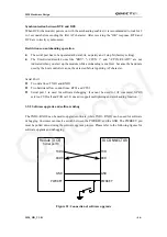
The SLCK clock signal is an output, generating a 256KHz bit clock as master. The TFSDAI frame
sync signal is an output, generating an 8KHz, and both long frame sync and short frame sync are
supported. The PCM interface can transmit 16-bit stereo or 32-bit mono 8 kHz sampling rate voice
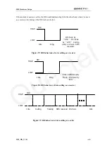
signal. Figure 32 shows the timing diagram of the DAI interface. Note that the serial data changes
when the clock is rising and is latched when the clock is falling.
M20_HD_V1.01
- 54 -
Quectel

