M20 Hardware Design
5.2 Absolute maximum ratings
The absolute maximum rating for power supply and voltage on digital and analog pins of module
are listed in the following table:
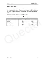
Table 32: Absolute maximum ratings
Parameter
Min
Max
Unit
VBAT 0
4.7
V
Peak current of power supply
0
2
A
RMS current of power supply (during one TDMA- frame)
0
0.7
A
Voltage at digit pins
-0.3
3.3
V
Voltage at analog pins
-0.3
3.0
V
Voltage at digit/analog pins in POWER DOWN mode
-0.25
0.25
V
5.3 Operating temperatures
The operating temperature is listed in the following table:
Table 33: Operating temperature
Parameter
Min
Typ
Max
Unit
Normal temperature
-35
25
80
℃
Restricted operation*
-45 to -35
80 to 85
℃
Storage temperature
-45
+90
℃
*
When the module works in this temperature range, the deviations from the GSM specification
may occur. For example, the frequency error or the phase error could increase.
5.4 Power supply ratings
Table 34: The module power supply ratings
Param
eter
Description
Conditions
Min
Typ
Ma
x
Unit
VBAT Supply voltage
Voltage must stay within the
min/max values, including
voltage drop, ripple, and spikes.
3.4 4.0
4.5 V
Voltage
drop
during
transmitting burst
Normal condition, power
control level for Pout max
400
mV
M20_HD_V1.01
- 66 -
Quectel

