GSM/GPRS/GNSS Module Series
MC60 Series Hardware Design
MC60_Series_Hardware_Design Confidential / Released 23 / 114
GNSS_
RXD
23
DI
Receive data
VOHnom=2.8V
VILmin=-0.3V
VILmax=0.7V
VIHmin=2.1V
VIHmax=3.1V
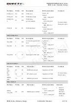
(U)SIM Interface
Pin Name
Pin No.
I/O
Description
DC Characteristics
Comment
SIM1_ VDD
SIM2_ VDD
18
13
PO
Power supply for
(U)SIM card
The voltage can be
selected by software
automatically. Either
1.8V or 3.0V.
All signals of
(U)SIM interface
should be
protected against
ESD with a TVS
diode array;
Maximum trace
length is 200mm
from the module
pad to (U)SIM
card connector.
SIM1_ CLK
SIM2_ CLK
19
10
DO
Clock signal of (U)SIM
card
V
OL
max=
0.15 × SIM_VDD
V
OH
min=
0.85 × SIM_VDD
SIM1_
DATA
SIM2_
DATA
21
11
IO
Data signal of (U)SIM
card
V
IL
max=
0.25 × SIM_VDD
V
IH
min=
0.75 × SIM_VDD
V
OL
max=
0.15 × SIM_VDD
V
OH
min=
0.85 × SIM_VDD
SIM1_ RST
SIM2_ RST
20
12
DO
Reset signal of (U)SIM
card
V
OL
max=
0.15 × SIM_VDD
V
OH
min=
0.85 × SIM_VDD
SIM_
GND
16
Specified ground for
(U)SIM card
SIM1_
PRESENCE
37
DI
(U)SIM1 card insertion
detection
V
IL
min=0V
V
IL
max=
0.25 × VDD_EXT
V
IH
min=
0.75×VDD_EXT
VIHmax=
0.2
ADC
Pin Name
Pin No.
I/O
Description
DC Characteristics
Comment
ADC
6
AI
General purpose
analog to digital
converter
Voltage range:
0V to 2.8V
If unused, keep
this pin open
Digital Audio Interface (PCM)
Quectel
Confidential

