Smart LTE Module Series
SC66 Hardware Design
SC66_Hardware_Design 43 / 139
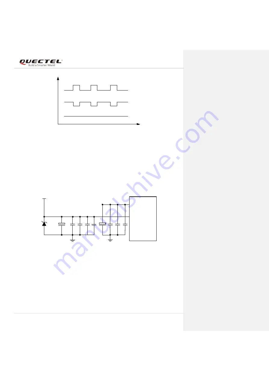
2.85V
Voltage
4.0V
Input current
3A
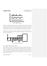
Figure 3: Voltage Drop Sample
To prevent the voltage from dropping below 2.85V, a bypass capacitor of about 100µF with low ESR
(ESR=0.7Ω) should be used, and a multi-layer ceramic chip capacitor (MLCC) array should also be
reserved due to its ultra-low ESR. It is recommended to use three ceramic capacitors (100nF, 33pF, 10pF)
for composing the MLCC array, and place these capacitors close to VBAT/VDD_RF pins. The width of
VBAT trace should be no less than 3mm. In principle, the longer the VBAT trace is, the wider it will be.
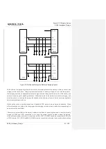
In addition, in order to get a stable power source, it is suggested to use a 0.5W TVS and place it as close
to the VBAT pins as possible to increase voltage surge withstand capability. The following figure shows
the structure of the power supply.
Module
VDD_RF
VBAT
VBAT
C1
100uF
C6
100nF
C7
33pF
C8
10pF
+
C2
100nF
C3
33pF
C4
10pF
D1
100uF
+
NM
C5
4.7uF
C9
NM
Figure 4: Structure of Power Supply
3.4.3. Reference Design for Power Supply
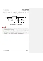
The power design for the module is very important, as the performance of module largely depends on the
power source. The power supply of SC66 should be able to provide sufficient current up to 3A at least. By
default, it is recommended to use a battery to supply power for SC66. But if battery is not intended to be
used, it is recommended to use a regulator for SC66. If the voltage difference between the input and
output is not too high, it is suggested to use an LDO to supply power for the module. If there is a big
voltage difference between the input source and the desired output (VBAT), a buck converter is preferred
to be used as the power supply.

