background image


  Smart  LTE Module  Series 

                                                                SC66  Hardware Design


SC66_Hardware_Design                                                                    73 / 139


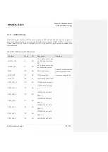
DSI1_ CLK_P

LEDA

NC

LEDK

NC (SDA-TP) 

VIO18

NC (VTP-TP) 

DSI1_LN3_P

LCD1_RST

DSI1_LN3_N

DSI1_LN2_P

DSI1_ CLK_N

DSI1_LN2_N

RESET

LCD_ID

NC (SCL-TP) 

NC (RST-TP) 

NC (EINT-TP) 

GND

VCC28

GND

MIPI_TDP3

MIPI_TDN3

GND

MIPI_TDP2

MIPI_TDN2

GND

MIPI_TDP1

MIPI_TDN1

GND

LDO3B_2P8

LDO11A_1P8

LCM1 _ LED+

LCM1 _LED-

1

2

3

4

5

6

7
8

9

10

12

13

14
15

16
17

18

19

20

21

22

23

24

25

26

27

MIPI_TDP0

MIPI_TDN0

GND

MIPI_TCP

MIPI_TCN

29

28

30

3

4

5

6

3

4

5

6

3

4

5

6

3

4

5

6

DSI1_LN1_N

DSI1_LN1_P

DSI1_LN0_N

DSI1_LN0_P

1

2

3

4

5

6

11

1

2

1

2

1

2

1

2

100nF

4.7uF

1uF

Module

LCM

FL1

FL2

FL3

FL4

FL5

EMI filter

C3

C2

C1

NC

GND

GND

GND
GND

ADC1

31

32
33

34

NC


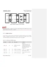
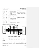
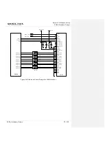
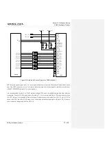
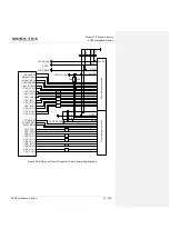
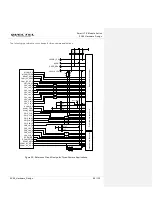
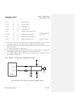
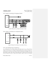
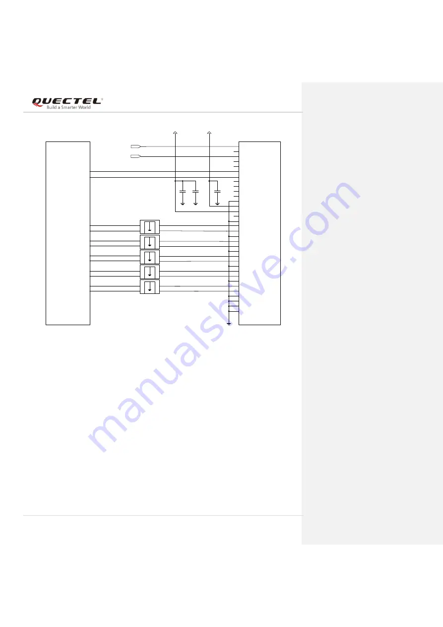
Figure 25: Reference Circuit Design for LCM1 Interface 


MIPI are high speed signal lines. It is recommended that common-mode filters should be added in series 

near the LCM connector, so as to improve protection against electromagnetic radiation interference. 

ICMEF112P900MFR using ICT is recommended. 


It is recommended to read the LCM ID register through MIPI when compatible design with other displays 

is required. If several LCM models share the same IC, it is recommended that LCM module factory burn 

the OTP register to distinguish different screens. Customers can also select the LCD_ID pin of LCM to 

connect the ADC pin of the SC66 module, but it should be noted that the output voltage of LCD_ID should 

not exceed the voltage range of the ADC pin. 


Summary of Contents for SC66

Page 1: ...SC66 Hardware Design Smart LTE Module Series Rev SC66_Hardware_Design_V1 0 Date 2019 08 13 Status Released www quectel com Model SC66 A ...

Page 2: ... THE INFORMATION PROVIDED IS BASED UPON CUSTOMERS REQUIREMENTS QUECTEL MAKES EVERY EFFORT TO ENSURE THE QUALITY OF THE INFORMATION IT MAKES AVAILABLE QUECTEL DOES NOT MAKE ANY WARRANTY AS TO THE INFORMATION CONTAINED HEREIN AND DOES NOT ACCEPT ANY LIABILITY FOR ANY INJURY LOSS OR DAMAGE OF ANY KIND INCURRED BY USE OF OR RELIANCE UPON THE INFORMATION ALL INFORMATION SUPPLIED HEREIN IS SUBJECT TO CH...

Page 3: ...Smart LTE Module Series SC66 Hardware Design SC66_Hardware_Design 2 139 About the Document History Revision Date Author Description 1 0 2019 08 13 Jian WU Chris ZHANG Initial ...

Page 4: ...rease Voltage Drop 42 3 4 3 Reference Design for Power Supply 43 3 5 Turn on and off Scenarios 45 3 5 1 Turn on the Module Using PWRKEY 45 3 5 2 Turn on the Module Automatically 47 3 5 3 Reboot Turn off the Module 47 3 6 VRTC Interface 48 3 7 Power Output 49 3 8 Battery Charge and Management 49 3 9 USB Interfaces 52 3 9 1 Type C Interface 52 3 9 1 1 USB Type C Mode 52 3 9 1 2 DisplayPort Mode 54 3...

Page 5: ...T Performance 92 5 GNSS 93 5 1 GNSS Performance 93 5 2 GNSS RF Design Guidelines 94 6 Antenna Interfaces 95 6 1 Main Rx diversity Antenna Interfaces 95 6 1 1 Main and Rx diversity Antenna Interfaces Reference Design 99 6 1 2 Reference Design of RF Layout 99 6 2 Wi Fi BT Antenna Interface 101 6 3 GNSS Antenna Interface 103 6 3 1 Recommended Circuit for Passive Antenna 104 6 3 2 Recommended Circuit ...

Page 6: ...p and Bottom View of the Module 132 9 Storage Manufacturing and Packaging 133 9 1 Storage 133 9 2 Manufacturing and Soldering 134 9 3 Packaging 135 10 Appendix A References 137 11 Appendix B GPRS Coding Schemes 140 12 Appendix C GPRS Multi slot Classes 141 13 Appendix D EDGE Modulation and Coding Schemes 143 ...

Page 7: ...E THE MODULE 64 TABLE 20 PIN DEFINITION OF GPIO INTERFACES 64 TABLE 21 PIN DEFINITION OF I2C INTERFACES 66 TABLE 22 PIN DEFINITION OF I2S INTERFACES 66 TABLE 23 PIN DEFINITION OF SPI INTERFACE 68 TABLE 24 PIN DEFINITION OF ADC INTERFACES 68 TABLE 25 PIN DEFINITION OF LCM INTERFACES 69 TABLE 26 PIN DEFINITION OF TOUCH PANEL INTERFACES 74 TABLE 27 PIN DEFINITION OF CAMERA INTERFACES 75 TABLE 28 TRAC...

Page 8: ...CONSUMPTION 116 TABLE 53 SC66 CE RF OUTPUT POWER 120 TABLE 54 SC66 A RF OUTPUT POWER 121 TABLE 55 SC66 J RF OUTPUT POWER 122 TABLE 56 SC66 E RF OUTPUT POWER 122 TABLE 57 SC66 CE RF RECEIVING SENSITIVITY 124 TABLE 58 SC66 A RF RECEIVING SENSITIVITY 125 TABLE 59 SC66 J RF RECEIVING SENSITIVITY 125 TABLE 60 SC66 E RF RECEIVING SENSITIVITY 126 TABLE 61 ESD CHARACTERISTICS TEMPERATURE 25 C HUMIDITY 45 ...

Page 9: ...N U SIM CARD CONNECTOR 62 FIGURE 21 REFERENCE CIRCUIT FOR SD CARD INTERFACE 63 FIGURE 22 LCM0 EXTERNAL BACKLIGHT DRIVER REFERENCE CIRCUIT 71 FIGURE 23 REFERENCE CIRCUIT DESIGN FOR LCM1 INTERFACE 71 FIGURE 24 REFERENCE CIRCUIT DESIGN FOR LCM0 INTERFACE 72 FIGURE 25 REFERENCE CIRCUIT DESIGN FOR LCM1 INTERFACE 73 FIGURE 26 REFERENCE CIRCUIT DESIGN FOR TP0 INTERFACE 75 FIGURE 27 REFERENCE CIRCUIT DESI...

Page 10: ... 104 FIGURE 44 REFERENCE CIRCUIT DESIGN FOR GNSS ACTIVE ANTENNA 105 FIGURE 45 DIMENSIONS OF THE U FL R SMT CONNECTOR UNIT MM 107 FIGURE 46 MECHANICALS OF U FL LP CONNECTORS 107 FIGURE 47 SPACE FACTOR OF MATED CONNECTOR UNIT MM 108 FIGURE 48 MODULE TOP AND SIDE DIMENSIONS 129 FIGURE 49 MODULE BOTTOM DIMENSIONS TOP VIEW 130 FIGURE 50 RECOMMENDED FOOTPRINT TOP VIEW 131 FIGURE 51 TOP VIEW OF THE MODUL...

Page 11: ...mitter module s are installed and operating The modules should be transmitting and the evaluation should confirm that the module s intentional emissions are compliant i e fundamental and out of band emissions The host manufacturer must verify that there are no additional unintentional emissions other than what is permitted in Part 15 Subpart B or emissions are complaint with the transmitter s rule...

Page 12: ... Rules These limits are designed to provide reasonable protection against harmful interference in a residential installation This equipment generates uses and can radiate radio frequency energy and if not installed and used in accordance with the instructions may cause harmful interference to radio communications However there is no guarantee that interference will not occur in a particular instal...

Page 13: ...e band 5725 5825 MHz shall comply with the e i r p limits specified for point to point and non point to point operation as appropriate L appareil peut interrompre automatiquement la transmission en cas d absence d informations à transmettre ou de panne opérationnelle Notez que ceci n est pas destiné à interdire la transmission d informations de contrôle ou de signalisation ou l utilisation de code...

Page 14: ... hardware interfaces which are connected with customers applications This document can help customers quickly understand module interface specifications electrical and mechanical details as well as other related information of SC66 module Associated with application note and user guide customers can use SC66 module to design and set up mobile applications easily ...

Page 15: ...consult the airline staff for more restrictions on the use of wireless devices on boarding the aircraft Wireless devices may cause interference on sensitive medical equipment so please be aware of the restrictions on the use of wireless devices when in hospitals clinics or other healthcare facilities Cellular terminals or mobiles operating over radio signals and cellular network cannot be guarante...

Page 16: ...Fi 802 11a b g n ac and BT5 0 standards Integrate GPS GLONASS BeiDou satellite positioning systems Support multiple audio and video codecs Built in high performance AdrenoTM GPU 512 graphics processing unit Provide multiple audio and video input output interfaces as well as abundant GPIO interfaces SC66 are available in six variants SC66 CE SC66 A SC66 J SC66 E SC66 W and SC66 MW The following tab...

Page 17: ...B12 B13 B14 B17 B25 B26 B66 B71 LTE TDD B41 WCDMA B2 B4 B5 Wi Fi 802 11a b g n ac 2402MHz 2482MHz 5180MHz 5825MHz BT 5 0 2402MHz 2480MHz GNSS GPS 1575 42MHz 1 023MHz GLONASS 1597 5MHz 1605 8MHz BeiDou 1561 098MHz 2 046MHz Type Frequency Bands LTE FDD B1 B3 B5 B8 B11 B18 B19 B21 B26 B28 A B LTE TDD B41 WCDMA B1 B6 B8 B19 Wi Fi 802 11a b g n ac 2402MHz 2482MHz 5180MHz 5825MHz BT 5 0 2402MHz 2480MHz ...

Page 18: ...20 B28 A B LTE TDD B38 B39 B40 B41 WCDMA B1 B2 B4 B5 B8 GSM 850 900 1800 1900MHz Wi Fi 802 11a b g n ac 2402MHz 2482MHz 5180MHz 5825MHz BT 5 0 2402MHz 2480MHz GNSS GPS 1575 42MHz 1 023MHz GLONASS 1597 5MHz 1605 8MHz BeiDou 1561 098MHz 2 046MHz Type Frequency Bands LTE FDD LTE TDD WCDMA TD SCDMA CDMA GSM Wi Fi 802 11a b g n ac 2402MHz 2482MHz 5180MHz 5825MHz BT 5 0 2402MHz 2480MHz GNSS ...

Page 19: ...ncluding 152 LCC pads and 172 LGA pads With a compact profile of 43 0mm 44 0mm 2 85mm SC66 can meet almost all requirements for M2M applications such as smart metering smart home security routers wireless POS mobile computing devices PDA phone tablet PC and etc Besides SC66 supports AI applications such as face recognition and vehicle recognition Type Frequency Bands LTE FDD LTE TDD WCDMA TD SCDMA...

Page 20: ...age 3 55V 4 4V Typical 4 0V Transmitting Power Class 4 33dBm 2dB for GSM850 EGSM900 Class 1 30dBm 2dB for DCS1800 PCS1900 Class E2 27dBm 3dB for GSM850 EGSM900 8 PSK Class E2 26dBm 3dB for DCS1800 PCS1900 8 PSK Class 3 24dBm 1 3dB for WCDMA bands Class 3 24dBm 3 1dB for EVDO CDMA BC0 Class 2 24dBm 1 3dB for TD SCDMA bands Class 3 23dBm 2dB for LTE FDD bands Class 3 23dBm 2dB for LTE TDD bands LTE ...

Page 21: ...chemes CS 1 4 and MCS 1 9 Max 296Kbps DL 236 8Kbps UL WLAN Features 2 4GHz 5GHz support 802 11a b g n ac maximally up to 433Mbps Support AP and STA mode Bluetooth Features BT5 0 GNSS Features GPS GLONASS BeiDou SMS Text and PDU mode Point to point MO and MT SMS cell broadcast LCM Interfaces 2560 1600 60fps primary display 4k 30fps over DP Dual MIPI DSI Camera Interfaces Support three groups of 4 l...

Page 22: ...rface Support SD 3 0 Support SD card hot plug U SIM Interfaces 2 U SIM interfaces Support USIM SIM card 1 8V 2 95V Support Dual SIM Dual Standby supported by default I2C Interfaces Support up to 5 I2C interfaces used for peripherals such as TP camera sensor etc I2S Interfaces 2 I2S interfaces ADC Interfaces 2 general purpose ADC interfaces SPI Interface 1 SPI interface only support master mode Rea...

Page 23: ...ht reduce in their value and exceed the specified tolerances When the temperature returns to the normal operating temperature levels the module will meet 3GPP specifications again 3 means under development 2 3 Functional Diagram The following figure shows a block diagram of SC66 and illustrates the major functional parts Power management Radio frequency Baseband LPDDR4X eMMC flash Peripheral inter...

Page 24: ...LDO14A_1P8 BATTERY VPH_PWR VBUS GPIOs 13 2 769 I2C I2S PWRKEY VOL DOWN PM660L SD_PU_VDD SD_VDD ADCs LDO7B_3P125 LDO3B_2P8 HK ADC PM660 PWM PM 3003A 0Ω FEM ANT_WIFI_MIMO VPH_PWR 5G TX 5G TX 5G RX PDET 2 4G TRX 5G RX PDET 2 4G TRX Figure 1 Functional Diagram The red dotted frame is Wi Fi MIMO path which is not supported by SC66 CE and SC66 W 2 4 Evaluation Board In order to help customers design and...

Page 25: ... chapters provide the detailed description of pins interfaces listed below Power supply Turn on and off function VRTC interface Power Output Charging interface USB interfaces UART interfaces U SIM interfaces SD card interface GPIO interfaces I2C interfaces I2S interfaces SPI interface ADC interfaces LCM interfaces TP touch panel interfaces Camera interfaces Sensor interfaces Audio interfaces Emerg...

Page 26: ...5 56 57 58 59 60 61 62 63 64 323 321 322 24 25 26 27 29 28 30 31 32 33 34 35 36 37 38 65 66 67 68 69 70 71 72 73 74 75 76 77 78 79 80 81 82 83 84 85 86 87 88 89 90 91 92 93 94 95 96 97 98 99 100 101 102 103 104 105 106 107 109 111 112 113 114 115 116 117 118 120 121 122 123 124 125 126 128 129 130 131 132 133 134 135 136 137 138 139 141 142 143 144 145 146 147 148 149 150 151 152 127 140 153 154 1...

Page 27: ...gital output IO Bidirectional OD Open drain PI Power input PO Power output Power Supply Pin Name Pin No I O Description DC Characteristics Comment VBAT 36 37 38 PI PO Power supply for the module Vmax 4 4V Vmin 3 55V Vnorm 4 0V It must be provided with sufficient current up to 3 0A It is suggested to use a TVS to increase voltage surge withstand capability VDD_RF 1 2 PO Connect to external bypass c...

Page 28: ...5V IOmax 150mA Power supply only for DP switch LDO11A_1P8 10 PO 1 8V output power supply Vnorm 1 8V IOmax 150mA Power supply for I O VDD of cameras LCDs and TP etc LDO14A_1P8 158 PO 1 8V output power supply Vnorm 1 8V IOmax 150mA Power supply for I O VDD of sensors LDO3B_2P8 12 PO 2 8V output power supply Vnorm 2 8V IOmax 600mA Power supply for sensor and LCM VPH_PWR 30 PO VBAT output power supply...

Page 29: ...his pin to the ground MIC2_P 46 AI Microphone input for headset Headset microphone input MIC3_P 169 AI Microphone input for secondary microphone Secondary microphone input EAR_P 53 AO Earpiece output EAR_M 52 AO Earpiece output SPK_P 55 AO Speaker output SPK_M 54 AO Speaker output HPH_R 51 AO Headphone right channel output HPH_REF 50 AI Headphone reference ground It should be connected to main GND...

Page 30: ...TG Support software download USB1_HS_DP 32 IO USB 2 0 differential data bus USB_SS2_TX _P 165 IO USB 3 1 channel 2 differential transmit 90Ω differential impedance USB 3 1 standard compliant USB_SS2_TX _M 164 IO USB 3 1 channel 2 differential transmit USB_SS2_RX _P 162 IO USB 3 1 channel 2 differential receive USB_SS2_RX _M 161 IO USB 3 1 channel 2 differential receive USB_SS1_RX _P 171 IO USB 3 1...

Page 31: ... SS_DIR_IN 21 DI CC status detection pin When USB Type C is used it should be connected to SS_DIR_OUT When uUSB is used it should be connected to GND Cannot be multiplexed into a general purpose GPIO SS_DIR_OUT 226 DO CC status output pin U SIM Interfaces Pin Name Pin No I O Description DC Characteristics Comment USIM1_DET 145 DI U SIM1 card hot plug detection VILmax 0 63V VIHmin 1 17V Active Low ...

Page 32: ...LK 208 DO U SIM2 card clock signal VOLmax 0 4V VOHmin 0 8 USIM2_VDD USIM2_DATA 209 IO U SIM2 card data signal VILmax 0 2 USIM2_VDD VIHmin 0 7 USIM2_VDD VOLmax 0 4V VOHmin 0 8 USIM2_VDD USIM2_VDD 210 PO U SIM2 card power supply Either 1 8V or 2 95V U SIM card is supported UART Interfaces Pin Name Pin No I O Description DC Characteristics Comment DEBUG_TXD 5 DO DEBUG UART transmit data VOLmax 0 45V ...

Page 33: ...d digital clock signal of SD card 1 8V SD card VOLmax 0 45V VOHmin 1 4V 2 95V SD card VOLmax 0 36V VOHmin 2 13V SD_CMD 69 IO Command signal of SD card 1 8V SD card VILmax 0 58V VIHmin 1 27V VOLmax 0 45V VOHmin 1 4V 2 95V SD card VILmax 0 73V VIHmin 1 85V VOLmax 0 36V VOHmin 2 13V SD_DATA0 68 IO High speed bidirectional digital signal lines of SD card SD_DATA1 67 IO SD_DATA2 66 IO SD_DATA3 65 IO SD...

Page 34: ...anel TP1 TP1_I2C_SDA 204 OD I2C data signal of touch panel TP1 LCM Interfaces Pin Name Pin No I O Description DC Characteristics Comment PWM 152 DO PWM signal output The voltage is equal to VBAT voltage Cannot be multiplexed into a general purpose GPIO LCD0_RST 127 DO LCD0 reset signal VOLmax 0 45V VOHmin 1 35V 1 8V power domain It should not be pulled up LCD0_TE 126 DI LCD0 tearing effect signal ...

Page 35: ... 113 DO LCD1 reset signal VOLmax 0 45V VOHmin 1 35V 1 8V power domain DSI1_CLK_N 103 LCD1 MIPI clock signal 85Ω differential impedance DSI1_CLK_P 102 LCD1 MIPI clock signal DSI1_LN0_N 105 LCD1 MIPI lane 0 data signal 85Ω differential impedance DSI1_LN0_P 104 LCD1 MIPI lane 0 data signal DSI1_LN1_N 107 LCD1 MIPI lane 1 data signal 85Ω differential impedance DSI1_LN1_P 106 LCD1 MIPI lane 1 data sign...

Page 36: ...r camera 85Ω differential impedance CSI1_LN0_P 90 AI MIPI lane 0 data signal of rear camera CSI1_LN1_N 93 AI MIPI lane 1 data signal of rear camera 85Ω differential impedance CSI1_LN1_P 92 AI MIPI lane 1 data signal of rear camera CSI1_LN2_N 95 AI MIPI lane 2 data signal of rear camera 85Ω differential impedance CSI1_LN2_P 94 AI MIPI lane 2 data signal of rear camera CSI1_LN3_N 97 AI MIPI lane 3 d...

Page 37: ... Can be multiplexed into differential data of the fourth camera CSI2_LN2_P 189 AI MIPI lane 2 data signal of depth camera 85Ω differential impedance Can be multiplexed into differential data of the fourth camera CSI2_LN3_N 192 AI MIPI lane 3 data signal of depth camera 85Ω differential impedance Can be multiplexed into differential clock of the fourth camera CSI2_LN3_P 191 AI MIPI lane 3 data sign...

Page 38: ...PI lane 3 data signal of front camera MCAM_MCLK 99 DO Master clock signal of rear camera VOLmax 0 45V VOHmin 1 35V 1 8V power domain SCAM_MCLK 100 DO Master clock signal of front camera 1 8V power domain MCAM_RST 74 DO Reset signal of rear camera 1 8V power domain MCAM_PWDN 73 DO Power down signal of rear camera 1 8V power domain SCAM_RST 72 DO Reset signal of front camera 1 8V power domain SCAM_P...

Page 39: ...NSOR_I2C Interfaces Pin Name Pin No I O Description DC Characteristics Comment SENSOR_I2C_ SCL 131 OD I2C clock signal of external sensors 1 8V power domain Cannot be multiplexed into general purpose GPIOs SENSOR_I2C_ SDA 132 OD I2C data signal of external sensors Sensor Interfaces Pin Name Pin No I O Description DC Characteristics Comment ACCL_INT 252 IO Interrupt signal of proximity sensor 1 8V ...

Page 40: ...O 324 AI AO Wi Fi MIMO antenna interface 50Ω impedance SC66 CE and SC66 W do not support this function FM_ANT 244 AI FM antenna interface FM function is still under development GPIO Interfaces Pin Name Pin No I O Description DC Characteristics Comment GPIO_21 231 IO GPIO VILmax 0 63V VIHmin 1 17V VOLmax 0 45V VOHmin 1 35V 1 8V power domain GPIO_34 236 IO GPIO 1 8V power domain GPIO_40 238 IO GPIO ...

Page 41: ... 1 8V power domain GPIO_13A 233 IO GPIO 1 8V power domain GRFC Interfaces Pin Name Pin No I O Description DC Characteristics Comment GRFC_19 242 IO GRFCDedicated GPIO Only for RF debug It should not be pulled up Cannot be multiplexed into general purpose GPIOs GRFC_18 241 IO SPI Interface Pin Name Pin No I O Description DC Characteristics Comment SPI3_CS 201 DO Chip selection signal 1 8V power dom...

Page 42: ...t LPI_MI2S_ DATA0 154 IO LPI_I2S signal data0 LPI_MI2S_ DATA1 155 IO LPI_I2S signal data1 Emergency Download Interface Pin Name Pin No I O Description DC Characteristics Comment USB_BOOT 57 DI Force the module to enter emergency download mode Pulled up to LDO13A_1P8 during power up will force the module to enter emergency download mode Other Interfaces Pin Name Pin No I O Description DC Characteri...

Page 43: ... performance such as load capacity voltage ripple etc directly influences the module s performance and stability Under ultimate conditions the module may have a transient peak current up to 3A If the power supply capability is not sufficient there will be voltage drops and if the voltage drops below 2 85V the module will be powered off automatically Therefore please make sure the input voltage wil...

Page 44: ... possible to increase voltage surge withstand capability The following figure shows the structure of the power supply Module VDD_RF VBAT VBAT C1 100uF C6 100nF C7 33pF C8 10pF C2 100nF C3 33pF C4 10pF D1 100uF NM C5 4 7uF C9 NM Figure 4 Structure of Power Supply 3 4 3 Reference Design for Power Supply The power design for the module is very important as the performance of module largely depends on...

Page 45: ...ircuit of Power Supply 1 It is recommended to switch off the power supply when the module is in abnormal state and then switch on the power to restart the module 2 The module supports battery charging function by default If the above power supply design is adopted please make sure the charging function is disabled by software or connect VBAT to Schottky diode in series to avoid the reverse current...

Page 46: ...r driver to control the PWRKEY A simple reference circuit is illustrated in the following figure Turn on pulse PWRKEY 4 7K 47K 3ms R1 R2 Q1 R3 1K Figure 6 Turn on the Module Using Driving Circuit Another way to control the PWRKEY is using a button directly For ESD protection A TVS component placed near the button and a 1kΩ resistor connected to the PWRKEY in series are indispensable A reference ci...

Page 47: ...ing figure VBAT Typ 4 0V PWRKEY 3ms Others LDO13A_1P8 LDO11A_1P8 Software controlled LDO14A_1P8 Active LDO7B_3P125 Software controlled Figure 8 Timing of Turning on Module Make sure that VBAT is stable before pulling down PWRKEY pin The recommended time between them is no less than 30ms PWRKEY cannot be pulled down all the time NOTE ...

Page 48: ... module is turned on automatically through CBL_PWR_N then it cannot be turned off unless the battery is removed 3 5 3 Reboot Turn off the Module Pull down PWRKEY for at least 1s and then choose to turn off or reboot the module when the prompt window comes up Another way to reboot the module is to drive PWRKEY to a low level for at least 8s The restart scenario is illustrated in the following figur...

Page 49: ...e circuit design is shown VRTC 0R 100nF BAT Figure 11 RTC Powered by a Rechargeable Button Cell Battery 1 When VBAT is disconnected the recommended input voltage range for VRTC is 2 1V 3 25V and the recommended typical value is 3 0V 2 When powered by VBAT the RTC error is 100ppm When powered by VRTC the RTC error is about 200ppm 3 If a rechargeable battery is used the ESR of battery should be less...

Page 50: ...ickle charging pre charge constant current charging and constant voltage charging modes which optimize the charging procedure for Li ion and Li polymer batteries Trickle charging When the battery voltage is below 2 1V a 45mA trickle charging current is applied to the battery Pre charge When the battery voltage is charged up and is between 2 4V and 3 0V the maximum pre charge voltage is 2 4V 3 0V p...

Page 51: ...ng power input Power supply output for OTG device USB charger insertion detection Vmax 10V Vmin 3 6V Vnorm 5 0V VBAT 36 37 38 PI PO Power supply for the module Vmax 4 4V Vmin 3 55V Vnorm 4 0V BAT_PLUS 27 AI Differential input signal of battery voltage detection Must be connected BAT_MINUS 28 AI Differential input signal of battery voltage detection Must be connected BAT_THERM 29 AI Battery tempera...

Page 52: ... the battery and across a broad range of operating conditions It effectively protects the battery from over discharging and also allows users to estimate the battery life based on the battery level so as to timely save important data before completely power down Mobile devices such as mobile phones and handheld POS systems are powered by batteries When different batteries are utilized the charging...

Page 53: ...bps modes These USB interfaces can be used for AT command transmission data transmission software debugging and software upgrading 3 9 1 Type C Interface 3 9 1 1 USB Type C Mode The Type C interface has one USB 2 0 compliant high speed differential data pair USB1_HS_DP M and two USB 3 1 compliant super speed differential data pairs USB_SS1_RX_P M USB_SS1_TX_P M and USB_SS2_RX_P M USB_SS2_TX_P M Wh...

Page 54: ... 164 AO USB 3 1 channel 2 differential transmit USB_SS2_TX_P 165 AO USB 3 1 channel 2 differential transmit UUSB_TYPEC 23 DI uUSB USB Type C configuration selection pin When USB Type C is used it should be connected to VPH_PWR through a 10KΩ resistor When uUSB is used it should be connected to GND through a 10KΩ resistor Cannot be multiplexed into a general purpose GPIO USB_CC2 223 AI USB Type C c...

Page 55: ...Port Mode SC66 supports DisplayPort mode with 4 lanes up to 4K 30ps over USB Type C The DisplayPort mode and USB Type C mode cannot operate simultaneously In the DisplayPort Mode USB2 0 can be supported simultaneously and USB 3 1 cannot be supported simultaneously The pin descriptions in USB Type C DisplayPort mode is listed below Table 13 Pin Descriptions in USB DisplayPort Mode Cannot be multipl...

Page 56: ...LDO7B_3P125 DP_AUX_P DP_AUX_N LDO7B_3P125 100K 100K GPIO_76 LDO13A_1P8 0 1uF 0 1uF Module 100R 100MHZ 1UF GPIO_21 SBU1 SBU2 2 2K SGM7227YMS10G TR Figure 14 DisplayPort Reference Design 3 9 2 Micro USB Interface SC66 supports USB Type C interface by default Micro USB can be used via software configuration Micro USB interface can be supported through USB1_HS_DP M or USB2_HS_DP M Micro USB interface ...

Page 57: ...The reference circuit of Host mode configured by USB2 USB2_HS_DP USB2_HS_DM Module DP DM VBUS ID GND 100nF 4 7uF AW3605DNR SW VIN EN VOUT VOUT NC GPIO_15 1UH VPH_PWR 10uF 1uF GND 10K USB2_VBUS USB2_VBUS Pin Name Pin No I O Description Comment USB1_HS_DM 33 IO USB 2 0 differential data bus USB 2 0 standard compliant Support OTG USB1_HS_DP 32 IO USB 2 0 differential data bus USB2_HS_DM 25 IO USB 2 0...

Page 58: ... following principles while designing USB interface Pin No Signal Length mm Length Difference DP DM 32 USB1_HS_DP 46 15 1 20 33 USB1_HS_DM 44 95 171 USB_SS1_RX_P 39 75 0 00 172 USB_SS1_RX_M 39 75 174 USB_SS1_TX_P 35 75 0 00 175 USB_SS1_TX_M 35 75 162 USB_SS2_RX_P 31 6 0 16 161 USB_SS2_RX_M 31 6 165 USB_SS2_TX_P 37 7 0 40 164 USB_SS2_TX_M 37 3 26 USB2_HS_DP 40 75 0 20 25 USB2_HS_DM 40 95 221 DP_AUX...

Page 59: ... 90db otherwise the RF signal will be seriously affected Make sure the trace length difference between USB 3 1 RX and USB 3 1 TX differential pairs do not exceed 0 7mm Make sure the trace length difference between USB 2 0 DP and USB 2 0 DM differential pairs do not exceed 2mm For USB 3 1 the spacing between Rx and Tx signal traces should be three times the signal trace width The spacing between US...

Page 60: ...evel Translator Chip for UART6 The following figure is an example of connection between SC66 and PC A voltage level translator and a RS 232 level translator chip are recommended to be added between the module and PC as shown below data DEBUG_RXD 6 DI DEBUG UART receive data 1 8 power domain UART1_TXD 7 DO UART1 transmit data 1 8 power domain UART1_RXD 8 DI UART1 receive data 1 8 power domain UART6...

Page 61: ...2 3 11 U SIM Interfaces SC66 provides two U SIM interfaces which both meet ETSI and IMT 2000 requirements Dual SIM Dual Standby is supported by default Both 1 8V and 2 95V U SIM cards are supported and the U SIM interfaces are powered by the dedicated low dropout regulators in SC66 module Table 17 Pin Definition of U SIM Interfaces Pin Name Pin No I O Description Comment USIM1_DET 145 DI U SIM1 ca...

Page 62: ...o need to use USIM_DET please keep it open The following is a reference circuit for U SIM interface with a 6 pin U SIM card connector Cannot be multiplexed into a general purpose GPIO USIM1_VDD 141 PO U SIM1 card power supply Either 1 8V or 2 95V U SIM card is supported USIM2_DET 256 DI U SIM2 card insertion detection Active low Need external pull up to1 8V If unused keep this pin open USIM2_RST 2...

Page 63: ... should be placed near to U SIM card To avoid cross talk between USIM_DATA and USIM_CLK keep them away from each other and shield them with ground USIM_RST also needs ground protection In order to offer good ESD protection it is recommended to add a TVS diode array with parasitic capacitance not exceeding 50pF The 22Ω resistors should be added in series between the module and U SIM card so as to s...

Page 64: ...idth is 0 5mm or above In order to ensure the stability of drive power a 1uF and a 33pF capacitor should be added in parallel near the SD card connector CMD CLK DATA0 DATA1 DATA2 and DATA3 are all high speed signal lines In PCB design please control the characteristic impedance of them as 50Ω and do not cross them with other traces It is recommended to route the trace on the inner layer of PCB and...

Page 65: ...ould be 1 5 times the line width The capacitive reactance of data signal line should be 8 pF Table 19 SD Card Signal Trace Length Inside the Module 3 13 GPIO Interfaces SC66 has abundant GPIO interfaces with power domain of 1 8V The pin definition is listed below Table 20 Pin Definition of GPIO Interfaces Pin No Signal Length mm 70 SD_CLK 24 35 69 SD_CMD 24 30 68 SD_DATA0 24 30 67 SD_DATA1 24 30 6...

Page 66: ...pukp Wakeup GPIO_55 178 GPIO_55 B PD nppukp Wakeup GPIO_56 177 GPIO_56 B PD nppukp Wakeup GPIO_72 239 GPIO_72 B PD nppukp Wakeup GPIO_73 59 GPIO_73 B PD nppukp Wakeup GPIO_74 58 GPIO_74 B PD nppukp Wakeup GPIO_76 232 GPIO_76 B PD nppukp Wakeup GPIO_77 240 GPIO_77 B PD nppukp Wakeup GPIO_12 228 GPIO_12 B PD nppukp GPIO_13 227 GPIO_13 B PD nppukp Wakeup GPIO_14 230 GPIO_14 B PD nppukp GPIO_15 229 GP...

Page 67: ...terfaces Pin Name Pin No I O Description Comment TP0_I2C_SCL 140 OD TP I2C clock Used for TP0 TP0_I2C_SDA 206 OD TP I2C data CAM_I2C_SCL0 75 OD CAM I2C clock Used for rear and front camera CAM_I2C_SDA0 76 OD CAM I2C data CAM_I2C_SCL1 196 OD CAM I2C clock Used for depth camera CAM_I2C_SDA1 197 OD CAM I2C data SENSOR_I2C_SCL 131 OD Sensor I2C clock Used for sensor Cannot be multiplexed into general ...

Page 68: ...251 IO I2S serial data1 channel MI2S_2_MCLK 114 DO I2S main clock LPI_MI2S_SCLK 212 DO LPI_I2S serial clock signal Cannot be multiplexed into general purpose GPIOs LPI_MI2S_WS 156 DO LPI_I2S word select LPI_MI2S_DATA0 154 IO LPI_I2S signal data0 LPI_MI2S_DATA1 155 IO LPI_I2S signal data1 ...

Page 69: ...ow Table 24 Pin Definition of ADC Interfaces The resolution of the ADC is up to 15 bits Pin Name Pin No I O Description Comment SPI3_MOSI 248 DO Master out slave in of SPI interface SPI3_MISO 247 DI Master in salve out of SPI interface SPI3_CS 201 DO Chip selection signal of SPI interface SPI3_CLK 200 DO Clock signal of SPI interface Pin Name Pin No I O Description Comment ADC0 151 AI Universal AD...

Page 70: ... O Description Comment LDO11A_1P8 10 PO 1 8V output power supply for LCM logic circuit and DSI LDO3B_2P8 12 PO 2 8V output power supply for LCM analog circuits PWM 152 DO PWM signal output Cannot be multiplexed into a general purpose GPIO LCD0_RST 127 DO LCD0 reset signal It should not be pulled up LCD0_TE 126 DI LCD0 tearing effect signal DSI0_CLK_N 116 AO LCD0 MIPI clock signal DSI0_CLK_P 115 AO...

Page 71: ...AO LCD1 MIPI clock signal DSI1_LN0_N 105 AO LCD1 MIPI lane 0 data signal DSI1_LN0_P 104 AO LCD1 MIPI lane 0 data signal DSI1_LN1_N 107 AO LCD1 MIPI lane 1 data signal DSI1_LN1_P 106 AO LCD1 MIPI lane 1 data signal DSI1_LN2_N 109 AO LCD1 MIPI lane 2 data signal DSI1_LN2_P 108 AO LCD1 MIPI lane 2 data signal DSI1_LN3_N 111 AO LCD1 MIPI lane 3 data signal DSI1_LN3_P 110 AO LCD1 MIPI lane 3 data signa...

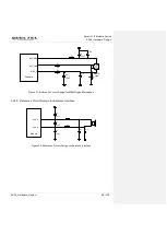
Page 72: ...ternal backlight drive circuit is shown in the figure below in which pins PWM Pin 152 Pin 238 can be used for backlight brightness adjustment LCM0 _LED Module 2 2uF Backlight Driver LCM0_LED VPH_PWR C1 PWM Figure 22 LCM0 External Backlight Driver Reference Circuit LCM1 _LED Module 2 2uF Backlight Driver LCM1_LED VPH_PWR C1 GPIO_40 Figure 23 Reference Circuit Design for LCM1 Interface GPIO_40 238 D...

Page 73: ... GND MIPI_TDP2 MIPI_TDN2 GND MIPI_TDP1 MIPI_TDN1 GND LDO3B_2P8 LDO11A_1P8 LCM0 _ LED LCM0 _LED 1 2 3 4 5 6 7 8 9 10 12 13 14 15 16 17 18 19 20 21 22 23 24 25 26 27 MIPI_TDP0 MIPI_TDN0 GND MIPI_TCP MIPI_TCN 29 28 30 3 4 5 6 3 4 5 6 3 4 5 6 3 4 5 6 DSI0_LN1_N DSI0_LN1_P DSI0_LN0_N DSI0_LN0_P 1 2 3 4 5 6 11 1 2 1 2 1 2 1 2 100nF 4 7uF 1uF Module LCM FL1 FL2 FL3 FL4 FL5 EMI filter C3 C2 C1 NC GND GND ...

Page 74: ...FL2 FL3 FL4 FL5 EMI filter C3 C2 C1 NC GND GND GND GND ADC1 31 32 33 34 NC Figure 25 Reference Circuit Design for LCM1 Interface MIPI are high speed signal lines It is recommended that common mode filters should be added in series near the LCM connector so as to improve protection against electromagnetic radiation interference ICMEF112P900MFR using ICT is recommended It is recommended to read the ...

Page 75: ... I O Description Comment LDO11A_1P8 10 PO 1 8V output power supply Pull up power supply of I2C Vnorm 1 8V IOmax 300mA LDO3B_2P8 12 PO 2 8V output power supply for TP TP power supply Vnom 2 8V Iomax 600mA TP0_INT 139 DI Interrupt signal of touch panel TP0 TP0_RST 138 DO Reset signal of touch panel TP0 TP0_I2C_SCL SCL 140 OD I2C clock signal of touch panel TP0 TP0_I2C_SDA 206 OD I2C data signal of t...

Page 76: ... Interfaces Based on standard MIPI CSI input interface SC66 module supports 3 cameras 4 lane 4 lane 4 lane or 4 cameras 4 lane 4 lane 2 lane 1 lane with maximum pixels up to 24MP for SC66 The video and photo quality are determined by various factors such as camera sensor camera lens quality etc Table 27 Pin Definition of Camera Interfaces Pin Name Pin No I O Description Comment GPIO_08B 13 DO Rear...

Page 77: ...ignal of front camera CSI0_LN3_N 86 AI MIPI lane 3 data signal of front camera CSI0_LN3_P 85 AI MIPI lane 3 data signal of front camera CSI1_CLK_N 89 AI MIPI clock signal of rear camera CSI1_CLK_P 88 AI MIPI clock signal of rear camera CSI1_LN0_N 91 AI MIPI data0 signal of rear camera CSI1_LN0_P 90 AI MIPI data0 signal of rear camera CSI1_LN1_N 93 AI MIPI data 1 signal of rear camera CSI1_LN1_P 92...

Page 78: ... MIPI lane 3 data signal of depth camera CSI2_LN3_P 191 AI MIPI lane 3 data signal of depth camera MCAM_MCLK 99 DO Rear camera clock signal SCAM_MCLK 100 DO Front camera clock signal DCAM_MCLK 194 DO Depth camera clock signal MCAM_RST 74 DO Rear camera reset signal SCAM_RST 72 DO Front camera reset signal DCAM_RST 180 DO Depth camera reset signal MCAM_PWDN 73 DO Rear camera PWDN signal SCAM_PWDN 7...

Page 79: ...uF LDO_IC VPH_PWR C1 GPIO_08B R1 100K C2 AVDD Module 2 2uF LDO_IC VPH_PWR C5 GPIO_04B R3 100K C6 DVDD_FRONT Module 2 2uF LDO_IC VPH_PWR C3 R2 100K C4 GPIO_5B Figure 27 Reference Circuit Design for Dual Camera Applications The following is a reference circuit design for dual camera applications ...

Page 80: ...ront camera connector 4 7uF 1uF 1uF MCAM_RST EMI EMI EMI EMI EMI EMI EMI EMI EMI EMI AVDD DVDD DOVDD 1uF CSI1_LN0_P CSI1_LN0_N CSI1_LN1_P CSI1_LN1_N CSI1_LN2_P CSI1_LN2_N CSI1_LN3_P CSI1_LN3_N CSI0_LN0_P CSI0_LN0_N CSI0_LN1_P CSI0_LN1_N CSI0_LN2_P CSI0_LN2_N CSI0_LN3_P CSI0_LN3_N DVDD 1uF 4 7uF 4 7uF AVDD DOVDD AVDD LDO3B_2P8 DVDD_REAR LDO11A_1P8 AFVDD DVDD_FRONT Figure 28 Reference Circuit Design...

Page 81: ...CAM_RST SCAM_ PWDN SCAM_MCLK CSI2_CLK_P CSI2_CLK_N CSI2_LN0_P CSI2_LN0_N CSI0_LN1_P CSI0_LN1_N CSI0_LN0_P CSI0_LN0_N CSI1_CLK_P CSI1_CLK_N CSI0_CLK_P CSI0_CLK_N AVDD 2 2K 2 2K Front camera connector 1uF 4 7 uF 4 7uF 1uF 1u F 4 7uF MCAM_RST DCAM_PWDN DCAM_MCLK DCAM_I2C_SDA1 DCAM_I2C_SCL1 DCAM_RST Depth camera connector LDO3B_1P8 EMI EMI EMI EMI EMI EMI EMI EMI DVDD_REAR 1uF 2 2K 2 2K DVDD EMI EMI 4...

Page 82: ... MIPI traces should keep the same length Be assure the reference ground plane for CSI DSI is complete and integral without any cut or void Route the camera CLK signal in the inner layer of the PCB between ground fills Route CSI and DSI traces according to the following rules a The intra pair spacing should be one time the trace width b The inter pair spacing should be 1 5 times the trace width c T...

Page 83: ...0 00 104 DSI1_LN0_P 28 00 107 DSI1_LN1_N 30 00 0 00 106 DSI1_LN1_P 30 00 109 DSI1_LN2_N 33 50 0 00 108 DSI1_LN2_P 33 50 111 DSI1_LN3_N 37 50 0 00 110 DSI1_LN3_P 37 50 89 CSI1_CLK_N 16 00 0 00 88 CSI1_CLK_P 16 00 91 CSI1_LN0_N 15 00 0 00 90 CSI1_LN0_P 15 00 93 CSI1_LN1_N 12 20 0 10 92 CSI1_LN1_P 12 10 95 CSI1_LN2_N 10 70 0 00 94 CSI1_LN2_P 10 70 97 CSI1_LN3_N 9 40 0 00 96 CSI1_LN3_P 9 40 184 CSI2_C...

Page 84: ...le 29 Pin Definition of Sensor Interfaces 186 CSI2_LN0_N 15 30 0 00 185 CSI2_LN0_P 15 30 188 CSI2_LN1_N 7 40 0 00 187 CSI2_LN1_P 7 40 190 CSI2_LN2_N 4 05 0 20 189 CSI2_LN2_P 4 25 192 CSI2_LN3_N 7 05 0 00 191 CSI2_LN3_P 7 05 78 CSI0_CLK_N 25 35 0 00 77 CSI0_CLK_P 25 35 80 CSI0_LN0_N 23 35 0 10 79 CSI0_LN0_P 23 25 82 CSI0_LN1_N 22 20 0 25 81 CSI0_LN1_P 22 45 84 CSI0_LN2_N 20 05 0 00 83 CSI0_LN2_P 20...

Page 85: ...data signal of external sensor ALPS_INT 253 DI Interrupt signal of optical sensor MAG_INT 254 DI Interrupt signal of geomagnetic sensor ACCL_INT 252 DI Interrupt signal of acceleration sensor GYRO_INT 255 DI Interrupt signal of gyroscopic sensor HALL_INT 218 DI Interrupt signal of Hall sensor Pin Name Pin No I O Description Comment MIC1_P 44 AI Microphone input for channel 1 MIC1_M 45 AI Microphon...

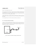
Page 86: ...Class D amplifier whose maximum output power is 1 5W when the load is 8Ω The headphone interface features stereo left and right channel output and headphone insertion detection function is supported 3 22 1 Reference Circuit Design for Microphone Interface MIC1_P ECM Type R2 R1 Module D1 MIC1_N 33pF 0R 0R R3 0R Figure 30 Reference Circuit Design for Analog ECM type Microphone EAR_P 53 AO Earpiece o...

Page 87: ...Module MIC_GND 0R MIC_BIAS 1 2 3 4 F1 D1 OUT GND GND VDD 100nF C4 0R D2 R3 0R Figure 31 Reference Circuit Design for MEMS type Microphone 3 22 2 Reference Circuit Design for Earpiece Interface EAR_P EAR_M 33pF 33pF 33pF C2 C3 C1 Module D1 D2 F1 F2 Figure 32 Reference Circuit Design for Earpiece Interface ...

Page 88: ...udspeaker Interface 3 22 5 Audio Interfaces Design Considerations It is recommended to use the electret microphone with dual built in capacitors e g 10pF and 33pF for filtering out RF interference thus reducing TDD noise The 33pF capacitor is applied for filtering out RF interference when the module is transmitting at EGSM900 Without placing this capacitor TDD noise could be heard The 10pF capacit...

Page 89: ...RF antennas should be placed away from audio interfaces and audio traces Power traces cannot be parallel with and also should be far away from the audio traces The differential audio traces must be routed according to the differential signal layout rule 3 23 Emergency Download Interface USB_BOOT is an emergency download interface Pulling up LDO13A_1P8 during power up will force the module into eme...

Page 90: ...i Fi Overview SC66 module supports 2 4GHz and 5GHz dual band WLAN wireless communication based on IEEE 802 11a b g n ac standard protocols The maximum data rate is up to 433Mbps The features are below Support Wake on WLAN WoWLAN Support ad hoc mode Support WAPI SMS4 hardware encryption Support AP mode Support Wi Fi Direct Support MCS 0 7 for HT20 and HT40 Support MCS 0 8 for VHT20 Support MCS 0 9 ...

Page 91: ...m 2 5dB 802 11n HT20 MCS0 15dBm 2 5dB 802 11n HT20 MCS7 13dBm 2 5dB 802 11n HT40 MCS0 15dBm 2 5dB 802 11n HT40 MCS7 13dBm 2 5dB 802 11ac VHT20 MCS0 14dBm 2 5dB 802 11ac VHT20 MCS8 13dBm 2 5dB 802 11ac VHT40 MCS0 13dBm 2 5dB 802 11ac VHT40 MCS9 12dBm 2 5dB 802 11ac VHT80 MCS0 13dBm 2 5dB 802 11ac VHT80 MCS9 12dBm 2 5dB Standard Rate Sensitivity 2 4GHz 802 11b 1Mbps 96dBm 802 11b 11Mbps 87dBm 802 11...

Page 92: ...low Control the impedance of either feeder line or PCB trace in Wi Fi MIMO part to 50Ω and keep the trace length as short as possible Maximize the distance between Wi Fi MIMO antenna and DSI trace including trace routing and antenna layout to avoid mutual interference Space for locating EMI filter should be reserved in DSI trace 4 2 BT Overview SC66 module supports BT5 0 BR EDR BLE specifications ...

Page 93: ...1 EDR 3 0 3 0 HS August 6 2009 Bluetooth Low Energy RF PHY Test Specification RF PHY TS 4 0 0 December 15 2009 Bluetooth 5 0 RF PHY Cover Standard RF PHY TS 5 0 0 December 06 2016 4 2 1 BT Performance The following table lists the BT transmitting and receiving performance of SC66 module Table 34 BT Transmitting and Receiving Performance Version Data rate Maximum Application Throughput Comment 1 2 ...

Page 94: ...NASS and BeiDou With an embedded LNA the module provides greatly improved positioning accuracy 5 1 GNSS Performance The following table lists the GNSS performance of SC66 module in conduction mode Table 35 GNSS Performance Parameter Description Typ Unit Sensitivity GNSS Cold start 144 dBm Reacquisition 157 dBm Tracking 157 dBm TTFF GNSS Cold start 32 s Warm start 30 s Hot start 5 s Static Drift GN...

Page 95: ...S RF signal lines and RF components should be placed far away from high speed circuits switched mode power supplies power inductors the clock circuit of single chip microcomputers etc For applications with harsh electromagnetic environment or high ESD protection requirements it is recommended to add ESD protective diodes for the antenna interface Only diodes with ultra low junction capacitance suc...

Page 96: ...tenna interfaces is shown below Table 36 Pin Definition of Main Rx diversity Antenna Interfaces The operating frequencies of SC66 module are listed in the following tables Table 37 SC66 CE Operating Frequencies Pin Name Pin No I O Description Comment ANT_MAIN 19 IO Main antenna interface 50Ω impedance ANT_DRX 149 AI Diversity antenna interface 50Ω impedance 3GPP Band Receive Transmit Unit EGSM900 ...

Page 97: ...2620 MHz LTE TDD B39 1880 1920 1880 1920 MHz LTE TDD B40 2300 2400 2300 2400 MHz LTE TDD B41 1 2555 2655 2555 2655 MHz 3GPP Band Receive Transmit Unit WCDMA B2 1930 1990 1850 1910 MHz WCDMA B4 2110 2155 1710 1755 MHz WCDMA B5 869 894 824 849 MHz LTE FDD B2 1930 1990 1850 1910 MHz LTE FDD B4 2110 2155 1710 1755 MHz LTE FDD B5 869 894 824 849 MHz LTE FDD B7 2620 2690 2500 2570 MHz LTE FDD B12 729 74...

Page 98: ...B1 2110 2170 1920 1980 MHz WCDMA B6 875 885 830 840 MHz WCDMA B8 925 960 880 915 MHz WCDMA B19 875 890 830 845 MHz LTE FDD B1 2110 2170 1920 1980 MHz LTE FDD B3 1805 1880 1710 1785 MHz LTE FDD B5 869 894 824 849 MHz LTE FDD B8 925 960 880 915 MHz LTE FDD B11 1476 1496 1428 1448 MHz LTE FDD B18 860 875 815 830 MHz LTE FDD B19 875 890 830 845 MHz LTE FDD B21 1496 1511 1448 1463 MHz LTE FDD B26 859 8...

Page 99: ...B4 2110 2155 1710 1755 MHz WCDMA B5 869 894 824 849 MHz WCDMA B8 925 960 880 915 MHz LTE FDD B1 2110 2170 1920 1980 MHz LTE FDD B2 1930 1990 1850 1910 MHz LTE FDD B3 1805 1880 1710 1785 MHz LTE FDD B4 2110 2155 1710 1755 MHz LTE FDD B5 869 894 824 849 MHz LTE FDD B7 2620 2690 2500 2570 MHz LTE FDD B8 925 960 880 915 MHz LTE FDD B20 791 821 832 862 MHz LTE FDD B28 A B 758 803 703 748 MHz LTE TDD B3...

Page 100: ...etter RF performance and the π type matching components R1 C1 C2 R2 C3 C4 should be placed as close to the antennas as possible The capacitors are not mounted by default and resistors are 0Ω ANT_MAIN R1 0R C1 Module Main antenna NM C2 NM R2 0R C3 Diversity antenna NM C4 NM ANT_DRX Figure 36 Reference Circuit Design for Main and Rx diversity Antenna Interfaces 6 1 2 Reference Design of RF Layout Fo...

Page 101: ...The following are reference designs of microstrip line or coplanar waveguide with different PCB structures Figure 37 Microstrip Design on a 2 layer PCB Figure 38 Coplanar Waveguide Design on a 2 layer PCB Figure 39 Coplanar Waveguide Design on a 4 layer PCB Layer 3 as Reference Ground ...

Page 102: ...e as short as possible and all the right angle traces should be changed to curved ones There should be clearance under the signal pin of the antenna connector or solder joint The reference ground of RF traces should be complete Meanwhile adding some ground vias around RF traces and the reference ground could help to improve RF performance The distance between the ground vias and RF traces should b...

Page 103: ...ter RF performance The capacitors are not mounted by default and resistors are 0Ω ANT_WIFI BT R1 0R C1 Module NM C2 NM Figure 41 Reference Circuit Design for Wi Fi BT Antenna Interface A reference circuit design for Wi Fi MIMO antenna interface is shown below A π type matching circuit is recommended to be reserved for better RF performance The capacitors are not mounted by default and resistors ar...

Page 104: ... 6 3 GNSS Antenna Interface Table 43 Pin Definition of GNSS Antenna Table 44 GNSS Frequency Pin Name Pin No I O Description Comment ANT_GNSS 134 AI GNSS antenna Interface 50Ω impedance GNSS_PPS_OUT 202 DO LNA enable control For test purpose only If unused keep it open Cannot be pulled up Type Frequency Unit GPS 1575 42 1 023 MHz GLONASS 1597 5 1605 8 MHz BeiDou 1561 098 2 046 MHz ...

Page 105: ...that is the antenna trace is long and the external loss is more than 2dB it is recommended to add an external LNA circuit for better GNSS receiving performance and the LNA should be placed close to the antenna 6 3 2 Recommended Circuit for Active Antenna The active antenna is powered by a 56nH inductor through the antenna s signal path The common power supply voltage ranges from 3 3V to 5 0V Altho...

Page 106: ...dule Series SC66 Hardware Design SC66_Hardware_Design 105 139 Active Antenna 3V3 Module ANT_GNSS 56nH 10R 1uF 100pF NM NM C4 C1 R1 L1 R2 0R C5 C3 C2 100pF Figure 44 Reference Circuit Design for GNSS Active Antenna ...

Page 107: ...Type Requirements GSM WCDMA TD SCDMA LTE VSWR 2 Gain dBi 1 Max Input Power W 50 Input Impedance Ω 50 Polarization Type Vertical Cable Insertion Loss 1dB frequency 663 960 MHz Cable Insertion Loss 1 5dB frequency 1427 2200 MHz Cable Insertion Loss 2dB frequency 2300 2690 MHz Wi Fi BT VSWR 2 Gain dBi 1 Max Input Power W 50 Input Impedance Ω 50 Polarization Type Vertical Cable Insertion Loss 1dB GNSS...

Page 108: ...stallation If RF connector is used for antenna connection it is recommended to use the U FL R SMT connector provided by HIROSE Figure 45 Dimensions of the U FL R SMT Connector Unit mm U FL LP serial connectors listed in the following figure can be used to match the U FL R SMT Figure 46 Mechanicals of U FL LP Connectors ...

Page 109: ...ries SC66 Hardware Design SC66_Hardware_Design 108 139 The following figure describes the space factor of mated connector Figure 47 Space Factor of Mated Connector Unit mm For more details please visit http www hirose com ...

Page 110: ...he following table Table 46 Absolute Maximum Ratings 7 2 Power Supply Ratings Table 47 SC66 Module Power Supply Ratings Parameter Min Max Unit VBAT 0 5 6 V USB_VBUS 0 5 16 V Current on VBAT 0 3 A Voltage on Digital Pins 0 3 2 093 V Parameter Description Conditions Min Typ Max Unit VBAT VBAT The actual input voltages must stay between the minimum and maximum values 3 55 4 0 4 4 V Voltage drop durin...

Page 111: ...s no unrecoverable malfunction There are also no effects on radio spectrum and no harm to radio network Only one or more parameters like Pout might reduce in their value and exceed the specified tolerances When the temperature returns to the normal operating temperature levels the module will meet 3GPP specifications again IVBAT Peak supply current during transmission slot Maximum power control le...

Page 112: ... TBD TBD TBD mA Sleep USB disconnected DRX 8 TBD TBD TBD mA Sleep USB disconnected DRX 9 TBD TBD TBD mA CDMA supply current BC0 CH283 Slot Cycle Index 1 TBD TBD TBD mA BC0 CH283 Slot Cycle Index 7 TBD TBD TBD mA TD SCDMA supply current Sleep USB disconnected DRX 6 TBD TBD TBD mA Sleep USB disconnected DRX 8 TBD TBD TBD mA Sleep USB disconnected DRX 9 TBD TBD TBD mA LTE FDD supply current Sleep USB...

Page 113: ...M900 1UL 4DL PCL 5 TBD TBD TBD mA EGSM900 2UL 3DL PCL 5 TBD TBD TBD mA EGSM900 3UL 2DL PCL 5 TBD TBD TBD mA EGSM900 4UL 1DL PCL 5 TBD TBD TBD mA DCS1800 1UL 4DL PCL 0 TBD TBD TBD mA DCS1800 2UL 3DL PCL 0 TBD TBD TBD mA DCS1800 3UL 2DL PCL 0 TBD TBD TBD mA DCS1800 4UL 1DL PCL 0 TBD TBD TBD mA EDGE data transfer EGSM900 1UL 4DL PCL 8 TBD TBD TBD mA EGSM900 2UL 3DL PCL 8 TBD TBD TBD mA EGSM900 3UL 2D...

Page 114: ...TE FDD B1 max power TBD TBD TBD mA LTE FDD B3 max power TBD TBD TBD mA LTE FDD B5 max power TBD TBD TBD mA LTE FDD B8 max power TBD TBD TBD mA LTE TDD B34 max power TBD TBD TBD mA LTE TDD B38 max power TBD TBD TBD mA LTE TDD B39 max power TBD TBD TBD mA LTE TDD B40 max power TBD TBD TBD mA LTE TDD B41 max power TBD TBD TBD mA Parameter Description Conditions Min Typ Max Unit IVABT Power down OFF s...

Page 115: ...BD mA WCDMA data transfer B2 HSDPA max power TBD TBD TBD mA B4 HSDPA max power TBD TBD TBD mA B5 HSDPA max power TBD TBD TBD mA B2 HSUPA max power TBD TBD TBD mA B4 HSUPA max power TBD TBD TBD mA B5 HSUPA max power TBD TBD TBD mA LTE data transfer LTE FDD B2 max power TBD TBD TBD mA LTE FDD B4 max power TBD TBD TBD mA LTE FDD B5 max power TBD TBD TBD mA LTE FDD B7 max power TBD TBD TBD mA LTE TDD ...

Page 116: ...D TBD mA Sleep USB disconnected DRX 9 TBD TBD TBD mA LTE FDD supply current Sleep USB disconnected DRX 6 TBD TBD TBD mA Sleep USB disconnected DRX 8 TBD TBD TBD mA Sleep USB disconnected DRX 9 TBD TBD TBD mA LTE TDD supply current Sleep USB disconnected DRX 6 TBD TBD TBD mA Sleep USB disconnected DRX 8 TBD TBD TBD mA Sleep USB disconnected DRX 9 TBD TBD TBD mA WCDMA voice call B1 max power TBD TBD...

Page 117: ...TE FDD B8 max power TBD TBD TBD mA LTE FDD B11 max power TBD TBD TBD mA LTE FDD B18 max power TBD TBD TBD mA LTE FDD B19 max power TBD TBD TBD mA LTE FDD B21 max power TBD TBD TBD mA LTE FDD B26 max power TBD TBD TBD mA LTE FDD B28 A B max power TBD TBD TBD mA LTE TDD B41 max power TBD TBD TBD mA Parameter Description Conditions Min Typ Max Unit IVBAT Power down OFF state TBD TBD TBD uA GSM GPRS s...

Page 118: ...A Sleep USB disconnected DRX 8 TBD TBD TBD mA Sleep USB disconnected DRX 9 TBD TBD TBD mA GSM voice call GSM850 PCL 5 TBD TBD TBD mA GSM850 PCL 12 TBD TBD TBD mA GSM850 PCL 19 TBD TBD TBD mA EGSM900 PCL 5 TBD TBD TBD mA EGSM900 PCL 12 TBD TBD TBD mA EGSM900 PCL 19 TBD TBD TBD mA DCS1800 PCL 0 TBD TBD TBD mA DCS1800 PCL 7 TBD TBD TBD mA DCS1800 PCL 15 TBD TBD TBD mA PCS1900 PCL 0 TBD TBD TBD mA PCS...

Page 119: ...D mA DCS1800 1UL 4DL PCL 0 TBD TBD TBD mA DCS1800 2UL 3DL PCL 0 TBD TBD TBD mA DCS1800 3UL 2DL PCL 0 TBD TBD TBD mA DCS1800 4UL 1DL PCL 0 TBD TBD TBD mA PCS1900 1UL 4DL PCL 0 TBD TBD TBD mA PCS1900 2UL 3DL PCL 0 TBD TBD TBD mA PCS1900 3UL 2DL PCL 0 TBD TBD TBD mA PCS1900 4UL 1DL PCL 0 TBD TBD TBD mA EDGE data transfer GSM850 1UL 4DL PCL 8 TBD TBD TBD mA GSM850 2UL 3DL PCL 8 TBD TBD TBD mA GSM850 3...

Page 120: ...max power TBD TBD TBD mA B2 HSDPA max power TBD TBD TBD mA B4 HSDPA max power TBD TBD TBD mA B5 HSDPA max power TBD TBD TBD mA B8 HSDPA max power TBD TBD TBD mA B1 HSUPA max power TBD TBD TBD mA B2 HSUPA max power TBD TBD TBD mA B4 HSUPA max power TBD TBD TBD mA B5 HSUPA max power TBD TBD TBD mA B8 HSUPA max power TBD TBD TBD mA LTE data transfer LTE FDD B1 max power TBD TBD TBD mA LTE FDD B2 max ...

Page 121: ...BD mA LTE FDD B28 A B max power TBD TBD TBD mA LTE TDD B41 max power TBD TBD TBD mA Frequency Max Min EGSM900 33dBm 2dB 5dBm 5dB DCS1800 30dBm 2dB 0dBm 5dB WCDMA B1 24dBm 1 3dB 49dBm WCDMA B8 24dBm 1 3dB 49dBm EVDO CDMA BC0 24dBm 3 1dB 49dBm TD SCDMA B34 24dBm 1 3dB 49dBm TD SCDMA B39 24dBm 1 3dB 49dBm LTE FDD B1 23dBm 2dB 39dBm LTE FDD B3 23dBm 2dB 39dBm LTE FDD B5 23dBm 2dB 39dBm LTE FDD B8 23dB...

Page 122: ...CDMA B2 24dBm 1 3dB 49dBm WCDMA B4 24dBm 1 3dB 49dBm WCDMA B5 24dBm 1 3dB 49dBm LTE FDD B2 23dBm 2dB 39dBm LTE FDD B4 23dBm 2dB 39dBm LTE FDD B5 23dBm 2dB 39dBm LTE FDD B7 23dBm 2dB 39dBm LTE FDD B12 23dBm 2dB 39dBm LTE FDD B13 23dBm 2dB 39dBm LTE FDD B14 23dBm 2dB 39dBm LTE FDD B17 23dBm 2dB 39dBm LTE FDD B25 23dBm 2dB 39dBm LTE FDD B26 23dBm 2dB 39dBm LTE FDD B66 23dBm 2dB 39dBm LTE TDD B71 23dB...

Page 123: ...dBm LTE FDD B1 23dBm 2dB 39dBm LTE FDD B3 23dBm 2dB 39dBm LTE FDD B5 23dBm 2dB 39dBm LTE FDD B8 23dBm 2dB 39dBm LTE FDD B11 23dBm 2dB 39dBm LTE FDD B18 23dBm 2dB 39dBm LTE FDD B19 23dBm 2dB 39dBm LTE FDD B21 23dBm 2dB 39dBm LTE FDD B26 23dBm 2dB 39dBm LTE FDD B28 A B 23dBm 2dB 39dBm LTE TDD B41 23dBm 2dB 39dBm Frequency Max Min GSM850 33dBm 2dB 5dBm 5dB EGSM900 33dBm 2dB 5dBm 5dB DCS1800 30dBm 2dB...

Page 124: ...A B2 24dBm 1 3dB 49dBm WCDMA B4 24dBm 1 3dB 49dBm WCDMA B5 24dBm 1 3dB 49dBm WCDMA B8 24dBm 1 3dB 49dBm LTE FDD B1 23dBm 2dB 39dBm LTE FDD B2 23dBm 2dB 39dBm LTE FDD B3 23dBm 2dB 39dBm LTE FDD B4 23dBm 2dB 39dBm LTE FDD B5 23dBm 2dB 39dBm LTE FDD B7 23dBm 2dB 39dBm LTE FDD B8 23dBm 2dB 39dBm LTE FDD B20 23dBm 2dB 39dBm LTE FDD B28 A B 23dBm 2dB 39dBm LTE TDD B38 23dBm 2dB 39dBm LTE TDD B39 23dBm 2...

Page 125: ...m WCDMA B1 110dBm 106 7dBm WCDMA B8 110dBm 103 7dBm EVDO CDMA BC0 109dBm 104dBm TD SCDMA B34 109dBm 108dBm TD SCDMA B39 109dBm 108dBm LTE FDD B1 10M 98dBm 98 5dBm 101 2dBm 96 3dBm LTE FDD B3 10M 98dBm 98 5dBm 101 2dBm 93 3dBm LTE FDD B5 10M 98dBm 99dBm 101 5dBm 94 3dBm LTE FDD B8 10M 98dBm 99dBm 101 5dBm 93 3dBm LTE TDD B34 10M 98dBm 98dBm 101dBm 96 3dBm LTE TDD B38 10M 97 5dBm 98dBm 100 5dBm 96 3...

Page 126: ...DMA B5 104 7dBm LTE FDD B2 10M 94 3dBm LTE FDD B4 10M 96 3dBm LTE FDD B5 10M 94 3dBm LTE FDD B7 10M 94 3dBm LTE FDD B12 10M 93 3dBm LTE FDD B13 10M 93 3dBm LTE FDD B14 10M 93 3dBm LTE FDD B17 10M 93 3dBm LTE FDD B25 10M 92 8dBm LTE FDD B66 10M 95 8dBm LTE TDD B71 10M 93 5dBm LTE TDD B41 10M 94 3dBm Frequency Receive Sensitivity Typ 3GPP SIMO Primary Diversity SIMO WCDMA B1 106 7dBm WCDMA B6 106 7d...

Page 127: ...FDD B18 10M 96 3dBm LTE FDD B19 10M 96 3dBm LTE FDD B21 10M 96 3dBm LTE FDD B26 10M 93 8dBm LTE FDD B28 A B 10M 94 8dBm LTE TDD B41 10M 94 3dBm Frequency Receive Sensitivity Typ 3GPP SIMO Primary Diversity SIMO GSM850 102 4dBm EGSM900 102 4dBm DCS1800 102 4dBm PCS1900 102 4dBm WCDMA B1 106 7dBm WCDMA B2 104 7dBm WCDMA B4 106 7dBm WCDMA B5 104 7dBm WCDMA B8 103 7dBm LTE FDD B1 10M 96 3dBm LTE FDD B...

Page 128: ...der development LTE FDD B3 10M 93 3dBm LTE FDD B4 10M 96 3dBm LTE FDD B5 10M 94 3dBm LTE FDD B7 10M 94 3dBm LTE FDD B8 10M 93 3dBm LTE FDD B20 10M 93 3dBm LTE FDD B28 A B 10M 94 8dBm LTE TDD B38 10M 96 3dBm LTE TDD B39 10M 96 3dBm LTE TDD B40 10M 96 3dBm LTE TDD B41 10M 94 3dBm NOTE ...

Page 129: ...applied to ESD sensitive components Proper ESD handling and packaging procedures must be applied throughout the processing handling and operation of any application that incorporates the module The following table shows the electrostatic discharge characteristics of SC66 module Table 61 ESD Characteristics Temperature 25 C Humidity 45 Test Points Contact Discharge Air Discharge Unit VBAT GND 5 10 ...

Page 130: ...al Dimensions This chapter describes the mechanical dimensions of the module All dimensions are measured in millimeter mm and the dimensional tolerances are 0 05mm unless otherwise specified 8 1 Mechanical Dimensions of the Module Top view Pin1 Figure 48 Module Top and Side Dimensions ...

Page 131: ...Smart LTE Module Series SC66 Hardware Design SC66_Hardware_Design 130 139 Figure 49 Module Bottom Dimensions Top View ...

Page 132: ...ign 131 139 8 2 Recommended Footprint Figure 50 Recommended Footprint Top View 1 For easy maintenance of the module keep about 3mm between the module and other components on host PCB 2 All RESERVED pins should be kept open and MUST NOT be connected to ground NOTES ...

Page 133: ..._Design 132 139 8 3 Top and Bottom View of the Module Figure 51 Top View of the Module Figure 52 Bottom View of the Module These are renderings of SC66 module For authentic dimension and appearance please refer to the module that you receive from Quectel NOTE ...

Page 134: ... at the factory environment of 30ºC 60 RH Stored at 10 RH 3 Devices require baking before mounting if any circumstance below occurs When the ambient temperature is 23ºC 5ºC and the humidity indication card shows the humidity is 10 before opening the vacuum sealed bag Device mounting cannot be finished within 168 hours at factory conditions of 30ºC 60 4 If baking is required devices may be baked fo...

Page 135: ... details please refer to document 4 It is suggested that the peak reflow temperature is 238 245ºC and the absolute maximum reflow temperature is 245ºC To avoid damage to the module caused by repeated heating it is strongly recommended that the module should be mounted after reflow soldering for the other side of PCB has been completed The recommended reflow soldering thermal profile lead free refl...

Page 136: ...el carriers Each reel is 330mm in diameter and contains 200 modules The following figures show the package details measured in mm Figure 54 Tape Dimensions Reflow Zone Max slope 2 to 3 C sec Reflow time D over 220 C 40 to 60 sec Max temperature 238 C 245 C Cooling down slope 1 to 4 C sec Reflow Cycle Max reflow cycle 1 ...

Page 137: ...SC66_Hardware_Design 136 139 Figure 55 Reel Dimensions Table 63 Reel Packaging Model Name MOQ for MP Minimum Package 200pcs Minimum Package 4 800pcs SC66 200 Size 398mm 383mm 83mm N W 1 92kg G W 3 67kg Size 420mm 350mm 405mm N W 8 18kg G W 15 18kg ...

Page 138: ...CSD Circuit Switched Data CTS Clear to Send DP DisplayPort DRX Discontinuous Reception EFR Enhanced Full Rate EGSM Extended GSM900 band includes standard GSM900 band SN Document Name Remark 1 Quectel_Smart_EVB G2_User_Guide EVB User Guide for SC66 2 Quectel_SC66_GPIO_Configuration GPIO Configuration of SC66 3 Quectel_RF_Layout_Application_Note RF Layout Application Note 4 Quectel_Module_Secondary_...

Page 139: ...Rate HSDPA High Speed Down Link Packet Access HSPA High Speed Packet Access I O Input Output IQ Inphase and Quadrature LCD Liquid Crystal Display LCM LCD Module LED Light Emitting Diode LNA Low Noise Amplifier LRA Linear Resonant Actuator LTE TDD Long Term Evolution Time Division Duplex MIPI Mobile Industry Processor Interface PCB Printed Circuit Board PDU Protocol Data Unit PMI Power Management I...

Page 140: ...n UART Universal Asynchronous Receiver Transmitter UMTS Universal Mobile Telecommunications System U SIM Universal Subscriber Identity Module Vmax Maximum Voltage Value Vnorm Normal Voltage Value Vmin Minimum Voltage Value VI Voltage Input VIHmin Minimum Input High Level Voltage Value VILmax Maximum Input Low Level Voltage Value VO Voltage Output VOHmin Minimum Output High Level Voltage Value VOLm...

Page 141: ...Schemes Table 66 Description of Different Coding Schemes Scheme CS 1 CS 2 CS 3 CS 4 Code Rate 1 2 2 3 3 4 1 USF 3 3 3 3 Pre coded USF 3 6 6 12 Radio Block excl USF and BCS 181 268 312 428 BCS 40 16 16 16 Tail 4 4 4 Coded Bits 456 588 676 456 Punctured Bits 0 132 220 Data Rate Kb s 9 05 13 4 15 6 21 4 ...

Page 142: ...or 2 2 the first number indicates the amount of downlink timeslots while the second number indicates the amount of uplink timeslots The active slots determine the total number of slots the GPRS device can use simultaneously for both uplink and downlink communications The description of different multi slot classes is shown in the following table Table 67 GPRS Multi slot Classes Multislot Class Dow...

Page 143: ...are Design SC66_Hardware_Design 142 139 14 4 4 NA 15 5 5 NA 16 6 6 NA 17 7 7 NA 18 8 8 NA 19 6 2 NA 20 6 3 NA 21 6 4 NA 22 6 4 NA 23 6 6 NA 24 8 2 NA 25 8 3 NA 26 8 4 NA 27 8 4 NA 28 8 6 NA 29 8 8 NA 30 5 1 6 31 5 2 6 32 5 3 6 33 5 4 6 ...

Page 144: ... 2 GMSK 13 4kbps 26 8kbps 53 6kbps CS 3 GMSK 15 6kbps 31 2kbps 62 4kbps CS 4 GMSK 21 4kbps 42 8kbps 85 6kbps MCS 1 GMSK C 8 80kbps 17 60kbps 35 20kbps MCS 2 GMSK B 11 2kbps 22 4kbps 44 8kbps MCS 3 GMSK A 14 8kbps 29 6kbps 59 2kbps MCS 4 GMSK C 17 6kbps 35 2kbps 70 4kbps MCS 5 8 PSK B 22 4kbps 44 8kbps 89 6kbps MCS 6 8 PSK A 29 6kbps 59 2kbps 118 4kbps MCS 7 8 PSK B 44 8kbps 89 6kbps 179 2kbps MCS ...

Page 145: ... and cable loss must satisfy MPE categorical Exclusion Requirements of 2 1091 2 The EUT is a mobile device maintain at least a 20 cm separation between the EUT and the user s body and must not transmit simultaneously with any other antenna or transmitter 3 A label with the following statements must be attached to the host end product This device contains FCC ID XMR2019SC66A 4 To comply with FCC re...

Page 146: ...ts of FCC Part 2 1093 If the device is used for other equipment that separate approval is required for all other operating configurations including portable configurations with respect to 2 1093 and different antenna configurations For this device OEM integrators must be provided with labeling instructions of finished products Please refer to KDB784748 D01 v07 section 8 Page 6 7 last two paragraph...

Page 147: ... the manufacturer could void the user s authority to operate the equipment To ensure compliance with all non transmitter functions the host manufacturer is responsible for ensuring compliance with the module s installed and fully operational For example if a host was previously authorized as an unintentional radiator under the Supplier s Declaration of Conformity procedure without a transmitter ce...

Page 148: ...eceded by the word Contains or similar wording expressing the same meaning as follows Contains IC 10224A 2019SC66A or where 10224A 2019SC66A is the module s certification number Le produit hôte doit être correctement étiqueté pour identifier les modules dans le produit hôte L étiquette de certification d Innovation Sciences et Développement économique Canada d un module doit être clairement visibl...

Reviews: