Smart LTE Module Series
SC66 Hardware Design
SC66_Hardware_Design 75 / 139
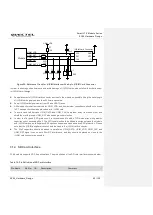
TP0_RST
TP0_I2C_SCL
TP0_I2C_SDA
TP0_INT
1
2
3
4
5
6
2.2K
2.2K
4.7uF 100nF
Module
RESET 1.8V
SCL 1.8V
SDA 1.8V
INT 1.8V
GND
VDD 2.8V
TP
R2
R1
C1
C2
D1
D2
D3
D4
D5
LDO3B_2P8
LDO11A_1P8
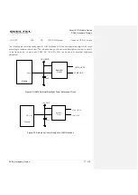
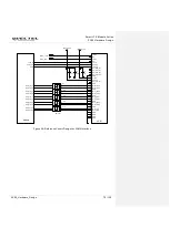
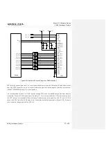
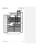
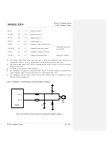
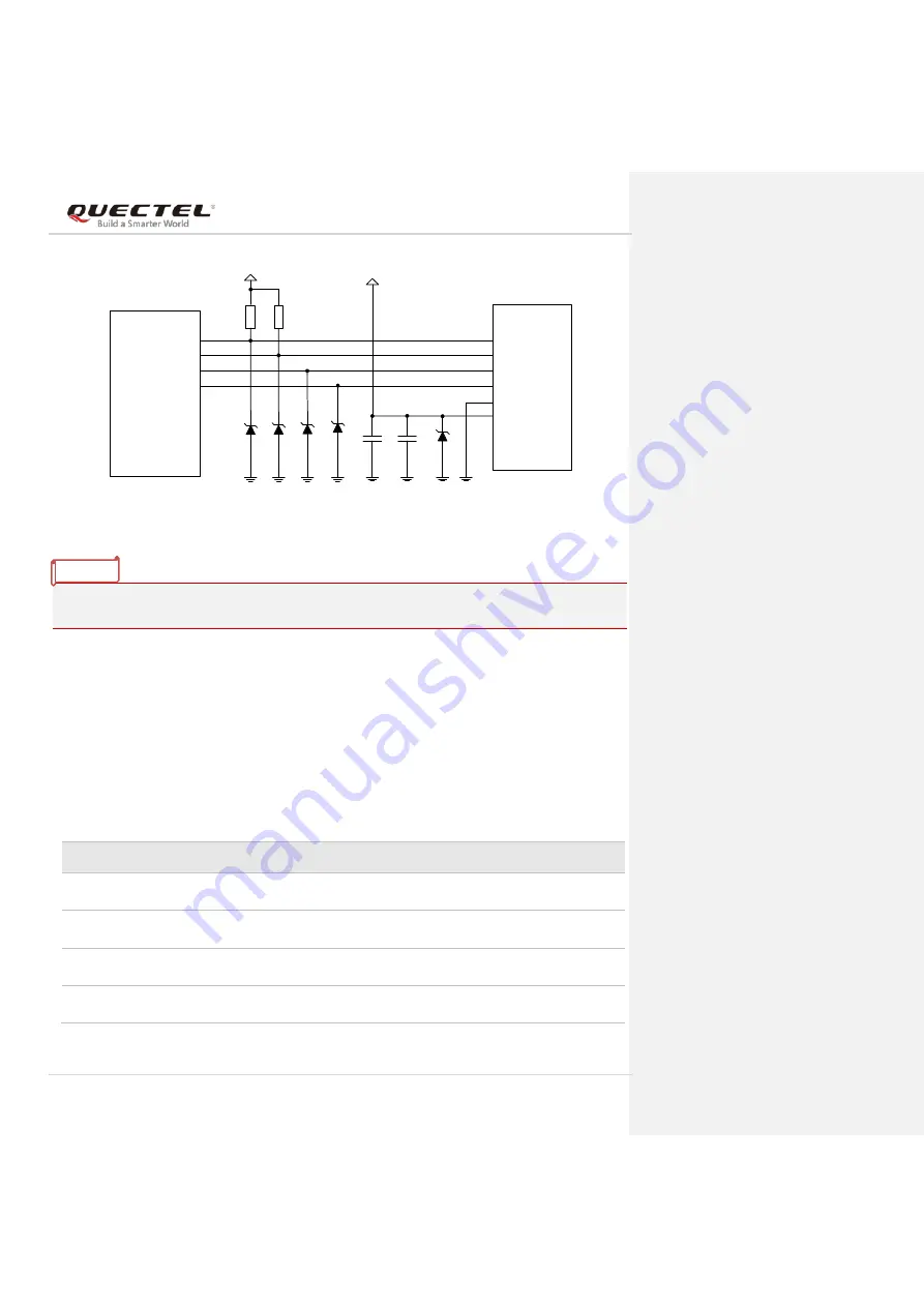
Figure 26: Reference Circuit Design for TP0 Interface
The reference circuit design of TP1 is similar to that of TP0. Please refer to TP0 reference circuit design
for TP1.
3.20. Camera Interfaces
Based on standard MIPI CSI input interface, SC66 module supports 3 cameras (4-lane + 4-lane + 4-lane)
or 4 cameras (4-lane + 4-lane + 2-lane + 1-lane), with maximum pixels up to 24MP for SC66. The video
and photo quality are determined by various factors such as camera sensor, camera lens quality, etc.
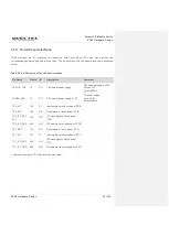
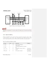
Table 27: Pin Definition of Camera Interfaces
Pin Name
Pin No.
I/O
Description
Comment
GPIO_08B
13
DO
Rear camera DVDD power
LDO enable pin
GPIO_05B
15
IO
Front camera DVDD power LDO enable
pin
LDO11A_1P8
10
PO
1.8V output power supply Power for
DOVDD
Vnorm=1.8V
I
O
max=150mA
LDO3B_2P8
12
PO
2.8V output power supply
Vnorm=2.8V
I
O
max=600mA
NOTE

