background image


UMTS/HSPA  Module  Series 

                                                                                                                                UC20  Hardware  Design


UC20_Hardware_Design                                Confidential / Released                                                53 / 84 


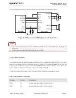
VDD_MCU

10K

Module

STATUS

MCU_GPIO

Module

STATUS

VBAT

2.2K


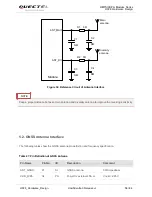
Figure 32: Reference Circuit of the STATUS 


3.16.2.  SLEEP_IND 

The SLEEP_IND is an indicated pin for judging whether the module is in sleep mode or not. When the 
module enters into the sleep mode, the SLEEP_IND will output a logic high level. So  you can use the 
SLEEP_IND for low current indication. The following table shows the pin definition of SLEEP_IND. 
 

Table 22: Pin Definition of SLEEP_IND 

Pin Name   

Pin No. 

I/O 

Description   

Comment 

SLEEP_IND 

DO 

Indicate the sleep status.   

1.8V power domain. 
Outputs high level when the 
module is in sleep mode. 


Summary of Contents for UC20

Page 1: ...UC20 Hardware Design UMTS HSPA Module Series Rev UC20_Hardware_Design_V1 2 Date 2014 01 13 www quectel com...

Page 2: ...OVIDED IS BASED UPON CUSTOMERS REQUIREMENTS QUECTEL MAKES EVERY EFFORT TO ENSURE THE QUALITY OF THE INFORMATION IT MAKES AVAILABLE QUECTEL DOES NOT MAKE ANY WARRANTY AS TO THE INFORMATION CONTAINED HE...

Page 3: ...HOU 1 Added UC20 G information 2 Added AMR WB feature 3 Added USB upgrade test points diagram 4 Added reference design of transistor circuit on UART interface 5 Deleted debug function of Debug UART in...

Page 4: ...2 Pin Assignment 18 3 3 Pin Description 19 3 4 Operating Modes 25 3 5 Power Saving 25 3 5 1 Sleep Mode 25 3 5 1 1 UART Application 26 3 5 1 2 USB Application with Suspend Function 26 3 5 1 3 USB Appl...

Page 5: ...58 5 1 1 Pin Definition 58 5 1 2 Operating Frequency 58 5 1 3 Reference Design 58 5 2 GNSS Antenna Interface 59 5 2 1 Reference Design for Passive Antenna 60 5 2 2 Reference Design for Active Antenna...

Page 6: ...UMTS HSPA Module Series UC20 Hardware Design UC20_Hardware_Design Confidential Released 5 84 8 2 Manufacturing and Welding 74 8 3 Packaging 75 9 Appendix A Reference 77...

Page 7: ...16 PIN DEFINITION OF PCM AND I2C INTERFACE 49 TABLE 17 PIN DEFINITION OF THE ADC 50 TABLE 18 CHARACTERISTIC OF THE ADC 51 TABLE 19 PIN DEFINITION OF NETWORK INDICATOR 51 TABLE 20 WORKING STATE OF THE...

Page 8: ...RE 19 REFERENCE CIRCUIT WITH TRANSISTOR CIRCUIT 40 FIGURE 20 RS232 LEVEL MATCH CIRCUIT 41 FIGURE 21 REFERENCE CIRCUIT OF DEBUG UART WITH LEVEL TRANSLATOR 41 FIGURE 22 REFERENCE CIRCUIT OF THE 8 PIN US...

Page 9: ...Design Confidential Released 8 84 FIGURE 42 BOTTOM PADS DIMENSIONS BOTTOM VIEW 71 FIGURE 43 RECOMMENDED FOOTPRINT TOP VIEW 72 FIGURE 44 TOP VIEW OF THE MODULE 73 FIGURE 45 BOTTOM VIEW OF THE MODULE 73...

Page 10: ...odule and describes its hardware interface which are connected with your application and the air interface This document can help you quickly understand module interface specifications electrical and...

Page 11: ...s devices on boarding the aircraft if your device offers a Airplane Mode which must be enabled prior to boarding an aircraft Switch off your wireless device when in hospitals or clinics or other healt...

Page 12: ...ts for M2M application such as automotive metering tracking system security solutions routers wireless POS mobile computing devices PDA phone and tablet PC etc UC20 is an SMD type module which can be...

Page 13: ...talled and operated with minimum distance 20cm between the radiator and your body as well as kept minimum 20cm from radio antenna depending on the Mobile status of this module usage This module should...

Page 14: ...t both 16 QAM and QPSK modulation Internet Protocol Features Support TCP PPP UDP protocols Support the protocols PAP Password Authentication Protocol and CHAP Challenge Handshake Authentication Protoc...

Page 15: ...tion data transmission GNSS NMEA output software debug and firmware upgrade USB Driver Windows XP Windows Vista Windows 7 Windows 8 Windows CE5 0 6 0 Linux 2 6 3 0 Android 2 3 4 0 Rx diversity Support...

Page 16: ...ctional Diagram The following figure shows a block diagram of UC20 and illustrates the major functional parts Power management Baseband DDR NAND flash Radio frequency Peripheral interface UART interfa...

Page 17: ...US ADC PCM UART VBAT_BB USB ANT_DIV VBAT_RF VDD_EXT GSM UMTS RF Switch VDD_2V85 WAKEUP_IN VRTC SLEEP_IND W_DISABLE NAND Flash Figure 1 Functional Diagram 2 5 Evaluation Board In order to help you to d...

Page 18: ...ption UC20 is equipped with a 72 pin 1 3mm pitch SMT pads plus 40 pin ground pads and reserved pads that connect to cellular application platform Sub interfaces included in these pads are described in...

Page 19: ...ND RESET_N PWRKEY AGND RESERVED PCM_IN PCM_OUT PCM_SYNC PCM_CLK RESERVED RESERVED RESERVED RESERVED RESERVED RESERVED VDD_2V85 ANT_DIV GND GND USB_VBUS USB_DM USB_DP RXD TXD DTR RTS CTS DCD RI STATUS...

Page 20: ...drain Table 4 Pin Description Power Supply Pin Name Pin No I O Description DC Characteristics Comment VBAT_BB 59 60 PI Power supply for module baseband part Vmax 4 3V Vmin 3 4V Vnorm 3 8V It must be...

Page 21: ...RPU 200k VIHmax 2 1V VIHmin 1 3V VILmax 500mV Pull up to 1 8V internally RESET_N 20 DI Reset the module RPU 200k VIHmax 2 1V VIHmin 1 3V VILmax 500mV Pull up to 1 8V internally Active low Status Indi...

Page 22: ...I O Description DC Characteristics Comment USIM_GND 10 Specified ground for USIM card USIM_VDD 14 PO Power supply for USIM card For 1 8V USIM Vmax 1 98V Vmin 1 62V For 3 0V USIM Vmax 3 3V Vmin 2 7V IO...

Page 23: ...range 0 2V to 2 1V ADC1 44 AI General purpose analog to digital converter Voltage range 0 2V to 4 2V Main UART Interface Pin Name Pin No I O Description DC Characteristics Comment RI 62 DO Ring indica...

Page 24: ...pedance ANT_MAIN 49 IO Main antenna 50 impedance ANT_GNSS 47 AI GNNS antenna 50 impedance PCM Interface Pin Name Pin No I O Description DC Characteristics Comment PCM_IN 24 DI PCM data input VILmin 0...

Page 25: ...cription DC Characteristics Comment WAKEUP_ IN 1 DI Sleep mode control VILmin 0 3V VILmax 0 6V VIHmin 1 2V VIHmax 2 0V 1 8V power domain Pull up by default Low level wakes up the module W_DISABL E 4 D...

Page 26: ...and data transfer rate Minimum Functionality Mode AT CFUN command can set the module entering into a minimum functionality mode without removing the power supply In this case both RF function and USIM...

Page 27: ...e is used to wake up the processor and AP_READY will detect the sleep state of processor can be configured to high level or low level detection You should pay attention to the level match shown in dot...

Page 28: ...ume state the module will be woken up 3 5 1 3 USB Application without Suspend Function If application processor communicates with module via USB interface and processor does not support USB suspend fu...

Page 29: ...mode the RF function does not work and all AT commands correlative with RF function will be not accessible This mode can be set with the following way Hardware The W_DISABLE pin is pulled up by defaul...

Page 30: ...t 3 4 3 8 4 3 V GND 8 9 19 36 46 48 50 54 56 72 85 112 Ground 0 V 3 6 2 Decrease Voltage Drop The power supply range of the module is 3 4V 4 3V Because of the voltage drop during the transmitting time...

Page 31: ...2mm and the principle of the VBAT trace is the longer the wider 3 6 3 Reference Design for Power Supply The power design for the module is very important since the performance of power supply for the...

Page 32: ...down mode it can be turned on to normal mode by driving the PWRKEY pin to a low level at least 100ms It is recommended to use an open drain collector driver to control the PWRKEY You can monitor the...

Page 33: ...dule Series UC20 Hardware Design UC20_Hardware_Design Confidential Released 32 84 PWRKEY S1 Close to S1 TVS Figure 9 Turn on the Module Using Keystroke The turn on scenarios is illustrated as the foll...

Page 34: ...Turn off Module The following procedures can be used to turn off the module Normal power down procedure Turn off the module using the PWRKEY pin Normal power down procedure Turn off the module using c...

Page 35: ...ta loss If logging off is not done within 60s module will shut down internal power supply forcibly After that moment the module enters the power down mode no other AT commands can be executed and only...

Page 36: ...ised by command AT QCFG vbatt refer to document 1 for details 3 8 Reset the Module The RESET_N can be used to reset the module Table 8 RESET_N Pin Description Pin Name Pin No Description DC Characteri...

Page 37: ...0ms Figure 12 Reference Circuit of RESET_N by Using Driving Circuit RESET_N S2 Close to S2 TVS Figure 13 Reference Circuit of RESET_N by Using Button The reset scenario is illustrated as the following...

Page 38: ...is powered down and there is no power supply for the VBAT It is also available to charge the battery on the VRTC when module is turned on You can choose rechargeable battery capacitor or non recharge...

Page 39: ...e used for data transmission AT communication or firmware upgrade Debug UART interface supports 115200bps It can be used for GNSS NMEA sentences output USB interface supports software debug and firmwa...

Page 40: ...D 12 DO Transmit data 1 8V power domain DBG_RXD 11 DI Receive data 1 8V power domain The logic levels are described in the following table Table 11 Logic Levels of Digital I O Parameter Min Max Unit V...

Page 41: ...efer to the construction of solid line Please pay attention to direction of connection Input dotted line of module should refer to input solid line of the module Output dotted line of module should re...

Page 42: ...rovided by Texas Instruments is recommended VCCA VCCB OE A1 A2 GND B1 B2 VDD_EXT DBG_TXD DBG_RXD 0 1uF 0 1uF DBG_TXD_3 3V DBG_RXD_3 3V VDD_3 3V TXB0102DCU Figure 21 Reference Circuit of Debug UART wit...

Page 43: ...upported by the module automatically USIM_DATA 15 IO Data signal of USIM card Pull up to USIM_VDD with 15k resistor internally USIM_CLK 16 DO Clock signal of USIM card USIM_RST 17 DO Reset signal of U...

Page 44: ...iterion in the USIM circuit design Keep layout of USIM card as close as possible to the module Assure the length of the trace is less than 200mm Keep USIM card signal away from RF and VBAT alignment A...

Page 45: ...228 Please visit http www molex com for more information Figure 24 Molex 91228 USIM Connector Table 13 Pin Description of Molex USIM Connector Name Pin Function VDD C1 USIM card power supply RST C2 US...

Page 46: ...phenol C707 10M006 512 2 Please visit http www amphenol com for more information Figure 25 Amphenol C707 10M006 512 2 USIM Card Connector Table 14 Pin Description of Amphenol USIM Connector Name Pin F...

Page 47: ...of USB interface Table 15 USB Pin Description Pin Name Pin No I O Description Comment USB_DP 69 IO USB differential data bus positive Require differential impedance of 90 USB_DM 70 IO USB differentia...

Page 48: ...ay attention to the influence of junction capacitance of ESD component on USB data lines Typically the capacitance value should be less than 2pF e g ESD9L5 0ST5G Keep the ESD components as closer to t...

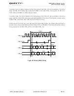
Page 49: ...n the falling edge of the PCM_CLK and transmitted on the rising edge while the PCM_SYNC rising edge represents the MSB In this mode PCM interface operates with a 128kHz PCM_CLK and an 8kHz 50 duty cyc...

Page 50: ...V power domain PCM_OUT 25 DO PCM data output 1 8V power domain PCM_SYNC 26 IO PCM data frame sync signal 1 8V power domain PCM_CLK 27 IO PCM data bit clock 1 8V power domain I2C_SCL 41 DO I2C serial c...

Page 51: ...2 UC20 work as a master device pertaining to I2C interface 3 14 ADC Function The module provides two analog to digital converters ADC to digitize the analog signal to 15 bit digital data such as batte...

Page 52: ...ODE and NET_STATUS The following tables describe pin definition and logic level changes in different network status Table 19 Pin Definition of Network Indicator Pin Name Pin No I O Description Comment...

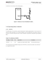
Page 53: ...indicating the module operation status You can connect it to a GPIO of DTE with pulled up or as LED indication circuit as below When the module is turned on normally the STATUS will present the low st...

Page 54: ...for judging whether the module is in sleep mode or not When the module enters into the sleep mode the SLEEP_IND will output a logic high level So you can use the SLEEP_IND for low current indication...

Page 55: ...ior No matter which port URC is presented on URC will trigger the behavior on RI pin URC can be output from UART port USB AT port and USB modem port by command AT QURCCFG The default port is USB AT po...

Page 56: ...mm gpsOneXTRA technology one kind of A GNSS which will download XTRA file from the internet server to enhance the TTFF XTRA file contains predicted GPS and GLONASS satellites coordinates and clock bia...

Page 57: ...32 s XTRA enabled 22 s Warm start open sky Autonomous 29 s XTRA enabled 3 s Hot start open sky Autonomous 2 5 s XTRA enabled 2 s Accuracy GNSS CEP 50 Autonomous open sky 1 5 m 1 Tracking sensitivity...

Page 58: ...GNSS antenna and the main UMTS antenna Noisy digital circuits such as the USIM card USB interface Camera module Display connector and SD card should be away from the antenna Use ground vias around th...

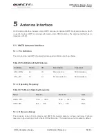
Page 59: ...Rx diversity antenna pins definition are shown below Table 25 Pin Definition of the RF Antenna Pin Name Pin No I O Description Comment ANT_MAIN 49 IO Main antenna 50 impedance ANT_DIV 35 AI Diversity...

Page 60: ...f Antenna Interface Keep a proper distance between main antenna and diversity antenna to improve the receiving sensitivity 5 2 GNSS Antenna Interface The following tables show the GNSS antenna pin def...

Page 61: ...ble 28 GNSS Frequency Type Frequency Unit GPS 1575 42 1 023 MHz GLONASS 1597 5 1605 8 MHz 5 2 1 Reference Design for Passive Antenna Passive antenna MAX2659 Module ANT_GNSS SHDN GND RFIN GND RFOUT VCC...

Page 62: ...ded LNA chip You can disable LNA to save power with one GPIO shown in above figure Pay attention to this pin s voltage level 3 VDD supplies power for active antenna You can choose the right VDD accord...

Page 63: ...ntenna noise figure 1 5dB Active antenna gain 2dBi Active antenna embedded LNA gain 20dB Typ Active antenna total gain 18dBi Typ 5 3 2 Install the Antenna with RF Connector The following figure is the...

Page 64: ...rdware_Design Confidential Released 63 84 Figure 38 Mechanicals of UF L LP Connectors The following figure describes the space factor of mated connector Figure 39 Space Factor of Mated Connector Unit...

Page 65: ...Absolute maximum ratings for power supply and voltage on digital and analog pins of module are listed in the following table Table 30 Absolute Maximum Ratings Parameter Min Max Unit VBAT_RF VBAT_BB 0...

Page 66: ...rating Temperature The operating temperature is listed in the following table Table 32 Operating Temperature Parameter Min Typ Max Unit Normal Temperature 35 25 75 C Restricted Operation1 40 35 75 85...

Page 67: ...sconnected DRX 6 14 0 mA Idle USB connected DRX 6 33 4 mA WCDMA data transfer GNSS off UMTS Band I HSDPA max power 517 mA UMTS Band I HSUPA max power 497 mA UMTS Band II HSDPA max power 521 mA UMTS Ba...

Page 68: ...Sensitivity The following table shows the conducted RF receiving sensitivity of UC20 module Table 35 Conducted RF Receiving Sensitivity Frequency Receive Sensitivity Typ UMTS 1900 110dBm UMTS 850 110d...

Page 69: ...are Design UC20_Hardware_Design Confidential Released 68 84 Table 36 Electrostatics Discharge Characteristics Tested Points Contact Discharge Air Discharge Unit VBAT GND 5 10 kV All antenna interfaces...

Page 70: ...are_Design Confidential Released 69 84 7 Mechanical Dimensions This chapter describes the mechanical dimensions of the module All dimensions are measured in mm 7 1 Mechanical Dimensions of the Module...

Page 71: ...Hardware Design UC20_Hardware_Design Confidential Released 70 84 3 4 3 2 3 4 3 2 3 4 3 2 4 8 32 29 0 5 1 5 Figure 41 UC20 Bottom Dimensions Bottom View XXXX in pink on above figure is the PCB board co...

Page 72: ...UMTS HSPA Module Series UC20 Hardware Design UC20_Hardware_Design Confidential Released 71 84 Figure 42 Bottom Pads Dimensions Bottom View...

Page 73: ...1 9 7 8 13 1 9 9 04 9 3 6 45 3 45 4 4 22 1 6 16 29 0 8 1 3 4 8 2 3 4 6 2 5 1 0 3 4 6 8 Figure 43 Recommended Footprint Top View 1 Keep out the area below the test point circular area on the above figu...

Page 74: ...Module Series UC20 Hardware Design UC20_Hardware_Design Confidential Released 73 84 7 3 Top View of the Module Figure 44 Top View of the Module 7 4 Bottom View of the Module Figure 45 Bottom View of t...

Page 75: ...ore than 72 hours at factory conditions of o30 C 60 RH If baking is required devices may be baked for 48 hours at 125 C 5 C As plastic container cannot be subjected to high temperature Module needs to...

Page 76: ...d that the module should be mounted after the first panel has been reflowed The following picture is the actual diagram which we have operated Time 50 100 150 200 250 300 50 100 150 200 250 160 C 200...

Page 77: ...fidential Released 76 84 30 3 0 15 29 3 0 15 30 3 0 15 32 5 0 15 33 5 0 15 0 35 0 05 4 2 0 15 3 1 0 15 32 5 0 15 33 5 0 15 4 00 0 1 2 00 0 1 1 75 0 1 20 20 0 15 44 00 0 3 44 00 0 1 1 50 0 1 Direction...

Page 78: ...gn UC20 and M10 Compatible Reference Design 5 UC20 M10_Compatibilty_Design UC20 and M10 Compatibility Design Specification 6 Module_Secondary_SMT_User_Guide Module Secondary SMT User Guide 7 UC20_GNSS...

Page 79: ...nikovaya Sistema the Russian Global Navigation Satellite System GMSK Gaussian Minimum Shift Keying GNSS Global Navigation Satellite System GPS Global Positioning System GSM Global System for Mobile Co...

Page 80: ...an Square value RTC Real Time Clock Rx Receive SIM Subscriber Identification Module SMS Short Message Service TDMA Time Division Multiple Access TE Terminal Equipment TX Transmitting Direction UART Un...

Page 81: ...n Minimum Input Low Level Voltage Value VImax Absolute Maximum Input Voltage Value VImin Absolute Minimum Input Voltage Value VOHmax Maximum Output High Level Voltage Value VOHmin Minimum Output High...

Page 82: ...UMTS HSPA Module Series UC20 Hardware Design UC20_Hardware_Design Confidential Released 81 84...

Page 83: ...UMTS HSPA Module UC20 Hardware Design UC20_Hardware_Design Confidential Released 82 84...

Reviews: