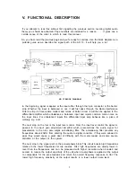
The branch in the road after the pre-emphasis leads to a dead end at the headroom meter,
which must be attached after the pre-emphasis is applied to the input signal so that a visual
indication of what is really being applied to the digital converter can be monitored. Up the
other fork lies the sample and hold circuit. This clever trick provides the converter with a
steady voltage during the conversion process. To do this, the sample and hold actually holds
the input voltage steady during each sample cycle, releasing the input only after a digital
reading is completed. Once the sample is complete, the sample and hold takes another look at
the input and then freezes the voltage at a new level.
The analog samples provided by the sample and hold then pass on to the input stage of the
analog to digital converter. Unlike the example which was required reading on the previous
page, the converter in the AD 13 runs at a 50kHz sample rate (just to be sure). It will then
produce a binary number in the range of 0 to 16,383 (no, this is not binary; binary would be “in
the range of 00000000000000 to 11111111111111”), at every 1/50,000 second interval.
At this point the signal path disappears into some murky pool casually labelled “Digital Signal
Processing” in the block diagram. It is into this mystical madness that the front panel control
switches are connected as well as the display, and the three digital to analog output
converters.
The memory which provides the delay is found in this block, along with the CPU (central
processing unit, or computer for short) and several housekeeping circuits which are necessary
to keep the lines from getting tangled at the 16,000,000 cycle speed of the CPU. AII of the data
coming into the block from the analog-to-digital converter is written to memory, and is made
available for recall at any 20 microsecond real time interval from 0 to 654 milliseconds after it
has been stored. All three of the digital to analog converters has access to the data at any time
within the boundaries of the maximum delay.
The front panel switches are connected to the CPU as is the display and the memory. Switch
closures tell the digital-to-analog converters where to look for the appropriate data to provide
the amount of delay indicated on the display. Leaving out all of the details is really quite
necessary. You see, we have a certain budget for the printing and handling of these owner’s
manuals and the amount of paper and ink it would take to go beyond these limits would be
prohibitive.
Data is clocked out of the digital processing block to the three digital to analog converters in an
appropriate manner to reconstruct a replica of the original analog input, plus time delay, if any.
The reconstructed audio is actually a series of steps identical to the steps which appeared at
the output of the sample and hold. At this point in the signal path lies the de-emphasis circuit
which removes the frequency shaping that was applied to the signal before conversion to the
digital domain. The aforementioned steps in the audio are then removed with another nine
pole elliptical filter. All of the frequency components of these steps are higher in frequency
than the cutoff frequency of the filter. At the output of the filters there is a buffer amplifier
which scales the gain appropriately and drives the output level control pot.
After this processing, the signal is subjected to a pair of amplifiers which either directly drives
the outputs in an active balanced or unbalanced fashion or through a switch selectable output
coupling transformer. The very last item of importance is the bypass relay. This relay must be
energized by the CPU for any delayed signal to be present at the output. During warm-up and
power off conditions the relay is in its resting position which diverts all input signals directly to
the output connectors.
8


