22
After 4 minutes of continuous transmit, the RAY 210 will emit two warning
tones. If the transmitter remains engaged for an additional minute, or 5 minutes
total, the RAY 210 will automatically disable the transmit
operation.
At this time, the RAY 210 will cease transmitting, emit an alarm, and “ot” will
be displayed on the LCD. To return to normal operation, the microphone FIT
switch must be disengaged.
3.3.7 To Transmit and Receive on INTL Frequencies
To transmit and receive on International frequencies, press the [FUNC] and then
the [INTL] key, then select the desired channel. INTL will appear on the display
to indicate International operation.
3.3.8 Selecting a Weather Channel
To select and receive a weather channel, press the [WX] key and then rotate the
channel selector switch to the desired channel (0-9). Refer to the below Table 3-
1 for specific weather channel frequencies. When in the weather mode, the
transmitter is disabled.
Channel
Frequency (MHz)
Type Traffic
Function-Ship to Shore
WX0
163.275
NOAA Weather
Receive Only
WX1
162.550
NOAA Weather
Receive Only
WX2
162.400
NOAA Weather
Receive Only
WX3
162.475
NOAA Weather
Receive Only
WX4
162.425
NOAA Weather
Receive Only
WX5
162.450
NOAA Weather
Receive Only
WX6
162.500
NOAA Weather
Receive Only
WX7
162.525
NOAA Weather
Receive Only
WX8
161.650
Canadian Weath.
Receive Only
WX9
161.775
Canadian Weath.
Receive Only
Table 3-1 RAY 210 VHF WEATHER CHANNELS AND FREQUENCIES
Summary of Contents for RAY 210VHF
Page 2: ......
Page 3: ......
Page 4: ......
Page 6: ......
Page 8: ......
Page 10: ......
Page 12: ......
Page 19: ...7 Figure 2 2 Outline and Mounting Dimensions...
Page 30: ...18 Figure 3 1 Layout of Controls and Connectors...
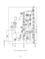
Page 40: ...28 Fig 4 1 Block Diagram RF PCB...
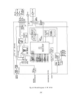
Page 41: ...29 Fig 4 2 Block Diagram CPU PCB...
Page 55: ...43 6 2 RAY210 ASSEMBLY DRAWING...
Page 57: ...45 6 3 SCHEMATIC DIAGRAM Fig 6 1 Schematic diagram RF PCB...
Page 58: ...46 Fig 6 2 Schematic diagram CPU PCB l...
Page 59: ...47 Fig 6 2 Schematic diagram CPU PCB 2...
Page 60: ...48 Fig 6 3 RF PCB Layout Top View...
Page 61: ...49 Fig 6 4 RF PCB Layout Rear View...
Page 62: ...50 Fig 6 5 CPU PCB Layout Top view...
Page 63: ...51 Fig 6 5 CPU PCB Layout Rear View...
Page 64: ...52...
Page 75: ...63...


