BR200D-U1/BR300D-U1
Service Manual
25
The audio signals after demodulation in IC200 may contain CTCSS (continuous tone control squelch
system) or DCS
(
digital squelch
)
signals. The spectrum component of CTCSS/DCS is 67 to 250Hz. The
filtering circuit composed of IC301 can filter out signals except CTCSS/DCS spectrum, which makes
MCU decode the CTCSS/DCS more accurately.
5.3 Transmitter (Tx)
Transmitter Power Amplifier
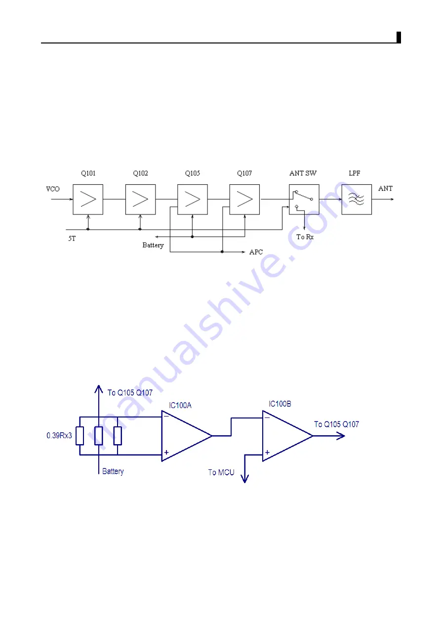
Figure 4 Schematic Diagram for Power Amplifier and Antenna Switch
The modulated RF signals from VCO are amplified by Q101, Q102 and Q105 before the power
amplification in Q107.
Gate bias of Q105 and Q107 is controlled by APC circuit, so the output power of transmitter can be
controlled conveniently by changing the gate bias voltage.
APC
(
Automatic Power Control
)
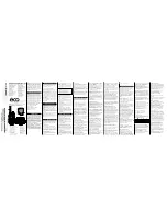
Figure 5 Schematic Diagram for APC Circuit
R130 R131 and R132 are power amplification current detector, IC100A is power amplification current
sampling amplifier and IC00B is power comparison amplifier.
The power amplification current and IC100A output will increase with oversized output power of
transmitter. When the output voltage of IC100B decreases, the bias voltage of Q105 and Q107 will
Summary of Contents for BR200D-U1
Page 1: ...BR200D U1 BR300D U1 Service Manual 1 BR200D U1 BR300D U1 Service Manual ...
Page 17: ...BR200D U1 BR300D U1 Service Manual 17 Exploded View of the Parts ...
Page 20: ...BR200D U1 BR300D U1 Service Manual 20 DR7000 2 ...
Page 36: ...BR200D U1 BR300D U1 Service Manual 36 Chapter 6 PCB Layout ...
Page 37: ...MIC1 C5 D4 D5 D8 C4 C3 R1 D2 D3 D6 C7 C8 C9 J1 D1 D9 C2 D7 C6 C13 C1 ...
Page 70: ...BR200D U1 BR300D U1 Service Manual 66 Chapter 10 Block and Schematic ...


