R01UH0823EJ0100 Rev.1.00
Page 1614 of 1823
Jul 31, 2019
RX23W Group
44. 12-Bit A/D Converter (S12ADE)
44.7
Allowable Impedance of Signal Source
To achieve high-speed conversion of 0.83 μs, the analog input pins of this MCU are designed so that the conversion
accuracy is guaranteed if the impedance of the input signal source is 0.5 kΩ or less. If an external capacitor of large
capacitance is attached in the application in which only a single pin input is converted in single scan mode, the only load
on input is virtually 2.6 kΩ of the internal input resistor; therefore, the impedance of the signal source can be ignored.
Being a low-pass filter, however, an analog input circuit may not follow the analog signal with a large differential
coefficient. When high-speed analog signals are to be converted or multiple pins are to be converted in scan mode, a low-
impedance buffer should be used.
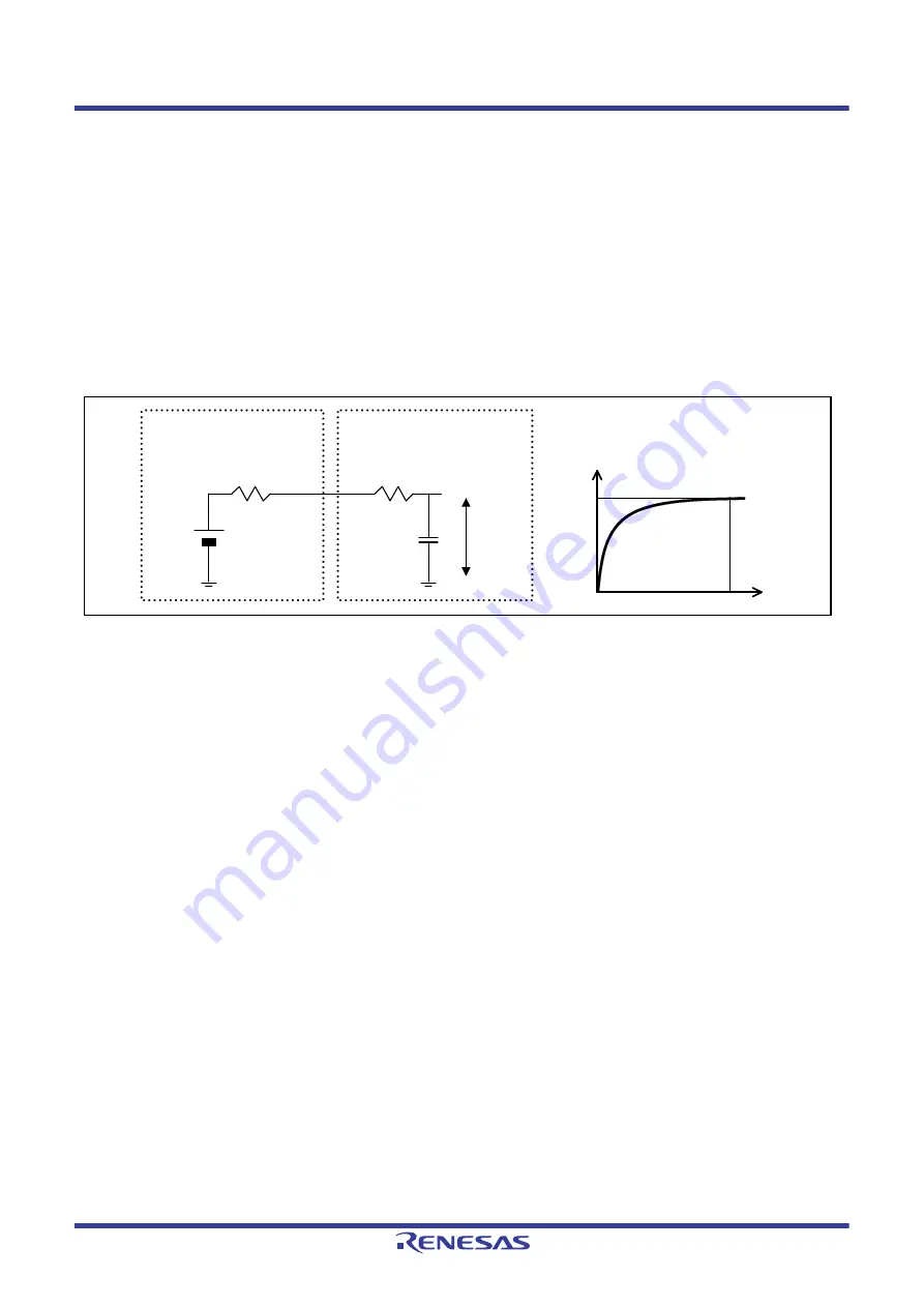
shows an equivalent circuit of an analog input pin and an external sensor.
To perform A/D conversion accurately, charging of the internal capacitor C shown in
must be completed
within the specified period of time. This specified period is referred to as sampling time.
Figure 44.28
Equivalent Circuit of Analog Input Pin and External Sensor
VC
VIN
t
VIN
R0
Sensor equivalent circuit
C
R


