R01UH0823EJ0100 Rev.1.00
Page 98 of 1823
Jul 31, 2019
RX23W Group
3. Operating Modes
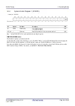
3.2.2
System Control Register 1 (SYSCR1)
Note:
Set the PRCR.PRC1 bit to 1 (write enabled) before rewriting this register.
RAME Bit (RAM Enable)
The RAME bit enables or disables the RAM.
A 0 should not be written to this bit during access to the RAM. When accessing the RAM immediately after changing the
RAME bit from 0 (RAM disabled) to 1 (RAM enabled), make sure that the RAME bit is 1 before the access.
Even when the RAME bit is cleared to 0, the RAM retains its value. To retain the value in the RAM, keep the specified
RAM standby voltage (VRAM). For details, see
section 51, Electrical Characteristics
.
Address(es): 0008 0008h
b15
b14
b13
b12
b11
b10
b9
b8
b7
b6
b5
b4
b3
b2
b1
b0
—
—
—
—
—
—
—
—
—
—
—
—
—
—
—
RAME
Value after reset:
0
0
0
0
0
0
0
0
0
0
0
0
0
0
0
1
Bit
Symbol
Bit Name
Description
R/W
b0
RAM Enable
0: The RAM is disabled.
1: The RAM is enabled.
R/W
b15 to b1
—
Reserved
These bits are read as 0. The write value should be 0.
R/W


