background image

R01UH0823EJ0100 Rev.1.00

Page 1491 of 1823

Jul 31, 2019

RX23W Group

43. Capacitive Touch Sensing Unit (CTSU)

43.1

Overview

Table 43.1

 lists the specifications of the CTSU, an

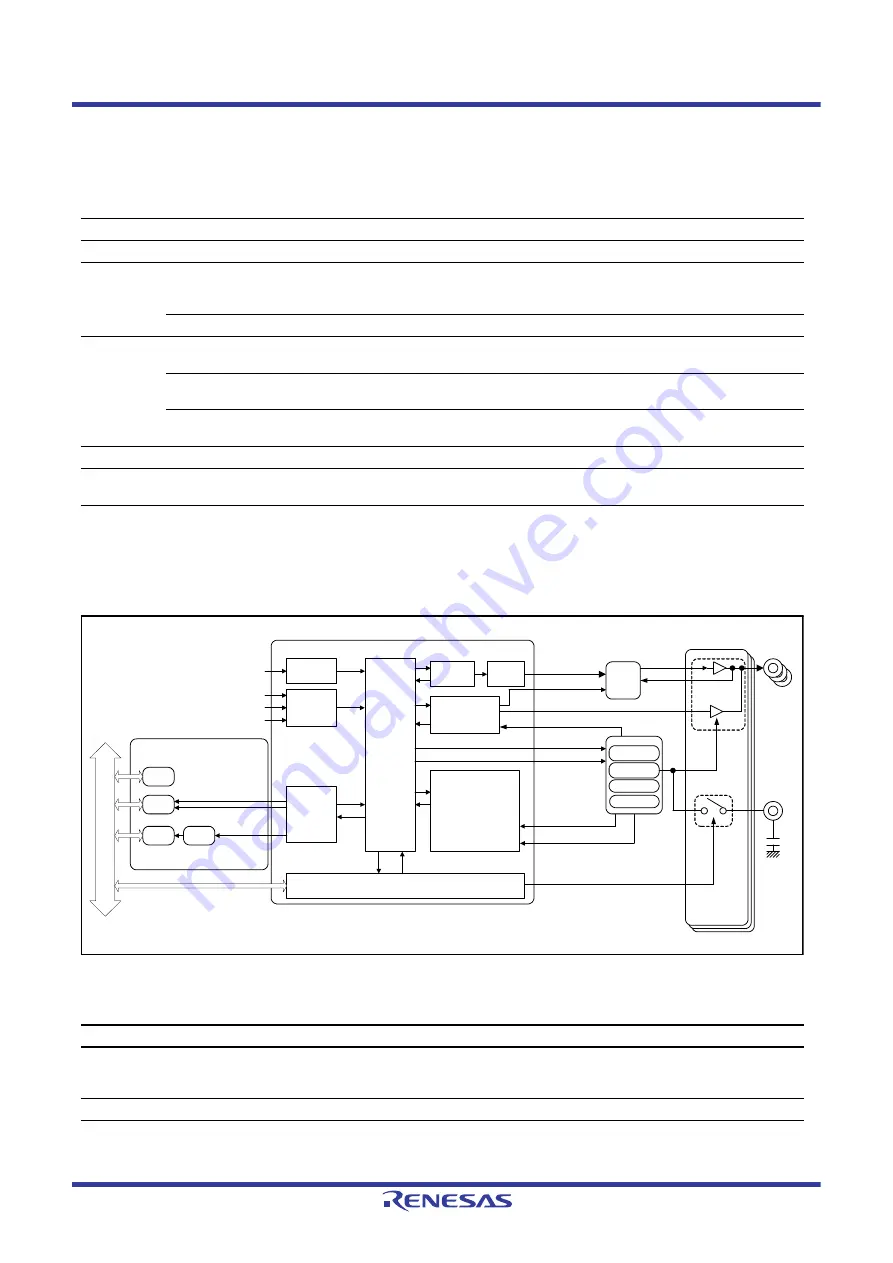
Figure 43.3

 shows a block diagram of the CTSU.

As shown in 

Figure 43.3

, the CTSU consists of the status control block, trigger control block, clock control block, 

channel control block, port control block, sensor drive pulse generator, measurement block, interrupt block, and control 
registers.

Figure 43.3

CTSU Block Diagram (m = 2, 3, 4, 7, 8, 12, 13, 22, 23, 27, 30, 35)

Table 43.1

CTSU Specifications

Item

Description

Operating clock

PCLK, PCLK/2, or PCLK/4

Pins

TS2, TS3, TS4, TS7, TS8, TS12, 
TS13, TS22, TS23, TS27, TS30, 
TS35

Electrostatic capacitance measurement pins (12 channels)

TSCAP

LPF (low-pass filter) connection pin

Measurement 
modes

Self-capacitance single scan 
mode

Electrostatic capacitance on a channel is measured by the self-capacitance 
method.

Self-capacitance multi-scan mode Electrostatic capacitance on multiple channels is measured successively by the 

self-capacitance method.

Mutual capacitance full scan 
mode

Electrostatic capacitance on multiple channels is measured successively by 
mutual capacitance.

Noise prevention

Synchronous noise prevention, high-pass noise prevention

Measurement start conditions

Software trigger

External trigger (event input from the event link controller (ELC))

Table 43.2

CTSU Pin Configuration

Pin Name

I/O

Function

TS2, TS3, TS4, TS7, TS8, TS12, 
TS13, TS22, TS23, TS27, TS30, 
TS35

I/O

Electrostatic capacitive measurement pins (touch pins)

TSCAP

LPF connection pin

System control block

Trigger

control block

Status

control

Capacitive touch sensing unit (CTSU)

Channel

control block

PCLK

PCLK/2
PCLK/4

Event input from event link

controller (ELC)

Port

control

Measurement block

(counter measurement)

• CTSUSC counter
• CTSURC counter

Clock

control

block

Sensor drive

pulse generator

Interrupt

block

Port control

Sensor drive pulse

Operation enable

Control registers

Offset control

Sensor ICO clock

Reference ICO clock

Port

control

block

Power
supply

DTC

CTSURD interrupt request

D

at

a

 bus

Memory

CTSUWR interrupt request

CPU

ICU

CTSUFN

interrupt request

Diffusion clock

Count 

source

H/M

Sensor ICO

Reference ICO

Power supply

control

Diffusion clock

Touch I/O

I/O block

TSCAP

LPF

TSCAP I/O

TSm

ICO: Current-Controlled Oscillator

Summary of Contents for RX Series

Page 1: ...se materials including products and product specifications represents information on the product at the time of publication and is subject to change by Renesas Electronics Corp without notice Please review the latest information published by Renesas Electronics Corp through various means including the Renesas Electronics Corp website http www renesas com Cover ...

Page 2: ...onics with respect to maximum ratings operating power supply voltage range heat dissipation characteristics installation etc Renesas Electronics disclaims any and all liability for any malfunctions failure or accident arising out of the use of Renesas Electronics products outside of such specified ranges 7 Although Renesas Electronics endeavors to improve the quality and reliability of Renesas Ele...

Page 3: ...put signal during power off state as described in your product documentation 4 Handling of unused pins Handle unused pins in accordance with the directions given under handling of unused pins in the manual The input pins of CMOS products are generally in the high impedance state In operation with an unused pin in the open circuit state extra electromagnetic noise is induced in the vicinity of the ...

Page 4: ...r contexts and at the final part of each section and in the section giving usage notes The list of revisions is a summary of major points of revision or addition for earlier versions It does not cover all revised items For details on the revised points see the actual locations in the manual Document Type Contents Document Title Document No Datasheet Overview of hardware and electrical characterist...

Page 5: ... bit or field is readable Writing to this bit or field has no effect 2 Reserved Use the specified value when writing to this bit or field otherwise the correct operation is not guaranteed 3 Setting prohibited The correct operation is not guaranteed if such a setting is performed X X X Register Address es xxxx xxxxh b7 b6 b5 b4 b3 b2 b1 b0 1 0 4 0 Value after reset x 0 0 0 0 0 0 0 x Undefined Bit S...

Page 6: ...dancy Check DMA Direct Memory Access DMAC Direct Memory Access Controller GSM Global System for Mobile Communications Hi Z High Impedance IEBus Inter Equipment Bus I O Input Output IrDA Infrared Data Association LSB Least Significant Bit MSB Most Significant Bit NC Non Connect PLL Phase Locked Loop PWM Pulse Width Modulation SIM Subscriber Identity Module UART Universal Asynchronous Receiver Trans...

Page 7: ... PC BPC 74 2 2 2 7 Backup PSW BPSW 75 2 2 2 8 Fast Interrupt Vector Register FINTV 75 2 2 2 9 Floating Point Status Word FPSW 76 2 2 3 Accumulator 78 2 3 Processor Mode 79 2 3 1 Supervisor Mode 79 2 3 2 User Mode 79 2 3 3 Privileged Instruction 79 2 3 4 Switching Between Processor Modes 79 2 4 Data Types 80 2 4 1 Integer 80 2 4 2 Floating Points 81 2 4 3 Bitwise Operations 81 2 4 4 Strings 82 2 5 ...

Page 8: ... Single Chip Mode 99 3 3 2 Boot Mode 99 3 3 2 1 Boot Mode USB Interface 99 3 3 2 2 Boot Mode SCI 99 3 4 Transitions of Operating Modes 100 3 4 1 Operating Mode Transitions Determined by the Mode Setting Pins 100 4 Address Space 101 4 1 Address Space 101 5 I O Registers 103 5 1 I O Register Addresses Address Order 105 6 Resets 136 6 1 Overview 136 6 2 Register Descriptions 138 6 2 1 Reset Status Re...

Page 9: ...63 8 4 Reset from Voltage Monitor 0 164 8 5 Interrupt and Reset from Voltage Monitoring 1 165 8 6 Event Link Output 167 8 6 1 Interrupt Handling and Event Linking 167 9 Clock Generation Circuit 168 9 1 Overview 168 9 2 Register Descriptions 172 9 2 1 System Clock Control Register SCKCR 172 9 2 2 System Clock Control Register 3 SCKCR3 174 9 2 3 PLL Control Register PLLCR 175 9 2 4 PLL Control Regis...

Page 10: ...lator 198 9 4 1 Connecting 32 768 kHz Crystal 198 9 4 2 Handling of Pins When Sub Clock is Not Used 199 9 5 Dedicated Clock Oscillator for Bluetooth 200 9 5 1 Connecting the Oscillator 200 9 5 2 Connecting the Bluetooth Dedicated Clock Output Pin 200 9 6 Oscillation Stop Detection Function 201 9 6 1 Oscillation Stop Detection and Operation after Detection 201 9 6 2 Oscillation Stop Detection Inter...

Page 11: ...ptions 225 11 2 1 Standby Control Register SBYCR 225 11 2 2 Module Stop Control Register A MSTPCRA 226 11 2 3 Module Stop Control Register B MSTPCRB 227 11 2 4 Module Stop Control Register C MSTPCRC 229 11 2 5 Module Stop Control Register D MSTPCRD 230 11 2 6 Operating Power Control Register OPCCR 231 11 2 7 Sub Operating Power Control Register SOPCCR 232 11 2 8 Sleep Mode Return Clock Source Swit...

Page 12: ...on 253 12 3 1 Battery Backup Function 253 12 3 2 VBATT Pin Voltage Monitoring Function 254 12 4 Usage Notes 255 13 Register Write Protection Function 256 13 1 Register Descriptions 257 13 1 1 Protect Register PRCR 257 14 Exception Handling 258 14 1 Exception Events 258 14 1 1 Undefined Instruction Exception 259 14 1 2 Privileged Instruction Exception 259 14 1 3 Access Exceptions 259 14 1 4 Floatin...

Page 13: ... IRQCRi i 0 1 and 4 to 7 277 15 2 9 IRQ Pin Digital Filter Enable Register 0 IRQFLTE0 278 15 2 10 IRQ Pin Digital Filter Setting Register 0 IRQFLTC0 279 15 2 11 Non Maskable Interrupt Status Register NMISR 280 15 2 12 Non Maskable Interrupt Enable Register NMIER 282 15 2 13 Non Maskable Interrupt Status Clear Register NMICLR 284 15 2 14 NMI Pin Interrupt Control Register NMICR 285 15 2 15 NMI Pin ...

Page 14: ...ERCLR 311 16 3 2 Bus Error Monitoring Enable Register BEREN 311 16 3 3 Bus Error Status Register 1 BERSR1 312 16 3 4 Bus Error Status Register 2 BERSR2 312 16 3 5 Bus Priority Control Register BUSPRI 313 16 4 Bus Error Monitoring Section 315 16 4 1 Types of Bus Error 315 16 4 1 1 Illegal Address Access 315 16 4 1 2 Timeout 315 16 4 2 Operations When a Bus Error Occurs 316 16 4 3 Conditions Leading...

Page 15: ...Setting Access Control Information 336 17 4 2 Enabling Memory Protection 336 17 4 3 Transition to User Mode 336 17 4 4 Processing in Response to Memory Protection Errors 336 18 DMA Controller DMACA 338 18 1 Overview 338 18 2 Register Descriptions 340 18 2 1 DMA Source Address Register DMSAR 340 18 2 2 DMA Destination Address Register DMDAR 340 18 2 3 DMA Transfer Count Register DMCRA 341 18 2 4 DM...

Page 16: ...he End of each Transfer 378 18 8 5 Setting of DMAC Activation Source Select Register of the Interrupt Controller ICU DMRSRm 378 18 8 6 Suspending or Restarting DMA Activation 378 19 Data Transfer Controller DTCa 379 19 1 Overview 379 19 2 Register Descriptions 381 19 2 1 DTC Mode Register A MRA 381 19 2 2 DTC Mode Register B MRB 382 19 2 3 DTC Transfer Source Register SAR 383 19 2 4 DTC Transfer D...

Page 17: ... Register n ELSRn n 1 to 4 7 8 10 12 14 to 16 18 to 29 412 20 2 3 Event Link Option Setting Register A ELOPA 415 20 2 4 Event Link Option Setting Register B ELOPB 415 20 2 5 Event Link Option Setting Register C ELOPC 416 20 2 6 Event Link Option Setting Register D ELOPD 416 20 2 7 Port Group Setting Register n PGRn n 1 2 417 20 2 8 Port Group Control Register n PGCn n 1 2 418 20 2 9 Port Buffer Re...

Page 18: ...otect Register PWPR 457 22 2 2 P0n Pin Function Control Register P0nPFS n 3 5 7 458 22 2 3 P1n Pin Function Control Registers P1nPFS n 4 to 7 459 22 2 4 P2n Pin Function Control Register P2nPFS n 1 2 5 to 7 460 22 2 5 P3n Pin Function Control Registers P3nPFS n 0 1 461 22 2 6 P4n Pin Function Control Registers P4nPFS n 0 to 7 462 22 2 7 PBn Pin Function Control Registers PBnPFS n 0 1 3 5 7 463 22 ...

Page 19: ...put Control Registers 1 TOCR1 504 23 2 18 Timer Output Control Registers 2 TOCR2 506 23 2 19 Timer Output Level Buffer Registers TOLBR 508 23 2 20 Timer Gate Control Registers TGCR 509 23 2 21 Timer Subcounters TCNTS 510 23 2 22 Timer Dead Time Data Registers TDDR 510 23 2 23 Timer Cycle Data Registers TCDR 511 23 2 24 Timer Cycle Buffer Registers TCBR 511 23 2 25 Timer Interrupt Skipping Set Regi...

Page 20: ...1 23 6 13 Counter Value When Count Operation is Stopped in Complementary PWM Mode 602 23 6 14 Buffer Operation Setting in Complementary PWM Mode 602 23 6 15 Buffer Operation and Compare Match Flags in Reset Synchronized PWM Mode 603 23 6 16 Overflow Flags in Reset Synchronized PWM Mode 604 23 6 17 Contention between Overflow Underflow and Counter Clearing 605 23 6 18 Contention between TCNT Write ...

Page 21: ...on 653 24 3 2 Output Level Compare Operation 654 24 3 3 High Impedance Control Using Registers 655 24 3 4 High Impedance Control on Detection of Stopped Oscillation 655 24 3 5 High Impedance Control in Response to Receiving an Event Signal from the ELC 655 24 3 6 Release from the High Impedance 655 24 4 Interrupts 656 24 5 Usage Notes 656 24 5 1 Transitions to Software Standby Mode 656 24 5 2 When...

Page 22: ...lict between TPUm TCNT Write and Increment Operations 717 25 9 6 Conflict between TPUm TGRy Write and Compare Match 718 25 9 7 Conflict between Buffer Register Write and Compare Match 718 25 9 8 Conflict between TPUm TGRy Read and Input Capture 719 25 9 9 Conflict between TPUm TGRy Write and Input Capture 719 25 9 10 Conflict between Buffer Register Write and Input Capture 720 25 9 11 TCNT Simulta...

Page 23: ...DTC Activation 746 26 7 Link Operation by ELC 747 26 7 1 Event Signal Output to ELC 747 26 7 2 TMR Operation when Receiving an Event Signal from ELC 747 26 7 3 Notes on Operating TMR According to an Event Signal from ELC 748 26 8 Usage Notes 749 26 8 1 Module Stop State Setting 749 26 8 2 Notes on Setting Cycle 749 26 8 3 Conflict between TCNT Write and Counter Clear 749 26 8 4 Conflict between TC...

Page 24: ...2 767 28 2 5 Day of Week Counter RWKCNT Binary Counter 3 BCNT3 768 28 2 6 Date Counter RDAYCNT 769 28 2 7 Month Counter RMONCNT 770 28 2 8 Year Counter RYRCNT 771 28 2 9 Second Alarm Register RSECAR Binary Counter 0 Alarm Register BCNT0AR 772 28 2 10 Minute Alarm Register RMINAR Binary Counter 1 Alarm Register BCNT1AR 773 28 2 11 Hour Alarm Register RHRAR Binary Counter 2 Alarm Register BCNT2AR 77...

Page 25: ...8 2 Adjustment by Software 798 28 3 8 3 Procedure for Changing the Mode of Adjustment 799 28 3 8 4 Procedure for Stopping Adjustment 799 28 3 8 5 Capturing the Time 800 28 4 Interrupt Sources 801 28 5 Event Link Output 803 28 5 1 Interrupt Handling and Event Linking 803 28 6 Usage Notes 804 28 6 1 Register Writing during Counting 804 28 6 2 Use of Periodic Interrupts 804 28 6 3 RTCOUT 1 Hz 64 Hz C...

Page 26: ...Mode 827 30 3 1 1 Register Start Mode 827 30 3 1 2 Auto Start Mode 829 30 3 2 Control over Writing to the WDTCR and WDTRCR Registers 831 30 3 3 Refresh Operation 831 30 3 4 Reset Output 832 30 3 5 Interrupt Source 832 30 3 6 Reading the Down Counter Value 833 30 3 7 Correspondence between Option Function Select Register 0 OFS0 and WDT Registers 833 31 Independent Watchdog Timer IWDTa 834 31 1 Over...

Page 27: ...ntrol Register CFIFOCTR D0FIFO Port Control Register D0FIFOCTR D1FIFO Port Control Register D1FIFOCTR 867 32 2 7 Interrupt Enable Register 0 INTENB0 869 32 2 8 Interrupt Enable Register 1 INTENB1 870 32 2 9 BRDY Interrupt Enable Register BRDYENB 871 32 2 10 NRDY Interrupt Enable Register NRDYENB 872 32 2 11 BEMP Interrupt Enable Register BEMPENB 873 32 2 12 SOF Output Configuration Register SOFCFG...

Page 28: ... 912 32 3 1 4 Example of USB External Connection Circuit 913 32 3 2 Interrupt Sources 920 32 3 3 Interrupt Descriptions 922 32 3 3 1 BRDY Interrupt 922 32 3 3 2 NRDY Interrupt 926 32 3 3 3 BEMP Interrupt 929 32 3 3 4 Device State Transition Interrupt 930 32 3 3 5 Control Transfer Stage Transition Interrupt 931 32 3 3 6 Frame Update Interrupt 932 32 3 3 7 VBUS Interrupt 932 32 3 3 8 Resume Interrup...

Page 29: ...32 3 9 1 Error Detection in Isochronous Transfers 946 32 3 9 2 Data PID 947 32 3 9 3 Interval Counter 947 32 3 10 SOF Interpolation Function 954 32 3 11 Pipe Schedule 955 32 3 11 1 Conditions for Generating a Transaction 955 32 3 11 2 Transfer Schedule 955 32 3 11 3 Enabling USB Communication 955 32 4 Usage Notes 956 32 4 1 Setting the Module Stop Function 956 32 5 Battery Charging Detection Proce...

Page 30: ... 29 Control Field 0 Data Register CF0DR 1013 33 2 30 Control Field 0 Compare Enable Register CF0CR 1014 33 2 31 Control Field 0 Receive Data Register CF0RR 1014 33 2 32 Primary Control Field 1 Data Register PCF1DR 1014 33 2 33 Secondary Control Field 1 Data Register SCF1DR 1015 33 2 34 Control Field 1 Compare Enable Register CF1CR 1015 33 2 35 Control Field 1 Receive Data Register CF1RR 1015 33 2 ...

Page 31: ... Output Control 1060 33 7 Operation in Simple I2C Mode 1061 33 7 1 Generation of Start Restart and Stop Conditions 1062 33 7 2 Clock Synchronization 1064 33 7 3 SSDA Output Delay 1065 33 7 4 SCI Initialization Simple I2C Mode 1066 33 7 5 Operation in Master Transmission Simple I2C Mode 1067 33 7 6 Master Reception Simple I2C Mode 1069 33 7 7 Recovery from Bus Hang up 1071 33 8 Operation in Simple ...

Page 32: ...Clock Synchronous Transmission Clock Synchronous Mode and Simple SPI Mode 1099 33 14 7 Restrictions on Using DMAC or DTC 1100 33 14 8 Notes on Starting Transfer 1100 33 14 9 SCI Operations during Low Power Consumption State 1100 33 14 10 External Clock Input in Clock Synchronous Mode and Simple SPI Mode 1103 33 14 11 Limitations on Simple SPI Mode 1104 33 14 12 Limitation 1 on Usage of the Extende...

Page 33: ...ata Register ICDRT 1144 35 2 16 I2C bus Receive Data Register ICDRR 1144 35 2 17 I2C bus Shift Register ICDRS 1144 35 3 Operation 1145 35 3 1 Communication Data Format 1145 35 3 2 Initial Settings 1146 35 3 3 Master Transmit Operation 1147 35 3 4 Master Receive Operation 1150 35 3 5 Slave Transmit Operation 1156 35 3 6 Slave Receive Operation 1159 35 4 SCL Synchronization Circuit 1161 35 5 SDA Out...

Page 34: ...s Issued or a Condition is Detected 1187 35 15 Event Link Function Output 1188 35 15 1 Interrupt Handling and Event Linking 1188 35 16 Usage Notes 1189 35 16 1 Setting Module Stop Function 1189 35 16 2 Notes on Starting Transfer 1189 36 CAN Module RSCAN 1190 36 1 Overview 1190 36 2 Register Descriptions 1193 36 2 1 Bit Configuration Register L CFGL 1193 36 2 2 Bit Configuration Register H CFGH 119...

Page 35: ... 36 2 36 Receive FIFO Pointer Control Register m RFPCTRm m 0 1 1226 36 2 37 Receive FIFO Access Register mAL RFIDLm m 0 1 1227 36 2 38 Receive FIFO Access Register mAH RFIDHm m 0 1 1227 36 2 39 Receive FIFO Access Register mBL RFTSm m 0 1 1228 36 2 40 Receive FIFO Access Register mBH RFPTRm m 0 1 1228 36 2 41 Receive FIFO Access Register mCL RFDF0m m 0 1 1229 36 2 42 Receive FIFO Access Register m...

Page 36: ...F2p p 0 to 3 1254 36 2 73 Transmit Buffer Register pDH TMDF3p p 0 to 3 1254 36 2 74 Transmit History Buffer Control Register THLCC0 1255 36 2 75 Transmit History Buffer Status Register THLSTS0 1256 36 2 76 Transmit History Buffer Access Register THLACC0 1257 36 2 77 Transmit History Buffer Pointer Control Register THLPCTR0 1258 36 2 78 Global RAM Window Control Register GRWCR 1259 36 2 79 Global T...

Page 37: ...g Procedure 1298 36 12 2 Protection Unlock Procedure 1299 36 12 3 RAM Test Setting Procedure 1300 36 13 Notes on the CAN Module 1301 37 Serial Sound Interface SSI 1302 37 1 Overview 1302 37 2 Register Descriptions 1304 37 2 1 Control Register SSICR 1304 37 2 2 Status Register SSISR 1308 37 2 3 FIFO Control Register SSIFCR 1310 37 2 4 FIFO Status Register SSIFSR 1312 37 2 5 Transmit FIFO Data Regis...

Page 38: ...Overview of RSPI Operations 1358 38 3 2 Controlling RSPI Pins 1359 38 3 3 RSPI System Configuration Examples 1360 38 3 3 1 Single Master Single Slave with This MCU Acting as Master 1360 38 3 3 2 Single Master Single Slave with This MCU Acting as Slave 1361 38 3 3 3 Single Master Multi Slave with This MCU Acting as Master 1362 38 3 3 4 Single Master Multi Slave with This MCU Acting as Slave 1363 38...

Page 39: ...inking 1410 38 4 1 Receive Buffer Full Event Output 1410 38 4 2 Transmit Buffer Empty Event Output 1410 38 4 3 Mode Fault Overrun or Parity Error Event Output 1410 38 4 4 RSPI Idle Event Output 1411 38 4 5 Transmission Completed Event Output 1411 38 5 Usage Notes 1412 38 5 1 Setting Module Stop Function 1412 38 5 2 Note on Low Power Consumption Functions 1412 38 5 3 Notes on Starting Transfer 1412...

Page 40: ...ter SDIOIMSK 1443 40 2 19 DMA Transfer Enable Register SDDMAEN 1444 40 2 20 SDHI Software Reset Register SDRST 1445 40 2 21 Swap Control Register SDSWAP 1446 40 3 SDHI Operation 1447 40 3 1 Data Block Format of the SD Card 1447 40 3 2 SD Buffer and the SDBUFR Register 1448 40 3 3 SD Card Detection 1449 40 3 3 1 Using the SDHI_CD Pin to Detect an SD Card 1449 40 3 3 2 Using the SDHI_D3 Pin to Detec...

Page 41: ... 2 1 State Transitions 1476 41 3 Interrupts 1477 41 4 Usage Notes 1478 41 4 1 RF Transceiver Power Supply 1478 41 4 2 Wireless Standards 1479 41 4 3 Notes on Board Design 1479 42 Trusted Secure IP TSIP Lite 1480 42 1 Overview 1480 42 2 Operation 1482 42 2 1 Operating Modes and State Transitions 1482 42 2 2 Encryption Engine 1483 42 2 3 Key Installation 1484 42 2 4 Encryption and Decryption 1485 42...

Page 42: ...on 1513 43 3 1 Principles of Measurement Operation 1513 43 3 2 Measurement Modes 1515 43 3 2 1 Initial Setting Flowchart 1516 43 3 2 2 Status Counter 1517 43 3 2 3 Self Capacitance Single Scan Mode Operation 1518 43 3 2 4 Self Capacitance Multi Scan Mode Operation 1520 43 3 2 5 Mutual Capacitance Full Scan Mode Operation 1522 43 3 3 Items Common to Multiple Modes 1525 43 3 3 1 Sensor Stabilization...

Page 43: ...Window A Comparison Condition Setting Register 0 ADCMPLR0 1564 44 2 23 A D Compare Function Window A Comparison Condition Setting Register 1 ADCMPLR1 1565 44 2 24 A D Compare Function Window A Extended Input Comparison Condition Setting Register ADCMPLER 1566 44 2 25 A D Compare Function Window A Lower Side Level Setting Register ADCMPDR0 1567 44 2 26 A D Compare Function Window A Upper Side Level...

Page 44: ... Mode 1609 44 3 9 Disconnection Detection Assist Function 1610 44 3 10 Starting A D Conversion with Asynchronous Trigger 1612 44 3 11 Starting A D Conversion with Synchronous Trigger from Peripheral Module 1612 44 4 Interrupt Sources and DTC DMAC Transfer Requests 1612 44 4 1 Interrupt Requests 1612 44 5 Event Link Function 1613 44 5 1 Event Output to the ELC 1613 44 5 2 12 Bit A D Converter Opera...

Page 45: ...peration of the D A Converter in Module Stop State 1630 45 6 3 Operation of the D A Converter in Software Standby Mode 1630 45 6 4 Note on Usage When Measure against Interference between D A and A D Conversion is Enabled 1630 46 Temperature Sensor TEMPSA 1631 46 1 Overview 1631 46 2 Register Descriptions 1632 46 2 1 Temperature Sensor Calibration Data Register TSCDRH TSCDRL 1632 46 3 Using the Tem...

Page 46: ...5 Event Link Output 1657 48 5 1 Interrupt Handling and Event Linking 1657 48 6 Usage Note 1657 48 6 1 Module Stop Function Setting 1657 49 RAM 1658 49 1 Overview 1658 49 2 Operation 1658 49 2 1 Low Power Consumption Function 1658 49 2 2 Notes on Self Diagnosis of the RAM 1658 50 Flash Memory FLASH 1659 50 1 Overview 1659 50 2 ROM Area and Block Configuration 1660 50 3 E2 DataFlash Area and Block C...

Page 47: ...tection 1681 50 6 Area Protection 1682 50 7 Programming and Erasure 1683 50 7 1 Sequencer Modes 1683 50 7 1 1 E2 DataFlash Access Disabled Mode 1683 50 7 1 2 Read Mode 1684 50 7 1 3 P E Modes 1684 50 7 2 Mode Transitions 1684 50 7 2 1 Transition from E2 DataFlash Access Disable Mode to Read Mode 1684 50 7 2 2 Transition from Read Mode to P E Mode 1685 50 7 2 3 Transition from P E Mode to Read Mode...

Page 48: ...Commands 1717 50 10 6 1 Device Select 1717 50 10 6 2 Operating Frequency Select 1718 50 10 6 3 Program Erase Host Command Wait State Transition 1719 50 10 7 ID Code Authentication Command 1720 50 10 7 1 ID Code Check 1720 50 10 8 Program Erase Commands 1721 50 10 8 1 User Data Area Program Preparation 1721 50 10 8 2 Program 1722 50 10 8 3 Data Area Program 1723 50 10 8 4 Erase Preparation 1724 50 ...

Page 49: ...acteristics 1767 51 3 1 Clock Timing 1767 51 3 2 Reset Timing 1772 51 3 3 Timing of Recovery from Low Power Consumption Modes 1774 51 3 4 Control Signal Timing 1777 51 3 5 Timing of On Chip Peripheral Modules 1778 51 4 USB Characteristics 1792 51 5 A D Conversion Characteristics 1794 51 6 D A Conversion Characteristics 1801 51 7 Temperature Sensor Characteristics 1803 51 8 Comparator Characteristi...

Page 50: ...51 16 1 Connecting VCL Capacitor and Bypass Capacitors 1816 Appendix 1 Port States in Each Processing Mode 1817 Appendix 2 Package Dimensions 1818 REVISION HISTORY 1820 ...

Page 51: ... timer RAM test assistance functions using the DOC etc MPC Input output functions selectable from multiple pins Up to 12 communication functions Bluetooth Low Energy 1 channel An RF transceiver and link layer compliant with the Bluetooth 5 0 Low Energy specification LE 1M PHY LE 2M PHY LE Coded PHY 125 kbps and 500 kbps and LE Advertising extension support On chip Bluetooth dedicated AES CCM 128 b...

Page 52: ...mming erasing method Serial programming asynchronous serial communication USB communication self programming RAM Capacity 64 Kbytes 54 MHz no wait memory access E2 DataFlash Capacity 8 Kbytes Number of erase write cycles 1 000 000 typ MCU operating mode Single chip mode Clock Clock generation circuit Main clock oscillator sub clock oscillator low speed on chip oscillator high speed on chip oscilla...

Page 53: ... Multi function pin controller MPC Capable of selecting the input output function from multiple pins Timers 16 bit timer pulse unit TPUa 16 bits 6 channels 1 unit Maximum of 10 pulse input output possible Select from among seven or eight counter input clock signals for each channel Supports the input capture output compare function Output of PWM waveforms in up to 9 phases in PWM mode Support for ...

Page 54: ...unctions are added to SCIg Supports the serial communications protocol which contains the start frame and information frame Supports the LIN format IrDA interface IRDA 1 channel SCI5 used Supports encoding decoding of waveforms conforming to IrDA standard 1 0 I2C bus interface RIICa 1 channel Communications formats I2C bus format SMBus format Master mode or slave mode selectable Supports fast mode...

Page 55: ...ng of a key 12 bit A D converter S12ADE 12 bits 14 channels 1 unit 12 bit resolution Minimum conversion time 0 83 µs per channel when the ADCLK is operating at 54 MHz Operating modes Scan mode single scan mode continuous scan mode and group scan mode Group A priority control only for group scan mode Sampling variable Sampling time can be set up for each channel Self diagnostic function Double trig...

Page 56: ...hdog timer Available Independent watchdog timer Available Communication functions Serial communications interfaces SCIg 3 channels SCI1 5 8 IrDA interface 1 channel SCI5 Serial communications interfaces SCIh 1 channel SCI12 Not supported I2C bus interface 1 channel CAN module 1 channel Serial peripheral interface 1 channel USB 2 0 host function module 1 channel Serial sound interface 1 channel SD ...

Page 57: ...056LA A Not available R5F523W8BDBL R5F523W8BDBL 20 PTBG0085KB A Available R5F523W8BDNG R5F523W8BDNG 30 PVQN0056LA A Available R5F523W7ADBL R5F523W7ADBL 20 PTBG0085KB A 384 Kbytes Not available R5F523W7ADNG R5F523W7ADNG 30 PVQN0056LA A Not available R5F523W7BDBL R5F523W7BDBL 20 PTBG0085KB A Available R5F523W7BDNG R5F523W7BDNG 30 PVQN0056LA A Available R 5 F 5 2 3 W 8 A D B L Package type number of ...

Page 58: ...AC Clock frequency accuracy measurement circuit BLE Bluetooth Low Energy SDHIa SD host interface RSCAN CAN module CTSU Capacitive touch sensing unit LPT Low power timer MPU Memory protection unit 12 bit D A converter 2 channels RIICa 1 channel DOC RTCe MTU2a 5 channels 12 bit A D converter 14 channels CMT 2 channels unit 0 RSPIa 1 channel CAC SCIh 1 channel POE2a USB 2 0 host function module Tempe...

Page 59: ...this signal goes low CAC CACREF Input Input pin for the clock frequency accuracy measurement circuit On chip emulator FINED I O FINE interface pin Interrupts NMI Input Non maskable interrupt request pin IRQ0 IRQ1 IRQ4 to IRQ7 Input Interrupt request pins 16 bit timer pulse unit TIOCB0 I O The TGRB0 inputs capture input output compare output PWM output pins TIOCB1 I O The TGRB1 inputs capture input...

Page 60: ...SI5 SMOSI8 I O Input output pins for master transmit data SS1 SS5 SS8 Input Slave select input pins IrDA interface IRTXD5 Output Data output pin in the IrDA format IRRXD5 Input Data input pin in the IrDA format Serial communications interface SCIh Asynchronous mode clock synchronous mode SCK12 I O Input output pin for the clock RXD12 Input Input pin for receiving data TXD12 Output Output pin for t...

Page 61: ...tor pin USB0_EXICEN Output Low power control signal for the OTG chip USB0_VBUSEN Output VBUS 5 V supply enable signal for the OTG chip USB0_OVRCURA USB0_OVRCURB Input External overcurrent detection pins USB0_ID Input Mini AB connector ID input pin during operation in OTG mode 12 bit A D converter AN000 to AN007 AN016 to AN020 AN027 Input Input pins for the analog signals to be processed by the A D...

Page 62: ... pins PD3 I O 1 bit input output pins PE0 to PE4 I O 5 bit input output pins PJ3 I O 1 bit input output pin Bluetooth low energy ANT I O RF single I O pin for RF transceiver Set the impedance of the signal line to 50 Ω DCLOUT Output RF transceiver power supply output pin DCLIN_A Input RF transceiver power supply output connection pin DCLIN_D Input RF transceiver power supply output connection pin ...

Page 63: ... VSS P36 E XTAL VCC P30 P25 AVCC 0 P05 P03 MD RES P35 P31 P27 P26 P17 VREF H0 P40 P41 P07 PJ3 VBAT T P22 P16 P15 P14 VREF L0 P43 P42 VSS_ RF P21 VCC_ USB USB0 _DM P44 P45 P46 VSS_ RF VSS_ USB USB0 _DP P47 CL KOUT_ RF PD3 VSS_ RF VSS_ RF PC6 PC7 DCLI N_A PE0 VSS_ RF VSS_ RF PC5 PC4 DCLI N_D PE2 PE3 VSS_ RF VSS_ RF VSS_ RF PB3 VSS_ RF PC2 PC3 PB7 VCC_ RF PE1 PE4 VSS_ RF PB0 PB1 PB5 VSS_ RF PC0 VSS_ ...

Page 64: ..._DP USB0_DM VCC_USB P14 P15 P16 P17 15 28 27 26 25 24 23 22 21 20 19 18 17 16 RX23W Group PVQN0056LA A 56 pin QFN Top view 56 43 44 45 46 47 48 49 50 51 52 53 54 55 PE2 VCC_RF DCLIN_D DCLIN_A PD3 P47 CLKOUT_RF P46 P45 P41 VREFL0 VREFH0 AVCC0 P05 AVSS0 PE3 PE4 DCLOUT AVCC_RF XTAL1_RF XTAL2_RF VSS PB0 VCC PB1 ANT PB7 PC0 PC2 42 41 40 39 38 37 36 35 34 33 32 31 30 29 Note VSS_RF is assigned as the ex...

Page 65: ... MTIOC4D TMCI2 RTCIC1 CTS1 RTS1 SS1 SSISCK0 IRQ1 B5 UPSEL P35 NMI B6 RES B7 MD FINED B8 P03 DA0 B9 P05 DA1 B10 AVCC0 C1 P14 MTIOC3A MTCLKA TMRI2 TIOCB5 TCLKA CTS1 RTS1 SS1 CTXD0 USB0_OVRCURA TS13 IRQ4 CVREFB2 C2 P15 MTIOC0B MTCLKB TMCI2 TIOCB2 TCLKB RXD1 SMISO1 SSCL1 CRXD0 TS12 IRQ5 CMPB2 C3 P16 MTIOC3C MTIOC3D TMO2 TIOCB1 TCLKC RTCOUT TXD1 SMOSI1 SSDA1 MOSIA SCL USB0_VBUS USB0_VBUSEN USB0_OVRCURB...

Page 66: ...AUDIO_MCLK AN019 CLKOUT H9 PE2 MTIOC4A RXD12 RXDX12 SMISO12 SSCL12 IRQ7 AN018 H10 DCLIN_D J1 PC0 MTIOC3C TCLKC CTS5 RTS5 SS5 SSLA1 TS35 J2 VSS_RF J3 PB7 MTIOC3B TIOCB5 SDHI_D2 J4 PB5 MTIOC2A MTIOC1B TMRI1 POE1 TIOCB4 USB0_VBUS SDHI_CD J5 PB1 MTIOC0C MTIOC4C TMCI0 TIOCB3 SDHI_CLK IRQ4 J6 PB0 TIOCA3 RSPCKA SDHI_CMD J7 VSS_RF J8 PE4 MTIOC4D MTIOC1A AN020 CLKOUT J9 PE1 MTIOC4C TXD12 TXDX12 SIOX12 SMOS...

Page 67: ...BUSEN USB0_OVRCURB IRQ6 ADTRG0 17 P15 MTIOC0B MTCLKB TMCI2 TIOCB2 TCLKB RXD1 SMISO1 SSCL1 CRXD0 TS12 IRQ5 CMPB2 18 P14 MTIOC3A MTCLKA TMRI2 TIOCB5 TCLKA CTS1 RTS1 SS1 CTXD0 USB0_OVRCURA TS13 IRQ4 CVREFB2 19 VCC_USB 20 USB0_DM 21 USB0_DP 22 VSS_USB 23 UB PC7 MTIOC3A MTCLKB TMO2 TXD8 SMOSI8 SSDA8 MISOA CACREF 24 PC6 MTIOC3C MTCLKA TMCI2 RXD8 SMISO8 SSCL8 MOSIA USB0_EXICEN TS22 25 PC5 MTIOC3B MTCLKD ...

Page 68: ...ls refer to Appendix 2 Package Dimensions 49 P46 AN006 50 P45 AN005 51 P41 AN001 52 VREFL0 53 VREFH0 54 AVCC0 55 P05 DA1 56 AVSS0 Table 1 6 List of Pins and Pin Functions 56 PinQFN 2 2 Pin No Power Supply Clock System Control I O Port Timers MTU TPU TMR RTC CMT POE CAC Communications SCI RSPI RIIC RSCAN USB SSI Touch sensing Others ...

Page 69: ...modes The RXv2 CPU has 11 versatile addressing modes with register register operations register memory operations and bitwise operations included Data transfer between memory locations is also possible 2 1 Features Minimum instruction execution rate One clock cycle Address space 4 Gbyte linear addresses Register set of the CPU General purpose Sixteen 32 bit registers Control Ten 32 bit registers A...

Page 70: ... ISP or user stack pointer USP according to the value of the U bit in the PSW R15 R14 R13 R12 R11 R10 R9 R8 R7 R6 R5 R4 R3 R2 R1 R0 SP 1 General purpose register b31 b0 DSP instruction register b71 b0 ACC0 Accumulator 0 ACC1 Accumulator 1 USP User stack pointer ISP Interrupt stack pointer INTB Interrupt table register PC Program counter PSW Processor status word BPC Backup PC BPSW Backup PSW FINTV...

Page 71: ...The stack pointer is switched to operate as the interrupt stack pointer ISP or user stack pointer USP by the value of the stack pointer select bit U in the processor status word PSW 2 2 2 Control Registers This CPU has the following ten control registers Interrupt stack pointer ISP User stack pointer USP Exception table register EXTB Interrupt table register INTB Program counter PC Processor statu...

Page 72: ...ple of 4 to reduce the number of cycles required to execute interrupt sequences and instructions entailing stack manipulation 2 2 2 3 Interrupt Table Register INTB The interrupt table register INTB specifies the address where the interrupt vector table starts Set the INTB to a multiple of 4 to reduce the number of cycles required to execute interrupt sequences and instructions entailing stack mani...

Page 73: ...occurred R W b1 Z Zero Flag 0 Result is non zero 1 Result is 0 R W b2 S Sign Flag 0 Result is a positive value or 0 1 Result is a negative value R W b3 O Overflow Flag 0 No overflow has occurred 1 An overflow has occurred R W b15 to b4 Reserved These bits are read as 0 The write value should be 0 R W b16 I 1 Interrupt Enable 0 Interrupt disabled 1 Interrupt enabled R W b17 U 1 Stack Pointer Select...

Page 74: ...is switched from supervisor mode to user mode this bit is set to 1 PM Bit Processor Mode Select This bit specifies the processor mode When an exception is accepted the value of this bit becomes 0 IPL 3 0 Bits Processor Interrupt Priority Level The IPL 3 0 bits specify the processor interrupt priority level as one of sixteen levels from zero to fifteen wherein priority level zero is the lowest and ...

Page 75: ... the processor status word PSW are saved in the BPSW The allocation of bits in the BPSW corresponds to that in the PSW 2 2 2 8 Fast Interrupt Vector Register FINTV The fast interrupt vector register FINTV is provided to speed up response to interrupts The FINTV register specifies a branch destination address when a fast interrupt has been generated b31 b0 Value after reset Undefined b31 b0 Value a...

Page 76: ...red 1 Unimplemented process has been encountered R W 1 b8 DN 0 Flush Bit of Denormalized Number 0 A denormalized number is handled as a denormalized number 1 A denormalized number is handled as 0 2 R W b9 Reserved This bit is read as 0 The write value should be 0 R W b10 EV Invalid Operation Exception Enable 0 Invalid operation exception is masked 1 Invalid operation exception is enabled R W b11 E...

Page 77: ...lag CX Flag Inexact Cause Flag and CE Flag Unimplemented Processing Cause Flag Floating point exceptions include the five specified in the IEEE754 standard namely overflow underflow inexact division by zero and invalid operation For a further floating point exception that is generated upon detection of unimplemented processing the corresponding flag CE is set to 1 The bit that has been set to 1 is...

Page 78: ...ad the value where the value of bit 71 is sign extended is read Writing to bits 95 to 72 of the accumulator is ignored ACC0 is also used for the multiply and multiply and accumulate instructions EMUL EMULU FMUL MUL and RMPA in which case the prior value in ACC0 is modified by execution of the instruction Use the MVTACGU MVTACHI and MVTACLO instructions for writing to the accumulator The MVTACGU MV...

Page 79: ...PSW BPSW Backup PC BPC Fast interrupt vector register FINTV 2 3 3 Privileged Instruction Privileged instructions can only be executed in supervisor mode Executing a privileged instruction in user mode produces a privileged instruction exception Privileged instructions include the RTFI MVTIPL RTE and WAIT instructions 2 3 4 Switching Between Processor Modes Manipulating the processor mode select bi...

Page 80: ... Set Architecture User s Manual Software 2 4 1 Integer An integer can be signed or unsigned For signed integers negative values are represented by two s complements Figure 2 2 Integer Unsigned longword 32 bit integer Signed longword 32 bit integer Unsigned word 16 bit integer Signed word 16 bit integer Unsigned byte 8 bit integer Signed byte 8 bit integer S Signed bit b31 b0 b31 b0 b15 b0 b15 b0 b...

Page 81: ... as 0 when the FPSW DN bit is 1 When the DN bit is 0 an unimplemented processing exception is generated 2 4 3 Bitwise Operations Five bit manipulation instructions are provided for bitwise operations BCLR BMCnd BNOT BSET and BTST A bit in a register is specified as the destination register and a bit number in the range from 31 to 0 A bit in memory is specified as the destination address and a bit ...

Page 82: ... of an arbitrary number of consecutive byte 8 bit word 16 bit or longword 32 bit units Seven string manipulation instructions are provided for use with strings SCMPU SMOVB SMOVF SMOVU SSTR SUNTIL and SWHILE Figure 2 5 String String of byte 8 bit data 8 String of word 16 bit data 16 String of longword 32 bit data 32 ...

Page 83: ...ttle Endian has been Selected Operation Address of src Reading a 32 bit unit from address 0 Reading a 32 bit unit from address 1 Reading a 32 bit unit from address 2 Reading a 32 bit unit from address 3 Reading a 32 bit unit from address 4 Address 0 Transfer to LL Address 1 Transfer to LH Transfer to LL Address 2 Transfer to HL Transfer to LH Transfer to LL Address 3 Transfer to HH Transfer to HL ...

Page 84: ...t to address 2 Writing a 32 bit unit to address 3 Writing a 32 bit unit to address 4 Address 0 Transfer from HH Address 1 Transfer from HL Transfer from HH Address 2 Transfer from LH Transfer from HL Transfer from HH Address 3 Transfer from LL Transfer from LH Transfer from HL Transfer from HH Address 4 Transfer from LL Transfer from LH Transfer from HL Transfer from HH Address 5 Transfer from LL ...

Page 85: ...ress 1 Transfer from LH Transfer from LL Address 2 Transfer from LH Transfer from LL Address 3 Transfer from LH Transfer from LL Address 4 Transfer from LH Transfer from LL Address 5 Transfer from LH Transfer from LL Address 6 Transfer from LH Transfer from LL Address 7 Transfer from LH Table 2 8 16 Bit Write Operations when Big Endian has been Selected Operation Address of dest Writing a 16 bit u...

Page 86: ...ers for which a bus width of 32 bits is indicated use instructions having operands of the same width 32 bits That is access these registers by using instructions with L as the size specifier size or with L size extension specifier memex Table 2 10 8 Bit Read Operations when Big Endian has been Selected Operation Address of src Reading an 8 bit unit from address 0 Reading an 8 bit unit from address...

Page 87: ...nt in Memory 2 5 5 Notes on the Allocation of Instruction Codes The allocation of instruction codes to an external space where the endian differs from that of the chip is prohibited If the instruction codes are allocated to the external space they must be allocated to areas where the endian setting is the same as that for the chip Longword 32 bit data b31 b0 b15 b0 b7 b0 Word 16 bit data Byte 8 bi...

Page 88: ...he 124 byte area where the value indicated by the exception table register EXTB is used as the starting address ExtBase The reset vector is always allocated to FFFFFFFCh regardless of the value of the exception vector table Figure 2 8 shows the exception vector table Figure 2 8 Exception Vector Table Reserved Reserved Reserved EXTB ExtBase 04h Reserved Reserved Privileged instruction exception Acc...

Page 89: ...table has a vector number from 0 to 255 Each of the INT instructions which act as the sources of unconditional traps is allocated to the vector that has the same number as is specified as the operand of the instruction itself from 0 to 255 The BRK instruction is allocated to the vector with number 0 Furthermore vector numbers from 0 to 255 are allocated to interrupt requests in a fixed way for eac...

Page 90: ...wn below RMPA instruction The multiplicand address specified by R1 and the multiplier address specified by R2 SCMPU instruction The source address specified by R1 for comparison and the destination address specified by R2 for comparison SUNTIL and SWHILE instructions The destination address specified by R1 for comparison SMOVB SMOVF and SMOVU instructions The source address specified by R2 for tra...

Page 91: ...cles for Arithmetic logic Instructions Instruction Mnemonic indicates the common operation when the size is omitted Number of Cycles Arithmetic logic instructions register register immediate register ABS NEG NOT Rd Rs Rd ADC MAX MIN ROTL ROTR XOR IMM Rd Rs Rd ADD IMM Rd Rs Rd IMM Rs Rd Rs Rs2 Rd AND MUL OR SUB IMM Rd Rs Rd Rs Rs2 Rd CMP TST IMM Rs Rs Rs2 NOP ROLC RORC SAT Rd SBB Rs Rd SHAR SHLL SH...

Page 92: ...ber of Cycles Transfer instructions register register immediate register MOV IMM Rd Rs Rd MOVU REVL REVW Rs Rd SCCnd Rd STNZ STZ IMM Rd Rs Rd 1 XCHG Rs Rd 2 Transfer instructions load operation MOV MOVU Rs Rd dsp Rs Rd Rs Rd Rs Rd Ri Rb Rd MOVLI Rs Rd POP Rd Throughput 1 Latency 2 1 POPC CR Throughput 3 Latency 4 1 POPM Rd Rd2 Throughput n Latency n 1 n Number of registers 1 2 Transfer instruction...

Page 93: ...ating Point Operation Instructions Instruction Mnemonic indicates the common operation when the size is omitted Number of Cycles Floating point operation instructions register register immediate register FADD FSUB IMM Rd Rs Rd Rs Rs2 Rd 2 FCMP IMM Rs Rs Rs2 1 FDIV IMM Rd Rs Rd 16 FMUL IMM Rd Rs Rd Rs Rs2 Rd 2 FSQRT Rs Rd 16 FTOI ROUND ITOF Rs Rd 2 FTOU UTOF Rs Rd 2 Floating point operation instruc...

Page 94: ...arison bytes 2 SMOVB n 3 6 3 floor n 4 3 n 4 2 3n n Number of transfer bytes 2 SMOVF SMOVU 2 3 floor n 4 3 n 4 n Number of transfer bytes 2 SSTR B 2 floor n 4 n 4 n Number of transfer bytes 2 SSTR W 2 floor n 2 n 2 n Number of transfer words 2 SSTR L 2 n n Number of transfer longwords SUNTIL B SWHILE B 3 3 floor n 4 3 n 4 n Number of comparison bytes 2 SUNTIL W SWHILE W 3 3 floor n 2 3 n 2 n Numbe...

Page 95: ...les from notification to acceptance of the interrupt request indicated by N in the table above see Table 2 13 to Table 2 20 The timing of interrupt acceptance depends on the execution state of the instruction For more information on this see section 14 3 1 Acceptance Timing and Saved PC Value Table 2 21 Numbers of Cycles for Response to Interrupts Type of Interrupt Request Details of Processing Fa...

Page 96: ...nd the operating mode selected at that time For details on each of the operating modes see section 3 3 Details of Operating Modes Note 1 Do not change the level on the MD pin while the MCU is operating The endian is selectable in single chip mode Endian is set by the MDE MDE 2 0 bits in the option setting memory For the correspondence between the setting and endian see Table 3 2 Table 3 1 Selectio...

Page 97: ...of release from the reset state Address es 0008 0000h b15 b14 b13 b12 b11 b10 b9 b8 b7 b6 b5 b4 b3 b2 b1 b0 MD Value after reset 0 0 0 0 0 0 0 x 0 0 0 0 0 0 0 0 1 1 Bit Symbol Bit Name Description R W b0 MD MD Pin Status Flag 0 The MD pin is low 1 The MD pin is high R b7 to b1 Reserved These bits are read as 0 R b8 Reserved The read value is undefined R b15 to b9 Reserved These bits are read as 0 ...

Page 98: ...rom 0 RAM disabled to 1 RAM enabled make sure that the RAME bit is 1 before the access Even when the RAME bit is cleared to 0 the RAM retains its value To retain the value in the RAM keep the specified RAM standby voltage VRAM For details see section 51 Electrical Characteristics Address es 0008 0008h b15 b14 b13 b12 b11 b10 b9 b8 b7 b6 b5 b4 b3 b2 b1 b0 RAME Value after reset 0 0 0 0 0 0 0 0 0 0 ...

Page 99: ...operates The on chip flash memory ROM and E2 DataFlash can be modified from outside the MCU by using a USB or universal asynchronous receiver transmitter SCI1 For details see section 50 Flash Memory FLASH When a reset is released while the MD pin is low boot mode is selected 3 3 2 1 Boot Mode USB Interface When a reset is released while the MD pin is low and the UB pin is high boot mode USB interf...

Page 100: ...itions Determined by the Mode Setting Pins Figure 3 1 shows operating mode transitions determined by the settings of the MD pin and the UB pin Figure 3 1 Mode Setting Pin Levels and Operating Modes Boot mode USB interface MD High RES High RES Low RES Low RES Low MD Low UB High RES High MD Low UB Low RES High Single chip mode Reset Boot mode SCI ...

Page 101: ... Address Space This MCU has a 4 Gbyte address space consisting of the range of addresses from 0000 0000h to FFFF FFFFh That is linear access to an address space of up to 4 Gbytes is possible and this contains both program and data areas Figure 4 1 shows the memory maps in the respective operating modes ...

Page 102: ...chip ROM program ROM read only 2 0010 0000h Peripheral I O registers 0010 2000h 0080 0000h FFF8 0000h Peripheral I O registers Peripheral I O registers 007F C000h 007F C500h 007F FC00h 0001 0000h Note 1 The capacity of ROM differs depending on the products Note See Table 1 3 List of Products for the product type name ROM bytes RAM bytes Capacity Address Capacity Address 512 Kbytes FFF8 0000h to FF...

Page 103: ...uent instruction to be executed before the post update I O register value is reflected on the operation As described in the following examples special care is required for the cases in which the subsequent instruction must be executed after the post update I O register value is actually reflected Examples of cases requiring special care The subsequent instruction must be executed while an interrup...

Page 104: ...n cycles differs depending on the frequency ratio between ICLK and PCLK or FCLK or bus access timing In the peripheral function unit when the frequency ratio of ICLK is equal to or greater than that of PCLK or FCLK the sum of the number of bus cycles for internal main bus 1 and the number of the divided clock synchronization cycles will be one cycle of PCLK or FCLK at a maximum Therefore one PCLK ...

Page 105: ...OCR 16 16 3 ICLK section 9 0008 0040h SYSTEM Oscillation Stop Detection Control Register OSTDCR 8 8 3 ICLK section 9 0008 0041h SYSTEM Oscillation Stop Detection Status Register OSTDSR 8 8 3 ICLK section 9 0008 0060h SYSTEM Low Speed On Chip Oscillator Trimming Register LOCOTRR 8 8 3 ICLK section 9 0008 0064h SYSTEM IWDT Dedicated On Chip Oscillator Trimming Register ILOCOTRR 8 8 3 ICLK section 9 ...

Page 106: ...MA Block Transfer Count Register DMCRB 16 16 2 ICLK section 18 0008 2090h DMAC2 DMA Transfer Mode Register DMTMD 16 16 2 ICLK section 18 0008 2093h DMAC2 DMA Interrupt Setting Register DMINT 8 8 2 ICLK section 18 0008 2094h DMAC2 DMA Address Mode Register DMAMD 16 16 2 ICLK section 18 0008 209Ch DMAC2 DMA Transfer Enable Register DMCNT 8 8 2 ICLK section 18 0008 209Dh DMAC2 DMA Software Start Regi...

Page 107: ...8 70FFh ICU Interrupt Request Register 016 to Interrupt Request Register 255 IR016 to IR255 8 8 2 ICLK section 15 0008 711Bh to 0008 71FFh ICU DTC Activation Enable Register 027 to DTC Activation Enable Register 255 DTCER027 to DTCER255 8 8 2 ICLK section 15 0008 7202h to 0008 721Fh ICU Interrupt Request Enable Register 02 to Interrupt Request Enable Register 1F IER02 to IER1F 8 8 2 ICLK section 1...

Page 108: ...2 ICLK section 45 0008 8047h DA D A VREF Control Register DAVREFCR 8 8 2 or 3 PCLKB 2 ICLK section 45 0008 8100h TPU Timer Start Register TSTR 8 8 2 or 3 PCLKB 2 ICLK section 25 0008 8101h TPU Timer Synchronous Register TSYR 8 8 2 or 3 PCLKB 2 ICLK section 25 0008 8108h TPU0 Noise Filter Control Register NFCR 8 8 2 or 3 PCLKB 2 ICLK section 25 0008 8109h TPU1 Noise Filter Control Register NFCR 8 8...

Page 109: ... 2 or 3 PCLKB 2 ICLK section 25 0008 815Ah TPU4 Timer General Register B TGRB 16 16 2 or 3 PCLKB 2 ICLK section 25 0008 8160h TPU5 Timer Control Register TCR 8 8 2 or 3 PCLKB 2 ICLK section 25 0008 8161h TPU5 Timer Mode Register TMDR 8 8 2 or 3 PCLKB 2 ICLK section 25 0008 8162h TPU5 Timer I O Control Register TIOR 8 8 2 or 3 PCLKB 2 ICLK section 25 0008 8164h TPU5 Timer Interrupt Enable Register ...

Page 110: ...8306h RIIC0 I2C bus Status Enable Register ICSER 8 8 2 or 3 PCLKB 2 ICLK section 35 0008 8307h RIIC0 I2C bus Interrupt Enable Register ICIER 8 8 2 or 3 PCLKB 2 ICLK section 35 0008 8308h RIIC0 I2C bus Status Register 1 ICSR1 8 8 2 or 3 PCLKB 2 ICLK section 35 0008 8309h RIIC0 I2C bus Status Register 2 ICSR2 8 8 2 or 3 PCLKB 2 ICLK section 35 0008 830Ah RIIC0 Slave Address Register L0 SARL0 8 8 2 o...

Page 111: ... S12AD A D Conversion Start Trigger Select Register ADSTRGR 16 16 2 or 3 PCLKB 2 ICLK section 44 0008 9012h S12AD A D Conversion Extended Input Control Register ADEXICR 16 16 2 or 3 PCLKB 2 ICLK section 44 0008 9014h S12AD A D Channel Select Register B0 ADANSB0 16 16 2 or 3 PCLKB 2 ICLK section 44 0008 9016h S12AD A D Channel Select Register B1 ADANSB1 16 16 2 or 3 PCLKB 2 ICLK section 44 0008 901...

Page 112: ...ffer Register 2 ADBUF2 16 16 2 or 3 PCLKB 2 ICLK section 44 0008 90B6h S12AD A D Data Storage Buffer Register 3 ADBUF3 16 16 2 or 3 PCLKB 2 ICLK section 44 0008 90B8h S12AD A D Data Storage Buffer Register 4 ADBUF4 16 16 2 or 3 PCLKB 2 ICLK section 44 0008 90BAh S12AD A D Data Storage Buffer Register 5 ADBUF5 16 16 2 or 3 PCLKB 2 ICLK section 44 0008 90BCh S12AD A D Data Storage Buffer Register 6 ...

Page 113: ...uty Register MDDR 8 8 2 or 3 PCLKB 2 ICLK section 33 0008 A0A0h SCI5 Serial Mode Register SMR 8 8 2 or 3 PCLKB 2 ICLK section 33 0008 A0A0h SMCI5 Serial Mode Register SMR 8 8 2 or 3 PCLKB 2 ICLK section 33 0008 A0A1h SCI5 Bit Rate Register BRR 8 8 2 or 3 PCLKB 2 ICLK section 33 0008 A0A2h SCI5 Serial Control Register SCR 8 8 2 or 3 PCLKB 2 ICLK section 33 0008 A0A2h SMCI5 Serial Control Register S...

Page 114: ...5 PCLKB 2 ICLK section 33 0008 A110h SCI8 Receive Data Register H RDRH 8 8 2 or 3 PCLKB 2 ICLK section 33 0008 A111h SCI8 Receive Data Register L RDRL 8 8 2 or 3 PCLKB 2 ICLK section 33 0008 A112h SCI8 Modulation Duty Register MDDR 8 8 2 or 3 PCLKB 2 ICLK section 33 0008 A500h SSI0 Control Register SSICR 32 32 2 or 3 PCLKB 2 ICLK section 37 0008 A504h SSI0 Status Register SSISR 32 32 2 or 3 PCLKB ...

Page 115: ...or 4 PCLKB cycles when reading 2 or 3 PCLKB cycles when writing 3 ICLK cycles when reading 2 ICLK cycles when writing section 40 0008 AC48h SDHI SDHI Clock Control Register SDCLKCR 32 32 3 or 4 PCLKB cycles when reading 2 or 3 PCLKB cycles when writing 3 ICLK cycles when reading 2 ICLK cycles when writing section 40 0008 AC4Ch SDHI Transfer Data Size Register SDSIZE 32 32 3 or 4 PCLKB cycles when ...

Page 116: ...r CACNTBR 16 16 2 or 3 PCLKB 2 ICLK section 10 0008 B080h DOC DOC Control Register DOCR 8 8 2 or 3 PCLKB 2 ICLK section 48 0008 B082h DOC DOC Data Input Register DODIR 16 16 2 or 3 PCLKB 2 ICLK section 48 0008 B084h DOC DOC Data Setting Register DODSR 16 16 2 or 3 PCLKB 2 ICLK section 48 0008 B100h ELC Event Link Control Register ELCR 8 8 2 or 3 PCLKB 2 ICLK section 20 0008 B102h ELC Event Link Se...

Page 117: ...ter SCR 8 8 2 or 3 PCLKB 2 ICLK section 33 0008 B302h SMCI12 Serial Control Register SCR 8 8 2 or 3 PCLKB 2 ICLK section 33 0008 B303h SCI12 Transmit Data Register TDR 8 8 2 or 3 PCLKB 2 ICLK section 33 0008 B304h SCI12 Serial Status Register SSR 8 8 2 or 3 PCLKB 2 ICLK section 33 0008 B304h SMCI12 Serial Status Register SSR 8 8 2 or 3 PCLKB 2 ICLK section 33 0008 B305h SCI12 Receive Data Register...

Page 118: ...LK section 21 0008 C021h PORT1 Port Output Data Register PODR 8 8 2 or 3 PCLKB 2 ICLK section 21 0008 C022h PORT2 Port Output Data Register PODR 8 8 2 or 3 PCLKB 2 ICLK section 21 0008 C023h PORT3 Port Output Data Register PODR 8 8 2 or 3 PCLKB 2 ICLK section 21 0008 C024h PORT4 Port Output Data Register PODR 8 8 2 or 3 PCLKB 2 ICLK section 21 0008 C02Bh PORTB Port Output Data Register PODR 8 8 2 ...

Page 119: ...PORT3 Drive Capacity Control Register DSCR 8 8 2 or 3 PCLKB 2 ICLK section 21 0008 C0EBh PORTB Drive Capacity Control Register DSCR 8 8 2 or 3 PCLKB 2 ICLK section 21 0008 C0ECh PORTC Drive Capacity Control Register DSCR 8 8 2 or 3 PCLKB 2 ICLK section 21 0008 C0EDh PORTD Drive Capacity Control Register DSCR 8 8 2 or 3 PCLKB 2 ICLK section 21 0008 C0EEh PORTE Drive Capacity Control Register DSCR 8...

Page 120: ...STEM Reset Status Register 1 RSTSR1 8 8 4 or 5 PCLKB 2 or 3 ICLK section 6 0008 C293h SYSTEM Main Clock Oscillator Forced Oscillation Control Register MOFCR 8 8 4 or 5 PCLKB 2 or 3 ICLK section 9 0008 C297h SYSTEM Voltage Monitoring Circuit Control Register LVCMPCR 8 8 4 or 5 PCLKB 2 or 3 ICLK section 8 0008 C298h SYSTEM Voltage Detection Level Select Register LVDLVLR 8 8 4 or 5 PCLKB 2 or 3 ICLK ...

Page 121: ...ter 0 RMONCP0 8 8 2 or 3 PCLKB 2 ICLK section 28 0008 C462h RTC Second Capture Register 1 RSECCP1 8 8 2 or 3 PCLKB 2 ICLK section 28 0008 C462h RTC BCNT0 Capture Register 1 BCNT0CP1 8 8 2 or 3 PCLKB 2 ICLK section 28 0008 C464h RTC Minute Capture Register 1 RMINCP1 8 8 2 or 3 PCLKB 2 ICLK section 28 0008 C464h RTC BCNT1 Capture Register 1 BCNT1CP1 8 8 2 or 3 PCLKB 2 ICLK section 28 0008 C466h RTC ...

Page 122: ...1 9 frequency ratio of ICLK PCLKB 2 section 32 000A 003Ah USB0 BEMP Interrupt Enable Register BEMPENB 16 16 9 PCLKB or more Frequency with 1 9 frequency ratio of ICLK PCLKB 2 section 32 000A 003Ch USB0 SOF Output Configuration Register SOFCFG 16 16 9 PCLKB or more Frequency with 1 9 frequency ratio of ICLK PCLKB 2 section 32 000A 0040h USB0 Interrupt Status Register 0 INTSTS0 16 16 9 PCLKB or more...

Page 123: ...th 1 9 frequency ratio of ICLK PCLKB 2 section 32 000A 006Ch USB0 Pipe Maximum Packet Size Register PIPEMAXP 16 16 9 PCLKB or more Frequency with 1 9 frequency ratio of ICLK PCLKB 2 section 32 000A 006Eh USB0 Pipe Cycle Control Register PIPEPERI 16 16 9 PCLKB or more Frequency with 1 9 frequency ratio of ICLK PCLKB 2 section 32 000A 0070h USB0 PIPE1 Control Register PIPE1CTR 16 16 9 PCLKB or more ...

Page 124: ...quency ratio of ICLK PCLKB 2 section 32 000A 009Ah USB0 PIPE3 Transaction Counter Register PIPE3TRN 16 16 9 PCLKB or more Frequency with 1 9 frequency ratio of ICLK PCLKB 2 section 32 000A 009Ch USB0 PIPE4 Transaction Counter Enable Register PIPE4TRE 16 16 9 PCLKB or more Frequency with 1 9 frequency ratio of ICLK PCLKB 2 section 32 000A 009Eh USB0 PIPE4 Transaction Counter Register PIPE4TRN 16 16...

Page 125: ...l Register 1 CTSUCHTRC1 8 8 2 or 3 PCLKB 2 ICLK section 43 000A 090Dh CTSU CTSU Channel Transmit Receive Control Register 2 CTSUCHTRC2 8 8 2 or 3 PCLKB 2 ICLK section 43 000A 090Eh CTSU CTSU Channel Transmit Receive Control Register 3 CTSUCHTRC3 8 8 2 or 3 PCLKB 2 ICLK section 43 000A 090Fh CTSU CTSU Channel Transmit Receive Control Register 4 CTSUCHTRC4 8 8 2 or 3 PCLKB 2 ICLK section 43 000A 091...

Page 126: ... TMSTS0 8 8 2 or 3 PCLKB 2 ICLK section 36 000A 836Dh RSCAN0 Transmit Buffer Status Register 1 TMSTS1 8 8 2 or 3 PCLKB 2 ICLK section 36 000A 836Eh RSCAN0 Transmit Buffer Status Register 2 TMSTS2 8 8 2 or 3 PCLKB 2 ICLK section 36 000A 836Fh RSCAN0 Transmit Buffer Status Register 3 TMSTS3 8 8 2 or 3 PCLKB 2 ICLK section 36 000A 8374h RSCAN0 Transmit Buffer Transmit Request Status Register TMTRSTS ...

Page 127: ...GAFLIDL3 16 16 2 or 3 PCLKB 2 ICLK section 36 000A 83C4h RSCAN Receive Buffer Register 2BL RMTS2 16 16 2 or 3 PCLKB 2 ICLK section 36 000A 83C6h RSCAN Receive Rule Entry Register 3AH GAFLIDH3 16 16 2 or 3 PCLKB 2 ICLK section 36 000A 83C6h RSCAN Receive Buffer Register 2BH RMPTR2 16 16 2 or 3 PCLKB 2 ICLK section 36 000A 83C8h RSCAN Receive Rule Entry Register 3BL GAFLML3 16 16 2 or 3 PCLKB 2 ICLK...

Page 128: ...GAFLML7 16 16 2 or 3 PCLKB 2 ICLK section 36 000A 83F8h RSCAN Receive Buffer Register 5CL RMDF05 16 16 2 or 3 PCLKB 2 ICLK section 36 000A 83FAh RSCAN Receive Rule Entry Register 7BH GAFLMH7 16 16 2 or 3 PCLKB 2 ICLK section 36 000A 83FAh RSCAN Receive Buffer Register 5CH RMDF15 16 16 2 or 3 PCLKB 2 ICLK section 36 000A 83FCh RSCAN Receive Rule Entry Register 7CL GAFLPL7 16 16 2 or 3 PCLKB 2 ICLK ...

Page 129: ...L11 16 16 2 or 3 PCLKB 2 ICLK section 36 000A 842Ch RSCAN Receive Buffer Register 8DL RMDF28 16 16 2 or 3 PCLKB 2 ICLK section 36 000A 842Eh RSCAN Receive Rule Entry Register 11CH GAFLPH11 16 16 2 or 3 PCLKB 2 ICLK section 36 000A 842Eh RSCAN Receive Buffer Register 8DH RMDF38 16 16 2 or 3 PCLKB 2 ICLK section 36 000A 8430h RSCAN Receive Rule Entry Register 12AL GAFLIDL12 16 16 2 or 3 PCLKB 2 ICLK...

Page 130: ...SCAN Receive Buffer Register 12AL RMIDL12 16 16 2 or 3 PCLKB 2 ICLK section 36 000A 8462h RSCAN Receive Buffer Register 12AH RMIDH12 16 16 2 or 3 PCLKB 2 ICLK section 36 000A 8464h RSCAN Receive Buffer Register 12BL RMTS12 16 16 2 or 3 PCLKB 2 ICLK section 36 000A 8466h RSCAN Receive Buffer Register 12BH RMPTR12 16 16 2 or 3 PCLKB 2 ICLK section 36 000A 8468h RSCAN Receive Buffer Register 12CL RMD...

Page 131: ...CLKB 2 ICLK section 36 000A 85B2h RSCAN RAM Test Register 25 RPGACC25 16 16 2 or 3 PCLKB 2 ICLK section 36 000A 85B4h RSCAN Receive FIFO Access Register 1BL RFTS1 16 16 2 or 3 PCLKB 2 ICLK section 36 000A 85B4h RSCAN RAM Test Register 26 RPGACC26 16 16 2 or 3 PCLKB 2 ICLK section 36 000A 85B6h RSCAN Receive FIFO Access Register 1BH RFPTR1 16 16 2 or 3 PCLKB 2 ICLK section 36 000A 85B6h RSCAN RAM T...

Page 132: ... 16 16 2 or 3 PCLKB 2 ICLK section 36 000A 8614h RSCAN RAM Test Register 74 RPGACC74 16 16 2 or 3 PCLKB 2 ICLK section 36 000A 8616h RSCAN0 Transmit Buffer Register 1BH TMPTR1 16 16 2 or 3 PCLKB 2 ICLK section 36 000A 8616h RSCAN RAM Test Register 75 RPGACC75 16 16 2 or 3 PCLKB 2 ICLK section 36 000A 8618h RSCAN0 Transmit Buffer Register 1CL TMDF01 16 16 2 or 3 PCLKB 2 ICLK section 36 000A 8618h R...

Page 133: ...ol Register L TIORL 8 8 2 or 3 PCLKA 2 ICLK section 23 000D 0A08h MTU3 Timer Interrupt Enable Register TIER 8 8 2 or 3 PCLKA 2 ICLK section 23 000D 0A09h MTU4 Timer Interrupt Enable Register TIER 8 8 2 or 3 PCLKA 2 ICLK section 23 000D 0A0Ah MTU Timer Output Master Enable Register TOER 8 8 2 or 3 PCLKA 2 ICLK section 23 000D 0A0Dh MTU Timer Gate Control Register TGCR 8 8 2 or 3 PCLKA 2 ICLK sectio...

Page 134: ...6 16 2 or 3 PCLKA 2 ICLK section 23 000D 0B08h MTU0 Timer General Register A TGRA 16 16 2 or 3 PCLKA 2 ICLK section 23 000D 0B0Ah MTU0 Timer General Register B TGRB 16 16 2 or 3 PCLKA 2 ICLK section 23 000D 0B0Ch MTU0 Timer General Register C TGRC 16 16 2 or 3 PCLKA 2 ICLK section 23 000D 0B0Eh MTU0 Timer General Register D TGRD 16 16 2 or 3 PCLKA 2 ICLK section 23 000D 0B20h MTU0 Timer General Re...

Page 135: ...ction 50 007F C144h FLASH Flash Write Buffer 3 Register FWB3 16 16 2 or 3 FCLK 2 ICLK section 50 007F C180h FLASH Protection Unlock Register FPR 8 8 2 or 3 FCLK 2 ICLK section 50 007F C184h FLASH Protection Unlock Status Register FPSR 8 8 2 or 3 FCLK 2 ICLK section 50 007F C1C0h FLASH Flash Start Up Setting Monitor Register FSCMR 16 16 2 or 3 FCLK 2 ICLK section 50 007F C1C8h FLASH Flash Access Wi...

Page 136: ... Vdet1 see section 8 Voltage Detection Circuit LVDAb and section 51 Electrical Characteristics Table 6 1 Reset Names and Sources Reset Name Source RES pin reset Voltage input to the RES pin is driven low Power on reset VCC rises voltage monitored VPOR 1 Voltage monitoring 0 reset VCC falls voltage monitored Vdet0 1 Voltage monitoring 1 reset VCC falls voltage monitored Vdet1 1 Independent watchdog...

Page 137: ...og Timer Reset Watchdog Timer Reset Voltage Monitoring 1 Reset Software Reset The power on reset detect flag RSTSR0 PORF Register related to the cold start warm start determination flag RSTSR1 CWSF 1 Voltage monitoring 0 reset detect flag RSTSR0 LVD0RF Registers related to the battery backup function VBATTCR VBATTSR VBTLVDICR The independent watchdog timer reset detect flag RSTSR2 IWDTRF Registers...

Page 138: ...en LVD0RF is read as 1 and then 0 is written to LVD0RF LVD1RF Flag Voltage Monitoring 1 Reset Detect Flag The LVD1RF flag indicates that VCC voltage has fallen below Vdet1 Setting condition When Vdet1 level VCC voltage is detected Clearing conditions When a reset listed in Table 6 2 occurs When LVD1RF is read as 1 and then 0 is written to LVD1RF Address es 0008 C290h b7 b6 b5 b4 b3 b2 b1 b0 LVD1R ...

Page 139: ...lag Cold Warm Start Determination Flag The CWSF flag indicates the type of reset processing cold start or warm start The CWSF flag is initialized at a power on Setting condition When 1 is written through programming it is not set to 0 even when 0 is written Clearing condition When a reset listed in Table 6 2 occurs Address es 0008 C291h b7 b6 b5 b4 b3 b2 b1 b0 CWSF Value after reset 0 0 0 0 0 0 0 ...

Page 140: ... reset listed in Table 6 2 occurs When WDTRF is read as 1 and then 0 is written to WDTRF SWRF Flag Software Reset Detect Flag The SWRF flag indicates that a software reset has occurred Setting condition When a software reset occurs Clearing conditions When a reset listed in Table 6 2 occurs When SWRF is read as 1 and then 0 is written to SWRF Address es 0008 00C0h b7 b6 b5 b4 b3 b2 b1 b0 SWRF WDTR...

Page 141: ... PRC1 bit to 1 write enabled before rewriting this register Address es 0008 00C2h b15 b14 b13 b12 b11 b10 b9 b8 b7 b6 b5 b4 b3 b2 b1 b0 SWRR 15 0 Value after reset 0 0 0 0 0 0 0 0 0 0 0 0 0 0 0 0 Bit Symbol Bit Name Description R W b15 to b0 SWRR 15 0 Software Reset Writing A501h resets the MCU These bits are read as 0000h R W ...

Page 142: ...1 Electrical Characteristics After VCC has exceeded VPOR and the specified period power on reset time has elapsed the internal reset is canceled and the CPU starts the reset exception handling The power on reset time is a stabilization period for the external power supply and the MCU circuit After a power on reset has been generated the PORF flag in RSTSR0 is set to 1 The PORF flag is initialized ...

Page 143: ... Set by OFS1 LVDAS Power on reset state Voltage monitoring 0 reset state Note For details on the electrical characteristics see the Electrical Characteristics section Note 1 Vdet0 indicates the detection level for a voltage monitoring 0 reset and VPOR indicates the detection level for a power on reset Note 2 Ensure that the voltage on the RES pin is always at least VIH Note 3 tPOR indicates the pe...

Page 144: ...arts reset exception handling once the voltage monitoring 1 reset time tLVD1 has elapsed after VCC has risen above Vdet1 When the LVD1CR0 LVD1RN bit is 1 and VCC has fallen to or below Vdet1 the CPU is released from the internal reset state and starts reset exception handling once the voltage monitoring 1 reset time tLVD1 has elapsed Detection levels Vdet1 can be changed by settings in the voltage...

Page 145: ... section 31 Independent Watchdog Timer IWDTa 6 3 5 Watchdog Timer Reset The watchdog timer reset is an internal reset from the watchdog timer Output of the independent watchdog timer reset from the independent watchdog timer can be selected by setting the WDT reset control register WDTRCR and option function select register 0 OFS0 When output of the independent watchdog timer reset is selected a w...

Page 146: ...rocessing warm start The CWSF flag in RSTSR1 is set to 0 when a power on reset occurs cold start otherwise the flag is not set to 0 The flag is set to 1 when 1 is written to it through programming it is not set to 0 even when 0 is written Figure 6 3 shows an example of cold warm start determination operation Figure 6 3 Example of Cold Warm Start Determination Operation VPOR External voltage VCC RE...

Page 147: ...6 4 shows an example of the flow to identify a reset generation source Figure 6 4 Example of Reset Generation Source Determination Flow No Yes No Yes No Yes No Yes Yes RSTSR0 PORF 1 No RSTSR2 WDTRF 1 RSTSR0 LVD1RF 1 RSTSR0 LVD0RF 1 RSTSR2 IWDTRF 1 Software reset Independent watchdog timer reset Reset exception handling Voltage monitoring 0 reset Power on reset Voltage monitoring 1 reset Watchdog t...

Page 148: ...or selecting the state of the microcontroller after a reset The option setting memory is allocated in the ROM Figure 7 1 shows the option setting memory area Figure 7 1 Option Setting Memory Area Addresses 4 bytes Option function select register 0 OFS0 FFFF FF80h to FFFF FF83h Endian select register MDE in single chip mode FFFF FF8Ch to FFFF FF8Fh Option function select register 1 OFS1 FFFF FF88h ...

Page 149: ...cles 03FFh 1 1 2048 cycles 07FFh R b7 to b4 IWDTCKS 3 0 IWDT Clock Frequency Division Ratio Select b7 b4 0 0 0 0 No division 0 0 1 0 Divide by 16 0 0 1 1 Divide by 32 0 1 0 0 Divide by 64 1 1 1 1 Divide by 128 0 1 0 1 Divide by 256 Settings other than above are prohibited R b9 b8 IWDTRPES 1 0 IWDT Window End Position Select b9 b8 0 0 75 0 1 50 1 0 25 1 1 0 No window end position setting R b11 b10 ...

Page 150: ...dent Watchdog Timer IWDTa IWDTCKS 3 0 Bits IWDT Clock Frequency Division Ratio Select These bits select from 1 1 1 16 1 32 1 64 1 128 and 1 256 the division ratio of the prescaler to divide the frequency of the IWDT dedicated clock Using the setting of these bits together with the IWDTTOPS 1 0 bit setting the IWDT counting period can be set from 128 to 524288 IWDT dedicated clock cycles For detail...

Page 151: ...leep mode For details see section 31 Independent Watchdog Timer IWDTa WDTSTRT Bit WDT Start Mode Select This bit selects the mode in which the WDT is activated after a reset stopped state or activated in auto start mode When activated in auto start mode the OFS0 register setting for the WDT is effective WDTTOPS 1 0 Bits WDT Timeout Period Select These bits select the timeout period i e the time it...

Page 152: ...derflow occurs is 0 The interval between the positions where the window starts and ends becomes the period in which refreshing is possible and refreshing is not possible outside this period For details refer to section 30 Watchdog Timer WDTA WDTRSTIRQS Bit WDT Reset Interrupt Request Select The setting of this bit selects the operation on an underflow of the down counter or generation of a refresh...

Page 153: ...ected by the VDSEL 1 0 bits FASTSTUP Bit Power On Fast Startup Time The startup time can be reduced by setting this bit to 0 fast startup time at power on when it is possible to meet the power on VCC rising gradient during fast startup time shown in Electrical Characteristics Do not set this bit to 0 when it is not possible to meet the power on VCC rising gradient during fast startup time Address ...

Page 154: ...pecified value after programming of the flash memory with the user program The MDE register selects the endian for the CPU In single chip mode the endian select register MDE at address FFFF FF80h is used to select the endian MDE is allocated in the ROM Set the register at the same time as writing the program After writing to the register once do not write to it again When erasing the block includi...

Page 155: ...values when writing the program Examples of the settings are shown below To set FFFF FFF8h in the OFS0 register ORG 0FFFFFF8CH LWORD 0FFFFFFF8H To set FFFF FEF0h in the OFS1 register ORG 0FFFFFF88H LWORD 0FFFFFEF0H ORG 0FFFF7F88H LWORD 0FFFFFEF0H When neither the voltage monitoring 0 reset nor power on fast startup time is used the value set in the address FFFF 7F88h can be FFFF FFFFh Note Program...

Page 156: ...able 8 1 LVD Specifications Item Voltage Monitoring 0 Voltage Monitoring 1 VCC monitoring Monitored voltage Vdet0 Vdet1 Detection target Voltage drops past Vdet0 When voltage rises above or drops below Vdet1 Detection voltage Voltage selectable from four levels using OFS1 Voltage selectable from 10 levels using the LVDLVLR LVD1LVL 3 0 bits Monitoring flag Not available LVD1SR LVD1MON flag Monitors...

Page 157: ...it Voltage detection 1 signal will be high when the LVD1E bit is 0 disabled The setting of the LVD1DET bit will be 0 if 0 undetected is written in the program Voltage monitoring 1 interrupt reset circuit LVD1E Bit in LVCMPCR LVD1LVL 3 0 Bits in LVDLVLR LVD1CMPE LVD1RIE LVD1RI LVD1RN Bits in LVD1CR0 LVD1IDTSEL 1 0 LVD1IRQSEL Bits in LVD1CR1 LVD1DET Bit in LVD1SR VCC Internal reference voltage for d...

Page 158: ...0 LVD1IR QSEL LVD1IDTSEL 1 0 Value after reset 0 0 0 0 0 0 0 1 Bit Symbol Bit Name Description R W b1 b0 LVD1IDTSEL 1 0 Voltage Monitoring 1 Interrupt ELC Event Generation Condition Select b1 b0 0 0 When VCC Vdet1 rise is detected 0 1 When VCC Vdet1 drop is detected 1 0 When drop and rise are detected 1 1 Setting prohibited R W b2 LVD1IRQSEL Voltage Monitoring 1 Interrupt Type Select 0 Non maskabl...

Page 159: ...RIE can be set to 1 enabled again after a period of two or more cycles of PCLKB has elapsed With read access to an I O register which access cycle number is defined by PCLKB two or more cycles of PCLKB may have to be secured as waiting time LVD1MON Flag Voltage Monitoring 1 Signal Monitor Flag The LVD1MON flag is enabled when the LVCMPCR LVD1E bit is 1 voltage detection 1 circuit enabled and the L...

Page 160: ...SR LVD1MON flag set the LVD1E bit to 1 The voltage detection 1 circuit starts once td E A passes after the LVD1E bit value is changed from 0 to 1 Address es 0008 C297h b7 b6 b5 b4 b3 b2 b1 b0 LVD1E Value after reset 0 0 0 0 0 0 0 0 Bit Symbol Bit Name Description R W b4 to b0 Reserved These bits are read as 0 The write value should be 0 R W b5 LVD1E Voltage Detection 1 Enable 0 Voltage detection 1...

Page 161: ...tion level range refer to section 51 Electrical Characteristics Address es 0008 C298h b7 b6 b5 b4 b3 b2 b1 b0 LVD1LVL 3 0 Value after reset 0 0 0 0 0 1 1 1 Bit Symbol Bit Name Description R W b3 to b0 LVD1LVL 3 0 Voltage Detection 1 Level Select Standard voltage during drop in voltage b3 b0 0 1 0 0 3 10 V 0 1 0 1 3 00 V 0 1 1 0 2 90 V 0 1 1 1 2 79 V 1 0 0 0 2 68 V 1 0 0 1 2 58 V 1 0 1 0 2 48 V 1 0...

Page 162: ...r VCC Vdet1 is detected Do not set the LVD1RN bit to 1 negation follows a stabilization time after assertion of the voltage monitoring 1 reset Address es 0008 C29Ah b7 b6 b5 b4 b3 b2 b1 b0 LVD1R N LVD1RI LVD1C MPE LVD1RI E Value after reset 1 0 0 0 X 0 0 0 x Undefined Bit Symbol Bit Name Description R W b0 LVD1RIE Voltage Monitoring 1 Interrupt Reset Enable 0 Disabled 1 Enabled R W b1 Reserved Thi...

Page 163: ...king the following settings the LVD1SR LVD1MON flag can be used to monitor the results of comparison by voltage monitor 1 1 Specify the detection voltage by setting the LVDLVLR LVD1LVL 3 0 bits voltage detection 1 level select 2 Set the LVCMPCR LVD1E bit to 1 voltage detection 1 circuit enabled 3 After waiting for td E A set the LVD1CR0 LVD1CMPE bit to 1 voltage monitoring 1 circuit comparison res...

Page 164: ...ES pin reset RSTSR0 PORF Voltage detection 0 signal Low is valid RSTSR0 LVD0RF Vdet0 1 LVD0 enable disable signal Low is valid 3 Power on reset state Voltage monitoring 0 reset state Set by OFS1 LVDAS VCC 0 VCC 0 VCC 0 VCC 0 VCC 0 VCC 0 VCC 0 Note For details on the electrical characteristics see the Electrical Characteristics section Note 1 Vdet0 indicates the detection level for a voltage monito...

Page 165: ...tage monitoring 1 reset LVD1CR0 LVD1RI 1 proceed through all steps from 1 to 5 Table 8 2 Procedures for Setting Bits Related to the Voltage Monitoring 1 Interrupt and Voltage Monitoring 1 Reset Step Voltage Monitoring 1 Interrupt Voltage Monitoring 1 ELC Event Output Voltage Monitoring 1 Reset 1 1 Select the detection voltage by setting the LVDLVLR LVD1LVL 3 0 bits 2 1 Set the LVD1CR0 LVD1RI bit t...

Page 166: ...Cmin LVD1DET bit Voltage monitoring 1 interrupt request LVD1DET bit LVD1DET bit Voltage monitoring 1 interrupt request Set to 0 by a program Set to 0 by a program Set to 0 by a program Voltage monitoring 1 interrupt request LVD1IDTSEL 1 0 bits are set to 10b when drop and rise are detected LVD1IDTSEL 1 0 bits are set to 00b when rise is detected LVD1IDTSEL 1 0 bits are set to 01b when drop is dete...

Page 167: ...t Linking The LVD has the bits to separately enable or disable the voltage monitoring 1 interrupt When an interrupt source is generated and the interrupt is enabled by the interrupt enable bit the interrupt request signal is output to the CPU On the contrary as soon as an interrupt source is generated the event link signal is output as the event signal to the other module via the ELC regardless of...

Page 168: ...g frequencies 1 ICLK 54 MHz max PCLKA 54 MHz max PCLKB 32 MHz max PCLKD 54 MHz max FCLK 1 to 32 MHz for programming and erasing the ROM and E2 DataFlash 32 MHz max for reading from the E2 DataFlash UCLK 48 MHz CACCLK Same frequency as each oscillator RTCSCLK 32 768 kHz IWDTCLK 15 kHz CANMCLK 20 MHz max SSISCK 20 MHz max LPTCLK The same frequency as that of the selected oscillator BLECK 32 MHz BLEL...

Page 169: ...be set to 4 6 8 or 12 MHz Note 3 The PLL and USB dedicated PLL can be used when the external voltage VCC is 2 4 V or above High speed on chip oscillator HOCO Oscillation frequency 32 and 54 MHz Low speed on chip oscillator LOCO Oscillation frequency 4 MHz IWDT dedicated on chip oscillator Oscillation frequency 15 kHz Bluetooth dedicated clock oscillator Frequency of oscillation 32 MHz Connectable ...

Page 170: ... CACHCLK CACSCLK CACMCLK 1 2 1 4 1 8 1 16 1 32 1 64 USB clock UCLK To USB CKOSEL 2 0 CKOCR CLKOUT pin 1 1 1 2 1 4 1 8 1 16 Frequency divider IWDT dedicated on chip oscillator CKODIV 2 0 CKOCR PLL circuit Frequency divider UPLIDIV 1 0 UPLLCR USTC 5 0 UPLLCR UPLLCR LPCNTCKSEL LPTCR1 Low power timer clock LPTCLK To low power timer SSI clock SSISCK To SSI UCKUPLLSEL CAN clock To RSCAN CANMCLK Wait con...

Page 171: ... O Description XTAL Output These pins are used to connect a crystal The EXTAL pin can also be used to input an external clock For details refer to section 9 3 2 External Clock Input EXTAL Input XCIN Input These pins are used to connect a 32 768 kHz crystal XCOUT Output CLKOUT Output Clock output pin XTAL1_RF Input Connect a 32 MHz oscillator XTAL2_RF Output CLKOUT_RF Output Bluetooth dedicated clo...

Page 172: ...are prohibited R W b7 to b4 Reserved These bits are read as 0 The write value should be 0 R W b11 to b8 PCKB 3 0 Peripheral Module Clock B PCLKB Select b11 b8 0 0 0 0 1 0 0 0 1 1 2 0 0 1 0 1 4 0 0 1 1 1 8 0 1 0 0 1 16 0 1 0 1 1 32 0 1 1 0 1 64 Settings other than above are prohibited R W b15 to b12 PCKA 3 0 Peripheral Module Clock A PCLKA Select b15 b12 0 0 0 0 1 0 0 0 1 1 2 0 0 1 0 1 4 0 0 1 1 1 ...

Page 173: ...n written to the SCKCR register 3 Proceed to the next step PCKD 3 0 Bits Peripheral Module Clock D PCLKD Select These bits select the frequency of peripheral module clock D PCLKD PCKB 3 0 Bits Peripheral Module Clock B PCLKB Select These bits select the frequency of peripheral module clock B PCLKB PCKA 3 0 Bits Peripheral Module Clock A PCLKA Select These bits select the frequency of peripheral mo...

Page 174: ...lashIF clock FCLK and USB clock UCLK from low speed on chip oscillator LOCO high speed on chip oscillator HOCO the main clock oscillator the sub clock oscillator and the PLL circuit Transitions to clock sources which are not in operation are prohibited Address es 0008 0026h b15 b14 b13 b12 b11 b10 b9 b8 b7 b6 b5 b4 b3 b2 b1 b0 CKSEL 2 0 Value after reset 0 0 0 0 0 0 0 0 0 0 0 0 0 0 0 0 Bit Symbol ...

Page 175: ...ithin the range of 24 MHz to 54 MHz Address es 0008 0028h b15 b14 b13 b12 b11 b10 b9 b8 b7 b6 b5 b4 b3 b2 b1 b0 STC 5 0 PLIDIV 1 0 Value after reset 0 0 0 0 1 1 1 1 0 0 0 0 0 0 0 0 Bit Symbol Bit Name Description R W b1 b0 PLIDIV 1 0 PLL Input Frequency Division Ratio Select b1 b0 0 0 1 0 1 1 2 1 0 1 4 1 1 Setting prohibited R W b7 to b2 Reserved These bits are read as 0 The write value should be ...

Page 176: ...re restarting the PLL Confirm that the PLL is operating and that the OSCOVFSR PLOVF bit is 1 before stopping the PLL Regardless of whether or not it is selected as the system clock confirm that the OSCOVFSR PLOVF bit is 1 before executing a WAIT instruction to place the MCU in software standby mode After stopping the PLL confirm that the OSCOVFSR PLOVF bit is 0 and execute a WAIT instruction befor...

Page 177: ...lock is disabled and wait for at least three cycles of the clock before the change USTC 5 0 Bits Frequency Multiplication Factor Select These bits select the frequency multiplication factor of the USB dedicated PLL circuit Set these bits so that the USB dedicated PLL oscillation frequency is 48 MHz Address es 0008 002Ch b15 b14 b13 b12 b11 b10 b9 b8 b7 b6 b5 b4 b3 b2 b1 b0 USTC 5 0 UCKUP LLSEL UPL...

Page 178: ...starting the USB dedicated PLL Confirm that the USB dedicated PLL is operating and that the OSCOVFSR UPLOVF bit is 1 before stopping the USB dedicated PLL Regardless of whether or not it is selected as the system clock confirm that the OSCOVFSR UPLOVF bit is 1 before executing a WAIT instruction to place the MCU in software standby mode After stopping the USB dedicated PLL confirm that the OSCOVFS...

Page 179: ...operating and that the OSCOVFSR MOOVF bit is 1 before stopping the main clock oscillator Regardless of whether or not it is selected as the system clock confirm that the OSCOVFSR MOOVF bit is 1 and execute a WAIT instruction in order to operate the main clock oscillator and place the MCU in software standby mode After stopping the main clock oscillator confirm that the OSCOVFSR MOOVF bit is 0 and ...

Page 180: ...quired for oscillation to stop after the setting to stop the oscillator Accordingly take note of the following limitations when starting and stopping the oscillator When restarting the sub clock oscillator after it has been stopped allow at least five cycles of the sub clock as an interval over which it is still stopped Ensure that oscillation by the sub clock oscillator is stable when making the ...

Page 181: ...five cycles of the LOCO as an interval over which it is still stopped Ensure that oscillation by the LOCO is stable when making the setting to stop the LOCO Regardless of whether or not it is selected as the system clock ensure that oscillation by the LOCO is stable before executing a WAIT instruction to place the chip on software standby When a transition to software standby mode is to follow the...

Page 182: ...dicated on chip oscillator After the setting of the ILCSTP bit has been changed so that the IWDT dedicated on chip oscillator operates supply of the clock is started the MCU internally after a fixed time corresponding to the IWDT dedicated clock oscillation stabilization time tILOCO has elapsed If the IWDT dedicated clock is to be used only start using the oscillator after this wait time has elaps...

Page 183: ...ccordingly take note of the following limitations when starting and stopping the oscillator After stopping the HOCO confirm that the OSCOVFSR HCOVF bit is 0 before restarting the HOCO Confirm that the HOCO is operating and that the OSCOVFSR HCOVF bit is 1 before stopping the HOCO Regardless of whether or not it is selected as the system clock confirm that the OSCOVFSR HCOVF bit is 1 before executi...

Page 184: ...igh speed on chip oscillator When the HOCOCR HCSTP bit is 0 HOCO is operating do not write to the HOCOCR2 register HCFRQ 1 0 Bits HOCO Frequency Setting These bits set the frequency of the HOCO Address es 0008 0037h b7 b6 b5 b4 b3 b2 b1 b0 HCFRQ 1 0 Value after reset 0 0 0 0 0 0 0 0 Bit Symbol Bit Name Description R W b1 b0 HCFRQ 1 0 HOCO Frequency Setting b1 b0 0 0 32 MHz 1 1 54 MHz Settings othe...

Page 185: ...illator is completed PLOVF Flag PLL Clock Oscillation Stabilization Flag This flag indicates whether oscillation of the PLL clock is stable Setting condition After the PLLCR2 PLLEN is set to 0 PLL is operating when the PLLEN bit is 1 PLL is stopped the MOOVF flag becomes 1 the PLL clock oscillation stabilization time tPLL has elapsed and supply of the PLL clock is started to the MCU internally Cle...

Page 186: ...essing to stop the oscillation of the HOCO is completed UPLOVF Flag USB Dedicated PLL Clock Oscillation Stabilization Flag This flag indicates whether oscillation of the USB dedicated PLL clock is stable Setting condition After the UPLLCR2 UPLLEN bit is set to 0 USB dedicated PLL is operating when the UPLLEN bit is 1 USB dedicated PLL is stopped the MOOVF flag becomes 1 and the PLL clock stabiliza...

Page 187: ... cannot be stopped while the oscillation stop detection function is enabled writing 1 LOCO is stopped to the LOCOCR LCSTP bit is invalid When the oscillation stop detection flag in the oscillation stop detection status register OSTDSR OSTDF is 1 main clock oscillation stop has been detected writing 0 to the OSTDE bit is invalid When the OSTDE bit is 1 a transition cannot be made to software standb...

Page 188: ...s set to 0 while the main clock oscillation is stopped the OSTDF flag becomes 0 and then returns to 1 When the main clock oscillator 010b or PLL 100b is selected by the clock source select bits in system clock control register 3 SCKCR3 CKSEL 2 0 the OSTDF flag cannot be modified to 0 The OSTDF flag should be set to 0 after switching the clock source to a source other than the main clock oscillator...

Page 189: ...elapsed supply of the main clock is started to the MCU internally and the OSCOVFSR MOOVF flag becomes 1 If the set wait time is short supply of the main clock is started before oscillation of the clock becomes stable Only rewrite the MOSCWTCR register when the MOSCCR MOSTP bit is 1 and the OSCOVFSR MOOVF flag is 0 Do not rewrite this register under any other conditions Address es 0008 00A2h b7 b6 ...

Page 190: ...UT pin see Table 51 32 Timing of On Chip Peripheral Modules 1 CKOSTP Bit CLKOUT Output Stop Control Set this bit to enable or disable output from the CLKOUT pin When this bit is set to 1 the selected clock is output When this bit is set to 1 a low level is output If the CKOSTP bit is rewritten while the clock is still oscillating a glitch may be generated in the output Address es 0008 003Eh b15 b1...

Page 191: ...k oscillator MOSEL Bit Main Clock Oscillator Switch This bit selects the oscillation source of the main clock oscillator Address es 0008 C293h b7 b6 b5 b4 b3 b2 b1 b0 MOSEL MODR V21 Value after reset 0 0 0 0 0 0 0 0 Bit Symbol Bit Name Description R W b4 to b0 Reserved These bits are read as 0 The write value should be 0 R W b5 MODRV21 Main Clock Oscillator Drive Capability Switch VCC 2 4 V 0 1 MH...

Page 192: ...T bit to 1 wait states make sure that high speed mode is selected After the value of the MEMWAIT bit is changed to 1 change the system clock to a clock of frequency higher than 32 MHz When setting the MEMWAIT bit to 0 no wait states make sure that the frequency of the system clock ICLK is 32 MHz or lower When changing the operating power control state make sure that the value of the MEMWAIT bit is...

Page 193: ...ure When Changing ICLK Frequency to Lower than 32 MHz Start Change to high speed mode 1 End Change ICLK frequency to higher than 32 MHz MEMWAIT MEMWAIT bit 1 Note 1 Resetting is not necessary in high speed mode MEMWAIT MEMWAIT bit 1 No Yes Start Change ICLK frequency to lower than 32 MHz End Change operating power control state 1 MEMWAIT MEMWAIT bit 0 Note 1 Resetting is not necessary when the sta...

Page 194: ...ency Adjustment Set the frequency adjustment value for the IWDT dedicated on chip oscillator The setting range is from 0 00h to 31 1Fh by binary numbers The greater the set value is the higher the frequency is The frequency is adjusted under certain conditions before shipment so the value after reset varies with the chip After a reset the oscillation frequency returns to the factory default Addres...

Page 195: ...g range is from 0 00h to 63 3Fh by binary numbers The greater the set value is the higher the frequency is The frequency is adjusted under certain conditions before shipment so the value after reset varies with the chip After a reset the oscillation frequency returns to the factory default Address es HOCOTRR0 0008 0068h HOCOTRR3 0008 006Bh b7 b6 b5 b4 b3 b2 b1 b0 HOCOTRD 5 0 Value after reset 0 0 ...

Page 196: ... Rf is directed by the resonator manufacturer insert an Rf between EXTAL and XTAL by following the instruction When connecting a resonator to supply the clock the frequency of the resonator should be in the frequency range of the resonator for the main clock oscillator described in Table 9 1 Figure 9 4 Example of Crystal Connection Figure 9 5 shows an equivalent circuit of the crystal Use a crysta...

Page 197: ...ternal Clock 9 3 3 Handling of Pins When the Main Clock is Not Used For details on pin handling when the main clock is not used refer to section 21 5 Handling of Unused Pins 9 3 4 Notes on the External Clock Input The frequency of the external clock input can only be changed while the main clock oscillator is stopped Do not change the frequency of the external clock input while the setting of the ...

Page 198: ...turer If use of an external feedback resistor Rf is directed by the resonator manufacturer insert an Rf between XCIN and XCOUT by following the instruction When connecting a resonator to supply the clock the frequency of the resonator should be in the frequency range of the resonator for the sub clock oscillator described in Table 9 1 Figure 9 7 Connection Example of 32 768 kHz Crystal Figure 9 8 ...

Page 199: ...own in Figure 9 9 In addition if an oscillator is not connected set the sub clock oscillator stop bit SOSCCR SOSTP to 1 stopping the oscillator and the sub clock oscillator control bit in RTC control register 3 RCR3 RTCEN to 0 stopping the sub clock oscillator The value of some RTC registers related to the sub clock will be undefined after a cold start Accordingly be sure to set these bits after a...

Page 200: ...Oscillator R01AN4762 Obtain the latest version of this document from the Renesas website Figure 9 10 Example of the Connection of a 32 MHz Crystal Resonator 9 5 2 Connecting the Bluetooth Dedicated Clock Output Pin When the Bluetooth middleware sets up the clock output and the BLE shifts from waiting mode to RF power down mode the frequency divided clock for the Bluetooth dedicated clock is output...

Page 201: ...e frequency becomes a free running oscillation frequency Switching between the main clock and LOCO clock is controlled by the oscillation stop detection flag OSTDSR OSTDF The clock source is switched to the LOCO clock when the OSTDF flag is 1 and is switched to the main clock again when the OSTDF flag is set to 0 At this time if the main clock or PLL clock is selected with the CKSEL 2 0 bits the O...

Page 202: ...before again setting the OSTDCR OSTDIE bit to 1 According to the number of cycles for access to read a given I O register wait time longer than two cycles of PCLKB may have to be secured The oscillation stop detection interrupt is a non maskable interrupt Since non maskable interrupts are disabled in the initial state after a reset release enable the non maskable interrupts by the software before ...

Page 203: ...equencies of the internal clocks are set by the combination of the divisors selected by the SCKCR FCK 3 0 ICK 3 0 PCKA 3 0 PCKB 3 0 and PCKD 3 0 bits the clock source selected by the SCKCR3 CKSEL 2 0 bits and the bits that select the frequency of the PLL circuit PLLCR STC 5 0 and PLIDIV 1 0 bits UPLLCR UPLIDIV 1 0 USTC 5 0 bits and HOCOCR2 HCFRQ 1 0 bits If the value of any of these bits is change...

Page 204: ...llator CACLCLK which is generated by the low speed on chip oscillator and CACILCLK which is generated by the IWDT dedicated on chip oscillator 9 8 7 RTC Dedicated Clock The RTC dedicated clock RTCSCLK is the operating clock for the RTC RTCSCLK is generated by the sub clock oscillator 9 8 8 IWDT Dedicated Clock The IWDT dedicated clock IWDTCLK is the operating clock for the IWDT IWDTCLK is internal...

Page 205: ...hanged modify the pertinent clock control register to change the frequency and then read the value from the register and then perform the subsequent processing 9 9 2 Notes on Resonator Since various resonator characteristics relate closely to the user s board design adequate evaluation is required on the user side before use referencing the resonator connection example shown in this section The ci...

Page 206: ...eously perform initial settings according to the flowchart example shown in Figure 9 14 After that perform the clock setting procedure shown in section 28 3 2 Clock and Count Mode Setting Procedure Figure 9 14 Example of Initialization Flowchart When Sub Clock is Used as Count Source of Realtime Clock Start Set the SOSCCR SOSTP bit to 1 sub clock oscillator is stopped Read the SOSCCR SOSTP bit and...

Page 207: ... it is 1 Set the RCR3 RTCEN bit to 0 sub clock oscillator is stopped Read the RCR3 RTCEN bit and confirm that it is 0 1 Wait for at least five cycles about 153 µs of the sub clock to elapse Set bit 3 to bit 1 in the RCR3 register or the RCR3 RTCDV 2 0 bits to 001b or 110b Read bit 3 to bit 1 in the RCR3 register or the RCR3 RTCDV 2 0 bits and confirm that they have been rewritten Wait for the osci...

Page 208: ... RCR3 RTCEN bit and confirm that it is 0 1 Wait for at least five cycles about 153 µs of the sub clock to elapse Set bit 3 to bit 1 in the RCR3 register or the RCR3 RTCDV 2 0 bits to 001b or 110b Read bit 3 to bit 1 in the RCR3 register or the RCR3 RTCDV 2 0 bits and confirm that they have been rewritten Set the SOSCCR SOSTP bit to 0 sub clock oscillator is operating Read the SOSCCR SOSTP bit and ...

Page 209: ...ator is stopped See section 28 2 19 RTC Control Register 3 RCR3 for instructions to initialize the RCR3 RTCEN bit The RCR3 RTCDV 2 0 bits must also be set when operating the sub clock oscillator Set these bits while the sub clock oscillator is stopped Do not rewrite these bits while the sub clock oscillator is operating When successively rewriting the SOSCCR SOSTP bit followed by the RCR3 RTCEN bi...

Page 210: ... the measurement reference clock is not within the allowable range an interrupt request is generated Table 10 1 lists the specifications of the CAC and Figure 10 1 shows a block diagram of the CAC Table 10 1 CAC Specifications Item Description Measurement target clocks The frequency of the following clocks can be measured Main clock Sub clock HOCO clock LOCO clock IWDT dedicated clock IWDTCLK Peri...

Page 211: ...counter Comparator CAULVR 1 128 1 1024 1 8192 Edge detection circuit CACREF CACREFE RSCS 2 0 RCDS 1 0 FMCS 2 0 TCSS 1 0 EDGES 1 0 CFME Count source clock Valid edge signal Frequency error interrupt request Internal peripheral bus RPS 1 32 CACNTBR CALLVR Measurement end interrupt request Overflow interrupt request CAICR CASTR Interrupt control circuit Digital filter DFS 1 0 Measurement target clock...

Page 212: ...bits for the new value to be reflected in the register Further write access to this bit are ignored until the current write access is reflected in the register Read the bit to confirm that the rewrite has been reflected in the register Address es 0008 B000h b7 b6 b5 b4 b3 b2 b1 b0 CFME Value after reset 0 0 0 0 0 0 0 0 Bit Symbol Bit Name Description R W b0 CFME Clock Frequency Measurement Enable ...

Page 213: ...e Select These bits select the valid edge for the reference signal Address es 0008 B001h b7 b6 b5 b4 b3 b2 b1 b0 EDGES 1 0 TCSS 1 0 FMCS 2 0 CACRE FE Value after reset 0 0 0 0 0 0 0 0 Bit Symbol Bit Name Description R W b0 CACREFE CACREF Pin Input Enable 0 CACREF pin input is disabled 1 CACREF pin input is enabled R W b3 to b1 FMCS 2 0 Measurement Target Clock Select b3 b1 0 0 0 Main clock 0 0 1 S...

Page 214: ...lock Address es 0008 B002h b7 b6 b5 b4 b3 b2 b1 b0 DFS 1 0 RCDS 1 0 RSCS 2 0 RPS Value after reset 0 0 0 0 0 0 0 0 Bit Symbol Bit Name Description R W b0 RPS Reference Signal Select 0 CACREF pin input 1 Internal clock internally generated signal R W b3 to b1 RSCS 2 0 Measurement Reference Clock Select b3 b1 0 0 0 Main clock 0 0 1 Sub clock 0 1 0 HOCO clock 0 1 1 LOCO clock 1 0 0 IWDT dedicated clo...

Page 215: ...5 b4 b3 b2 b1 b0 OVFFC L MENDF CL FERRF CL OVFIE MENDI E FERRI E Value after reset 0 0 0 0 0 0 0 0 Bit Symbol Bit Name Description R W b0 FERRIE Frequency Error Interrupt Request Enable 0 Frequency error interrupt request is disabled 1 Frequency error interrupt request is enabled R W b1 MENDIE Measurement End Interrupt Request Enable 0 Measurement end interrupt request is disabled 1 Measurement en...

Page 216: ...DFCL bit OVFF Flag Overflow Flag This flag indicates that the counter has overflowed Setting condition The counter has overflowed Clearing condition 1 is written to the CAICR OVFFCL bit Address es 0008 B004h b7 b6 b5 b4 b3 b2 b1 b0 OVFF MENDF FERRF Value after reset 0 0 0 0 0 0 0 0 Bit Symbol Bit Name Description R W b0 FERRF Frequency Error Flag 0 The clock frequency is within the range correspon...

Page 217: ...es the lower limit value of the counter used for measuring the frequency When the frequency falls below the value specified in this register a frequency error is detected Write to this register when the CACR0 CFME bit is 0 The counter value held in CACNTBR can vary with the difference between the phases of the digital filter and edge detection circuit on the one hand and the signal on the CACREF p...

Page 218: ...ts is input based on the clock source selected by the CACR2 RSCS 2 0 bits after 1 is written to the CFME bit The valid edge is a rising edge CACR1 EDGES 1 0 00b in Figure 10 2 3 When the next valid edge is input the counter value is transferred in CACNTBR and compared with the values of CAULVR and CALLVR If both CACNTBR CAULVR and CACNTBR CALLVR are satisfied only the MENDF flag in CASTR is set to...

Page 219: ...nternally until the level on the pin again matches three consecutive times Enabling and disabling of the digital filter and its sampling clock are selectable The counter value transferred in CACNTBR may be in error by up to one cycle of the sampling clock due to the difference between the phases of the digital filter and the signal input to the CACREF pin When a frequency dividing clock is selecte...

Page 220: ...cuit CAC 10 5 Usage Notes 10 5 1 Module Stop Function Setting CAC operation can be disabled or enabled using module stop control register C MSTPCRC The initial setting is for the CAC to be halted Register access is enabled by releasing the module stop state For details refer to section 11 Low Power Consumption ...

Page 221: ...umption Functions Item Specification Clock divider functions The frequency division ratio can be set independently for the system clock ICLK high speed peripheral module clock PCLKA peripheral module clock PCLKB S12AD clock PCLKD and FlashIF clock FCLK 1 Module stop function Each peripheral module can be stopped independently by the module stop control register Function for transition to low power...

Page 222: ...nly operating is possible Table 11 2 Operating Conditions of Each Power Consumption Mode Entering and Exiting Low Power Consumption Modes and Operating States Sleep Mode Deep Sleep Mode Software Standby Mode Entry trigger Control register instruction Control register instruction Control register instruction Exit trigger Interrupt Interrupt Interrupt 1 After exiting from each mode CPU begins from 2...

Page 223: ...re indicates an external pin interrupt the NMI IRQ0 IRQ1 or IRQ4 to IRQ7 or any of peripheral interrupts the RTC alarm RTC interval IWDT voltage monitoring VBATT pin voltage drop detection interrupts USB and ELC LPT dedicated interrupt interrupts Note 3 The LOCO is the clock source following a transition from the reset state to normal mode Note 4 Makes a transition from sleep mode deep sleep mode ...

Page 224: ...O LOCO IWDTCLK Main Clock Oscillator Sub Clock Oscillator High speed operating mode Usable 1 Usable 1 Usable Usable Usable Usable Usable Middle speed operating mode Usable 1 Usable 1 Usable Usable Usable Usable Usable Low speed operating mode Not usable Not usable Not usable Not usable Usable Not usable Usable Set the OPCCR register Deep sleep mode Sleep mode Sleep mode Deep sleep mode Deep sleep ...

Page 225: ...mains 1 The SSBY bit can be cleared by writing 0 to the SSBY bit When the oscillation stop detection function enable bit OSTDCR OSTDE in the oscillation stop detection control register is 1 the set value of the SSBY bit is invalid Even if the SSBY bit is 1 the MCU will enter sleep mode or deep sleep mode after execution of the WAIT instruction Address es 0008 000Ch b15 b14 b13 b12 b11 b10 b9 b8 b7...

Page 226: ...ck is enabled 1 This module clock is disabled R W b12 to b10 Reserved These bits are read as 1 The write value should be 1 R W b13 MSTPA13 16 Bit Timer Pulse Unit Module Stop Target module TPU TPU0 to TPU5 0 The module stop state is canceled 1 Transition to the module stop state is made R W b14 MSTPA14 Compare Match Timer 1 Unit 1 Module Stop Target module CMT unit 1 CMT2 CMT3 0 This module clock ...

Page 227: ...et module ELC 0 This module clock is enabled 1 This module clock is disabled R W b10 MSTPB10 Comparator B Module Stop Target module Comparator B 0 This module clock is enabled 1 This module clock is disabled R W b16 to b11 Reserved These bits are read as 1 The write value should be 1 R W b17 MSTPB17 Serial Peripheral Interface 0 Module Stop Target module RSPI0 0 This module clock is enabled 1 This...

Page 228: ...s bit is stable The clock should be set for oscillation when this bit is 0 this module clock is enabled When entering software standby mode after rewriting this bit wait for two cycles of the UCLK after rewriting and execute a WAIT instruction When stopping the clock after rewriting this bit to 1 this module clock is disabled wait for two cycles of the UCLK after rewriting and stop the clock b29 t...

Page 229: ... b29 b28 b27 b26 b25 b24 b23 b22 b21 b20 b19 b18 b17 b16 DSLPE MSTPC 27 MSTPC 20 MSTPC 19 Value after reset 0 1 1 1 1 1 1 1 1 1 1 1 1 1 1 1 b15 b14 b13 b12 b11 b10 b9 b8 b7 b6 b5 b4 b3 b2 b1 b0 MSTPC 0 Value after reset 0 0 0 0 0 0 0 0 0 0 0 0 0 0 0 0 Bit Symbol Bit Name Description R W b0 MSTPC0 RAM Module Stop 1 Target module RAM 0000 0000h to 0000 FFFFh 0 RAM operating 1 RAM stopped R W b15 to ...

Page 230: ... b27 b26 b25 b24 b23 b22 b21 b20 b19 b18 b17 b16 MSTPD 31 MSTPD 19 Value after reset 1 1 1 1 1 1 1 1 1 1 1 1 1 1 1 1 b15 b14 b13 b12 b11 b10 b9 b8 b7 b6 b5 b4 b3 b2 b1 b0 MSTPD 15 MSTPD 10 Value after reset 1 1 1 1 1 1 1 1 0 0 0 0 0 0 0 0 Bit Symbol Bit Name Description R W b7 to b0 Reserved These bits are read as 0 The write value should be 0 R W b9 b8 Reserved These bits are read as 1 The write ...

Page 231: ...d to system control indicated by SYSTEM in the Module Symbol column in Table 5 1 List of I O Registers Address Order OPCM 2 0 Bits Operating Power Control Mode Select The OPCM 2 0 bits select operating power control mode in normal operating mode sleep mode and deep sleep mode Table 11 4 shows the relationship between operating power control modes the OPCM 2 0 and SOPCM bit settings and the operati...

Page 232: ...hanging operating power control modes refer to Function in section 11 5 Function for Lower Operating Power Consumption During sleep mode or mode transitions do not write to the registers related to system control indicated by SYSTEM in the Module Symbol column in Table 5 1 List of I O Registers Address Order SOPCM Bit Sub Operating Power Control Mode Select The SOPCM bit selects operating power co...

Page 233: ...ol mode is described below Table 11 4 Operating Frequency and Voltage Ranges in Operating Power Control Modes Operating Power Control Mode OPCM 2 0 Bits SOPCM Bit Operating Voltage Range Operating Frequency Range MEMWAIT Bit Flash Memory Read Frequency Flash Memory Programming Erasure Frequency ICLK FCLK PCLKD PCLKB PCLKA FCLK High speed operating mode 000b 0 2 7 to 3 6 V 32 to 54 MHz Up to 32 MHz...

Page 234: ...ency range is 1 to 32 MHz and the operating voltage range is 2 7 to 3 6 V The following restriction applies when high speed operating mode is selected The PLL and USB dedicated PLL can be used when the operating voltage is 2 4 V or above However the USB cannot be used when the operating voltage is below 3 0 V Figure 11 3 shows the operating voltages and frequencies in high speed operating mode Fig...

Page 235: ...s 1 8 V or larger and smaller than 2 4 V The power consumption of this mode is lower than that of high speed mode under the same conditions After a reset is canceled operation is started from this mode The following restriction applies when middle speed operating mode is selected The PLL and USB dedicated PLL can be used when the operating voltage is 2 4 V or above However the USB cannot be used w...

Page 236: ...d PLL main clock oscillator LOCO and HOCO cannot be used Note The SOPCM bit cannot be set to 1 when the PLLCR2 PLLEN bit is 0 PLL is operating The SOPCM bit cannot be set to 1 when the UPLLCR2 UPLLEN bit is 0 USB dedicated PLL is operating The SOPCM bit cannot be set to 1 when the HOCOCR HCSTP bit is 0 HOCO is operating The SOPCM bit cannot be set to 1 when the MOSCCR MOSTP bit is 0 main clock osc...

Page 237: ... in this case the frequency of each clock ICLK FCLK PCLKA PCLKB and PCLKD must be lower than 12 MHz when the power supply voltage is 2 4 V or above and lower than 8 MHz when the voltage is below 2 4 V Note 1 The frequency of each clock ICLK FCLK PCLKA PCLKB and PCLKD must be lower than 12 MHz when the power supply voltage is 2 4 V or above and lower than 8 MHz when the voltage is below 2 4 V Addre...

Page 238: ...ntering sleep mode while the HOCO LOCO main clock oscillator or PLL is selected as the clock source When returning from sleep mode while this bit is enabled the SOPCM bit in the SOPCCR register is automatically rewritten to 0 middle speed operating mode or high speed operating mode The value of the frequency division setting in the SCKCR register is retained To exit sleep mode to middle speed oper...

Page 239: ...are in the module stop state Basically the registers in the module stop state cannot be read or written However note that data may be written to these registers if write access is made immediately after the setting of the module stop state To avoid this always write to the module stop registers after confirming that the last register setting is done 11 5 Function for Lower Operating Power Consumpt...

Page 240: ...mode to high speed middle speed operating mode Low speed operation in low speed operating mode Confirm that the SOPCCR SOPCMTSF flag is 0 transition completed Set the SOPCCR SOPCM bit to 0 high speed operating mode or middle speed operating mode Confirm that the SOPCCR SOPCMTSF flag is 0 transition completed Set the frequency of each clock to lower than the maximum operating frequency for high spe...

Page 241: ... used in auto start mode and the OFS0 IWDTSLCSTP bit is 0 counting by the IWDT continues through transitions to low power consumption modes In the same way counting by the IWDT continues if a transition to sleep mode is made while the IWDT is being used in register start mode and the IWDTCSTPR SLCSTP bit is 0 To use sleep mode make the following settings and then execute a WAIT instruction 1 Set t...

Page 242: ...eset is negated by a rise in the supply voltage the CPU starts the reset exception handling Initiated by an independent watchdog timer reset An internal reset generated by an IWDT underflow asserts a reset to the MCU However when IWDT counting is stopped in sleep mode by setting OFS0 IWDTSTRT 0 and OFS0 IWDTSLCSTP 1 or OFS0 IWDTSTRT 1 and IWDTCSTPR SLCSTP 1 the IWDT is stopped in sleep mode and sl...

Page 243: ...eing used in auto start mode and the OFS0 IWDTSLCSTP bit is 0 counting by the IWDT continues through transitions to low power consumption modes In the same way counting by the IWDT continues if a transition to deep sleep mode is made while the IWDT is being used in register start mode and the IWDTCSTPR SLCSTP bit is 0 To use deep sleep mode make the following settings and then execute a WAIT instr...

Page 244: ...r a predetermined time period the CPU starts the reset exception handling Initiated by a power on reset A power on reset asserts a reset to the MCU When a power on reset is negated by a rise in the supply voltage the CPU starts the reset exception handling Initiated by a voltage monitoring reset A voltage monitoring reset asserts a reset to the MCU When a voltage monitoring reset is negated by a r...

Page 245: ...egister start mode and the IWDTCSTPR SLCSTP bit is 1 Furthermore counting by the IWDT continues if a transition to software standby mode is made while the IWDT is being used in auto start mode and the OFS0 IWDTSLCSTP bit is 0 counting by the IWDT continues through transitions to low power consumption modes In the same way counting by the IWDT continues if a transition to software standby mode is m...

Page 246: ...ion stabilization wait time of each oscillator set by the MOSCWTCR MSTS 4 0 bits has elapsed the MCU exits software standby mode and interrupt exception processing starts Initiated by a RES pin reset Clock oscillation starts when the low level is applied to the RES pin Clock supply for the MCU starts at the same time Keep the level on the RES pin low over the time required for oscillation of the c...

Page 247: ...ts are set to 10b rising edge After that the SBYCR SSBY bit is set to 1 and the WAIT instruction is executed Thus entry to software standby mode is completed After that exit from software standby mode is initiated by the rising edge of the IRQn pin To exit software standby mode settings of the interrupt controller ICU are also necessary For details refer to section 15 Interrupt Controller ICUb Fig...

Page 248: ...te Access to MSTPCRA MSTPCRB MSTPCRC and MSTPCRD Write accesses to MSTPCRA MSTPCRB MSTPCRC and MSTPCRD should be made only by the CPU 11 7 5 Timing of WAIT Instructions The WAIT instruction is executed before completion of the preceding register write The WAIT instruction being executed before the register setting is modified may cause unintended operation To avoid this always execute the WAIT ins...

Page 249: ...BATTDIS bit to 1 The VBATT pin voltage level and battery backup power voltage drop detection can be confirmed by reading the VBATT status register Figure 12 1 shows the configuration of the battery backup function Figure 12 1 Configuration of Battery Backup Function Sub clock oscillator XCIN XCOUT RTCIC0 RTCIC1 pin VCC VBATT Battery backup power area Switch control VBATT pin voltage monitor flag V...

Page 250: ... the VBATT pin VBTLVDLVL 1 0 Bits VBATT Pin Voltage Drop Detection Level Select These bits are used to select the detection voltage level Vdetvbt when the voltage drop detection function of the VBATT pin is enabled VBTLVDLVL bits are enabled when the VBATTCR VBATTDIS bit is 0 battery backup function enabled Address es 0008 C29Dh b7 b6 b5 b4 b3 b2 b1 b0 VBTLVDLVL 1 0 VBTLV DEN VBATT DIS Value after...

Page 251: ...has dropped while the VCC is low can be confirmed when the VCC rises again after the VCC drops and the power supply is switched to VBATT pin supply VBTLVDMON Flag VBATT Pin Voltage Monitor Flag This flag indicates whether the VBATT pin voltage is below Vdetvbt This flag is enabled when the VBATTCR VBATTDIS bit is 0 battery backup function enabled and the VBATTCR VBTLVDEN bit is 1 VBATT pin voltage...

Page 252: ...4 b3 b2 b1 b0 VBTLV DISEL VBTLV DIE Value after reset 0 0 0 0 0 0 0 0 Bit Symbol Bit Name Description R W b0 VBTLVDIE VBATT Pin Voltage Drop Detection Interrupt Enable 0 VBATT pin voltage drop detection interrupt disabled 1 VBATT pin voltage drop detection interrupt enabled R W b1 VBTLVDISEL VBATT Pin Voltage Drop Detection Interrupt Enable Type Selects 0 Non maskable interrupt 1 Maskable interrup...

Page 253: ...S bit to 0 and select 2 51 V as the voltage detection 0 level set OFS1 VDSEL 1 0 to 10b in advance The power is supplied to the following modules from the VBATT pin RTC Sub clock oscillator including XCIN and XCOUT pins RTCIC0 P30 RTCIC1 P31 Figure 12 2 shows the operation for switching to the battery backup function Figure 12 3 shows the operation example of the VBATT pin power voltage monitor fl...

Page 254: ...onitored by reading the VBATT pin voltage monitor flag VBATTSR VBTLVDMON VCC pin voltage VBATT pin voltage VBATT operating range Vdetvbt VBATT pin voltage monitor flag 1 0 VBATT pin voltage drop detected VBATT pin voltage Vdetvbt VBATT pin voltage rise detected VBATT pin voltage Vdetvbt VBATT pin voltage Vdetvbt VBATT VCC VDETBATT VCC pin voltage VBATT pin voltage VBATT operating range Battery bac...

Page 255: ...the sub clock and RTC cannot be guaranteed The RTC must be initialized to restart power supply after the VBATT pin falls below the operation guaranteed voltage 4 Writing to the RTC registers should be performed while power is being supplied from the VCC pin 5 When VCC is higher than VDETBATT the VCC pin and VBATT pin are not connected by means of circuitry When VCC is lower than VDETBATT and the s...

Page 256: ...ister to be Protected PRC0 Registers related to the clock generation circuit SCKCR SCKCR3 PLLCR PLLCR2 MOSCCR SOSCCR LOCOCR ILOCOCR HOCOCR OSTDCR OSTDSR CKOCR UPLLCR UPLLCR2 HOCOCR2 MEMWAIT LOCOTRR ILOCOTRR HOCOTRR0 HOCOTRR3 PRC1 Register related to the operating modes SYSCR1 Registers related to low power consumption functions SBYCR MSTPCRA MSTPCRB MSTPCRC MSTPCRD OPCCR RSTCKCR SOPCCR Registers r...

Page 257: ...iting to the registers related to the clock generation circuit 0 Write disabled 1 Write enabled R W b1 PRC1 Protect Bit 1 Enables writing to the registers related to operating modes low power consumption functions the clock generation circuit and software reset 0 Write disabled 1 Write enabled R W b2 PRC2 Protect Bit 2 Enables writing to the registers related to the low power timer 0 Write disable...

Page 258: ...er program to be started Such kinds of events are called exception events The RXv2 CPU supports eight types of exceptions The types of exception events are shown in Figure 14 1 The occurrence of an exception causes the processor mode to shift to supervisor mode Figure 14 1 Types of Exception Events Exception events Undefined instruction exception Privileged instruction exception Access exceptions ...

Page 259: ...tion that is generated on detection of unimplemented processing The exception handling of floating point exceptions is prohibited when the EX EU EZ EO or EV bit in FPSW is 0 14 1 5 Reset A reset is generated by input of a reset signal to the CPU This has the highest priority of any exception and is always accepted 14 1 6 Non Maskable Interrupt The non maskable interrupt is generated by input of a ...

Page 260: ...ther than the fast interrupt Stack PC Stack PSW Clear the LI flag Shifts to the user mode when the PM bit in PSW is 1 Shifts to the supervisor mode Hardware pre processing The program is suspended and the exception is accepted Instruction A Instruction B Instruction C Instruction D Instruction C Restarting of program execution User written processing program Branch to the vector read handling rout...

Page 261: ... General purpose registers and control registers other than the PC and PSW that are to be used within the exception handling routine must be saved on the stack by a user program at the start of the exception handling routine On completion of processing by an exception handling routine registers saved on the stack are restored and the RTE instruction is executed to restore execution from the except...

Page 262: ...n canceling type During instruction execution PC value of the instruction that generated the exception Floating point exception Instruction canceling type During instruction execution PC value of the instruction that generated the exception Reset Instruction abandonment type Any machine cycle None Non maskable interrupt During execution of the RMPA SCMPU SMOVB SMOVF SMOVU SSTR SUNTIL and SWHILE in...

Page 263: ...ctor Table Table 14 2 Vector and Site for Saving the Values in the PC and PSW Exception Vector Site for Saving the Values in the PC and PSW Undefined instruction exception Exception vector table EXTB Stack Privileged instruction exception Exception vector table EXTB Stack Access exception Exception vector table EXTB Stack Floating point exception Exception vector table EXTB Stack Reset Exception v...

Page 264: ...andling routine the user must save these values on the stack within the exception handling routine b Updating PM U and I Bits in PSW I Set to 0 U Set to 0 PM Set to 0 c Saving PC For a fast interrupt PC BPC For exceptions other than a fast interrupt PC Stack d Setting Branch Destination Address of Exception Handling Routine in PC Processing is shifted to the exception handling routine by acquiring...

Page 265: ...he stack ISP 4 The vector is fetched from the value of EXTB address 0000 0050h 5 The fetched vector is set to the PC and processing branches to the exception handling routine 14 5 3 Access Exceptions 1 The value in the processor status word PSW is saved on the stack ISP 2 The processor mode select bit PM the stack pointer select bit U and the interrupt enable bit I in PSW are cleared to 0 3 The va...

Page 266: ...n of an RMPA SCMPU SMOVB SMOVF SMOVU SSTR SUNTIL or SWHILE instruction the value of the program counter PC for that instruction is saved For other instructions the PC value of the next instruction is saved Saving of the PC is in the backup PC BPC for fast interrupts 4 The processor interrupt priority level bits IPL 3 0 in PSW indicate the interrupt priority level of the interrupt 5 The vector for ...

Page 267: ...iple exceptions are generated at the same time the exception with the highest priority is accepted first Table 14 3 Return from Exception Handling Routine Exception Instruction for Return Undefined instruction exception RTE Privileged instruction exception RTE Access exception RTE Floating point exception RTE Reset Return is impossible Non maskable interrupt Prohibited Interrupt Fast interrupt RTF...

Page 268: ... interrupt Interrupt generated by writing to a register One interrupt source Event link interrupt The ELSR8I ELSR18I or ELSR19I interrupt is generated by an ELC event Interrupt priority Specified by registers Fast interrupt function Faster interrupt processing of the CPU can be set only for a single interrupt source DTC DMAC control Interrupt sources can be used to start the DTC and DMAC 1 Non mas...

Page 269: ...art control DMAC transfer enable Clear Oscillation stop detection interrupt WDT underflow refresh error NMI ER NMI SR Detection Module data bus Non maskable interrupt request Clock restoration enable level Destination switchover to CPU Destination switchover to CPU IWDT underflow refresh error Voltage monitoring 1 interrupt IRQ1 IRQ0 Detection NMIER NMICR NMICLR NMISR IRQCR Non maskable interrupt ...

Page 270: ...to the generation of an interrupt request from the corresponding peripheral module or IRQi pin For interrupt generation by the various peripheral modules refer to the sections describing the modules Clearing conditions The flag is cleared to 0 when the interrupt request destination accepts the interrupt request The IR flag is cleared to 0 by writing 0 to it Note however that writing 0 to the IR fl...

Page 271: ...Request Register n IRn n interrupt vector number The IERm IENj bit is set for each request source vector number For the correspondence between interrupt sources and IERm IENj bits see Table 15 3 Interrupt Vector Table For the procedure for setting IERm IENj bits during the selection of destinations for interrupt requests refer to section 15 4 3 Selecting Interrupt Request Destinations Address es I...

Page 272: ...SW and handles accepted interrupts If two or more interrupt requests are generated at the same time their priority levels are compared with the value of the IPR 3 0 bits If interrupt requests of the same priority level are generated at the same time an interrupt source with a smaller vector number takes precedence These bits should be written to while an interrupt request is disabled IERm IENj bit...

Page 273: ...s output to the CPU as a fast interrupt regardless of the setting of the IPRn register n interrupt vector number When using the fast interrupt for returning from the software standby mode see section 15 6 2 Return from Software Standby Mode If the setting of the IERm IENj bit has disabled interrupt requests from the interrupt source with the vector number in this register fast interrupt requests a...

Page 274: ...nable register 027 DTCER027 is set to 0 an interrupt to the CPU is generated If 1 is written to the SWINT bit when the DTC transfer request enable register 027 DTCER027 is set to 1 a DTC transfer request is issued Address es ICU SWINTR 0008 72E0h b7 b6 b5 b4 b3 b2 b1 b0 SWINT Value after reset 0 0 0 0 0 0 0 0 Bit Symbol Bit Name Description R W b0 SWINT Software Interrupt Generation This bit is re...

Page 275: ...lected as the DTC trigger Setting condition When 1 is written to the DTCE bit Clearing conditions When the specified number of transfers is completed for the chain transfer the number of transfers for the last chain transfer is completed When 0 is written to the DTCE bit Address es ICU DTCER027 0008 711Bh to ICU DTCER255 0008 71FFh b7 b6 b5 b4 b3 b2 b1 b0 DTCE Value after reset 0 0 0 0 0 0 0 0 Bit...

Page 276: ... used as the DMAC trigger is specified in 8 bits Do not set the vector numbers that are not assigned for the DMAC trigger For the correspondence between interrupt sources and interrupt vector numbers see Table 15 3 Interrupt Vector Table Write to the DMRSRm register while the DMA transfer enable bit of the DMA transfer enable register DMACm DMCNT DTE is cleared to 0 Address es ICU DMRSR0 0008 7400...

Page 277: ...learing IRQMD 1 0 Bits IRQ Detection Sense Select These bits select the interrupt detection sensing method of IRQi pin For the external pin interrupt detection setting see section 15 4 8 External Pin Interrupts Address es ICU IRQCR0 0008 7500h ICU IRQCR1 0008 7501h ICU IRQCR4 0008 7504h to ICU IRQCR7 0008 7507h b7 b6 b5 b4 b3 b2 b1 b0 IRQMD 1 0 Value after reset 0 0 0 0 0 0 0 0 Bit Symbol Bit Name...

Page 278: ...t level from the digital filter changes For details of the digital filter see section 15 4 7 Digital Filter Address es ICU IRQFLTE0 0008 7510h b7 b6 b5 b4 b3 b2 b1 b0 FLTEN 7 FLTEN 6 FLTEN 5 FLTEN 4 FLTEN 1 FLTEN 0 Value after reset 0 0 0 0 0 0 0 0 Bit Symbol Bit Name Description R W b0 FLTEN0 IRQ0 Digital Filter Enable 0 Digital filter is disabled 1 Digital filter is enabled R W b1 FLTEN1 IRQ1 Di...

Page 279: ... IRQFLTC0 0008 7514h b15 b14 b13 b12 b11 b10 b9 b8 b7 b6 b5 b4 b3 b2 b1 b0 FCLKSEL7 1 0 FCLKSEL6 1 0 FCLKSEL5 1 0 FCLKSEL4 1 0 FCLKSEL1 1 0 FCLKSEL0 1 0 Value after reset 0 0 0 0 0 0 0 0 0 0 0 0 0 0 0 0 Bit Symbol Bit Name Description R W b1 b0 FCLKSEL0 1 0 IRQ0 Digital Filter Sampling Clock 0 0 PCLK 0 1 PCLK 8 1 0 PCLK 32 1 1 PCLK 64 R W b3 b2 FCLKSEL1 1 0 IRQ1 Digital Filter Sampling Clock R W b...

Page 280: ...llation stop detection interrupt is generated Clearing condition When 1 is written to the NMICLR OSTCLR bit Address es ICU NMISR 0008 7580h b7 b6 b5 b4 b3 b2 b1 b0 VBATS T LVD1S T IWDTS T WDTST OSTST NMIST Value after reset 0 0 0 0 0 0 0 0 Bit Symbol Bit Name Description R W b0 NMIST NMI Status Flag 0 NMI pin interrupt is not requested 1 NMI pin interrupt is requested R b1 OSTST Oscillation Stop D...

Page 281: ...T underflow refresh error interrupt is generated while this interrupt is enabled at its source Clearing condition When 1 is written to the NMICLR IWDTCLR bit LVD1ST Flag Voltage Monitoring 1 Interrupt Status Flag This flag indicates the request for voltage monitoring 1 interrupt The LVD1ST flag is read only and cleared by the NMICLR LVD1CLR bit Setting condition When the voltage monitoring 1 inter...

Page 282: ...itoring 1 Interrupt Enable This bit enables the voltage monitoring 1 interrupt A 1 can be written to this bit only once and subsequent write accesses are no longer enabled Writing 0 to this bit is disabled Address es ICU NMIER 0008 7581h b7 b6 b5 b4 b3 b2 b1 b0 VBATE N LVD1E N IWDTE N WDTE N OSTEN NMIEN Value after reset 0 0 0 0 0 0 0 0 Bit Symbol Bit Name Description R W b0 NMIEN NMI Pin Interrup...

Page 283: ...p 15 Interrupt Controller ICUb VBATEN Bit VBATT Voltage Monitoring Interrupt Enable This bit enables the VBATT voltage monitoring interrupt A 1 can be written to this bit only once and subsequent write accesses are no longer enabled Writing 0 to this bit is disabled ...

Page 284: ... b0 VBATC LR LVD1C LR IWDTC LR WDTCL R OSTCL R NMICL R Value after reset 0 0 0 0 0 0 0 0 Bit Symbol Bit Name Description R W b0 NMICLR NMI Clear This bit is read as 0 Writing 1 to this bit clears the NMISR NMIST flag Writing 0 to this bit has no effect R W 1 b1 OSTCLR OST Clear This bit is read as 0 Writing 1 to this bit clears the NMISR OSTST flag Writing 0 to this bit has no effect R W 1 b2 WDTC...

Page 285: ...cycle specified with the NMIFLTC NFCLKSEL 1 0 bits When the sampled level matches three times the output level from the digital filter changes For details of the digital filter see section 15 4 7 Digital Filter Address es ICU NMICR 0008 7583h b7 b6 b5 b4 b3 b2 b1 b0 NMIMD Value after reset 0 0 0 0 0 0 0 0 Bit Symbol Bit Name Description R W b2 to b0 Reserved These bits are read as 0 The write valu...

Page 286: ...e selected from among the PCLK every cycle PCLK 8 once every eight cycles PCLK 32 once every 32 cycles and PCLK 64 once every 64 cycles For details of the digital filter see section 15 4 7 Digital Filter Address es ICU NMIFLTC 0008 7594h b7 b6 b5 b4 b3 b2 b1 b0 NFCLKSEL 1 0 Value after reset 0 0 0 0 0 0 0 0 Bit Symbol Bit Name Description R W b1 b0 NFCLKSEL 1 0 NMI Digital Filter Sampling Clock b1...

Page 287: ...ructions is vector 0 while the vector numbers for INT instructions are specifiable as numbers in the range from 0 to 255 Table 15 3 lists details of the interrupt vectors Details of the headings in Table 15 3 are listed below Item Description Source of interrupt request generation Name of the source for generation of the interrupt request Name Name of the interrupt Vector no Vector number for the ...

Page 288: ...SC BUSERR 16 0040h Level N A N A N A IER02 IEN0 IPR000 Reserved 17 0044h N A N A N A N A Reserved 18 0048h N A N A N A N A Reserved 19 004Ch N A N A N A N A Reserved 20 0050h N A N A N A N A Reserved 21 0054h N A N A N A N A Reserved 22 0058h N A N A N A N A FCU FRDYI 23 005Ch Edge N A N A N A IER02 IEN7 IPR002 Reserved 24 0060h N A N A N A N A Reserved 25 0064h N A N A N A N A Reserved 26 0068h N...

Page 289: ...R064 DTCER064 IRQ1 65 0104h Edge Level IER08 IEN1 IPR065 DTCER065 Reserved 66 0108h N A N A N A N A BLE BLEIRQ 67 010Ch Edge N A N A IER08 IEN3 IPR067 ICU IRQ4 68 0110h Edge Level N A IER08 IEN4 IPR068 DTCER068 IRQ5 69 0114h Edge Level N A IER08 IEN5 IPR069 DTCER069 IRQ6 70 0118h Edge Level N A IER08 IEN6 IPR070 DTCER070 IRQ7 71 011Ch Edge Level N A IER08 IEN7 IPR071 DTCER071 Reserved 72 0120h N A...

Page 290: ...C0h Edge N A IER0E IEN0 DTCER112 ERR 113 01C4h Edge N A N A N A IER0E IEN1 IPR113 MTU0 TGIA0 114 01C8h Edge N A IER0E IEN2 IPR114 DTCER114 TGIB0 115 01CCh Edge N A N A IER0E IEN3 DTCER115 TGIC0 116 01D0h Edge N A N A IER0E IEN4 DTCER116 TGID0 117 01D4h Edge N A N A IER0E IEN5 DTCER117 TCIV0 118 01D8h Edge N A N A N A IER0E IEN6 IPR118 TGIE0 119 01DCh Edge N A N A N A IER0E IEN7 TGIF0 120 01E0h Edg...

Page 291: ...IEN3 IPR155 DTCER155 TGI3B 156 0270h Edge N A N A IER13 IEN4 DTCER156 TGI3C 157 0274h Edge N A N A IER13 IEN5 DTCER157 TGI3D 158 0278h Edge N A N A IER13 IEN6 DTCER158 TCI3V 159 027Ch Edge N A N A N A IER13 IEN7 IPR159 TPU4 TGI4A 160 0280h Edge N A IER14 IEN0 IPR160 DTCER160 TGI4B 161 0284h Edge N A N A IER14 IEN1 DTCER161 TCI4V 162 0288h Edge N A N A N A IER14 IEN2 IPR162 TCI4U 163 028Ch Edge N A...

Page 292: ...00 DTCER200 DMAC3I 201 0324h Edge N A N A IER19 IEN1 IPR201 DTCER201 Reserved 202 0328h N A N A N A N A Reserved 203 032Ch N A N A N A N A Reserved 204 0330h N A N A N A N A Reserved 205 0334h N A N A N A N A Reserved 206 0338h N A N A N A N A Reserved 207 033Ch N A N A N A N A Reserved 208 0340h N A N A N A N A Reserved 209 0344h N A N A N A N A Reserved 210 0348h N A N A N A N A Reserved 211 034...

Page 293: ...N0 DTCER232 TEI8 233 03A4h Level N A N A N A IER1D IEN1 Reserved 234 03A8h N A N A N A N A Reserved 235 03ACh N A N A N A N A Reserved 236 03B0h N A N A N A N A Reserved 237 03B4h N A N A N A N A SCI12 ERI12 238 03B8h Level N A N A N A IER1D IEN6 IPR238 RXI12 239 03BCh Edge N A IER1D IEN7 DTCER239 TXI12 240 03C0h Edge N A IER1E IEN0 DTCER240 TEI12 241 03C4h Level N A N A N A IER1E IEN1 SCIX0 242 0...

Page 294: ...terrupt vector number in the case of edge detection of an interrupt from a peripheral module or on an external pin The IR flag in IRn is set to 1 immediately after the transition of the interrupt signal due to generation of the interrupt If the CPU is the request destination for the interrupt the IR flag is automatically cleared to 0 on acceptance of the interrupt If the DMAC or DTC is the request...

Page 295: ...e timing for IRn IR flag re setting Note 1 When the transmission or reception interrupt of the SCI RSPI RIIC USB SSI SDHI or RSCAN is generated with the IRn IR flag being 1 the interrupt request is retained After the IRn IR flag is cleared to 0 the IRn IR flag is set to 1 again by the retained request For details see descriptions of the interrupts in section 33 Serial Communications Interface SCIg...

Page 296: ...erating the interrupt Confirm that the interrupt request flag in the source generating the interrupt has been cleared to 0 and that the IRn IR flag has been cleared to 0 and then complete the interrupt handling Figure 15 6 IRn IR Flag Operation for Level Detection Interrupts Figure 15 7 shows the procedure for handling level detection interrupts Figure 15 7 Procedure for Handling Level Detection I...

Page 297: ...nding IRn IR is 1 to be output to the interrupt request destination Setting the IERm IENj bit to disable an interrupt request suspends the output of the interrupt request for which the corresponding IRn IR is 1 The IRn IR flag is not affected by the IERm IENj bit Use the following procedure to disable interrupt requests 1 Set the IERm IENj bit to disable interrupt requests 2 Set the peripheral mod...

Page 298: ...etection 3 Set the DMAC transfer request enable bit for the target DMAC channel DMACm DMCNT DTE to 1 After making the above settings set the IERm IENj bit to 1 In addition set the DMAC operation enable bit DMAST DMST to 1 The order of making settings for each interrupt and enabling the DMAC operation enable bit does not matter For the DMAC setting procedure refer to section 18 3 7 Activating the D...

Page 299: ... be withdrawn and the source that will have a new trigger clear the IENj bits in IERm to 0 2 Check the state of transfer by the DMAC If transfer is in progress wait for its completion 3 Make the settings described under 1 DMAC Trigger When a source is to be changed to an interrupt request or the DTC transfer information is to be changed while a transfer is not complete i e while the DTCERn DTCE bi...

Page 300: ...o 1 interrupt enabled in the handling routine of accepted interrupts The PSW IPL 3 0 bits immediately after processing branches to the interrupt handling routine are set to the same value as the interrupt priority level of the accepted interrupt request If an interrupt request which has an interrupt level higher than that of the PSW IPL 3 0 bits is generated at this time this interrupt request for...

Page 301: ...FLTE0 FLTENi or NMIFLTE NFLTEN bit to 1 digital filter enabled 15 4 8 External Pin Interrupts The procedure for using the signal on an external pin as an interrupt is as follows 1 Clear the IERm IENj bit m 02h to 1Fh j 0 to 7 to 0 interrupt request disabled 2 Clear the IRQFLTE0 FLTENi bit i 0 1 and 4 to 7 to 0 digital filter disabled 1 3 Set the digital filter sampling clock with the IRQFLTC0 FCLK...

Page 302: ... NMIFLTE NFLTEN bit to 0 digital filter disabled 1 3 To use the NMI pin set the digital filter sampling clock with the NMIFLTC NFCLKSEL 1 0 bits 1 4 To use the NMI pin set the NMI pin detection sense with the NMICR NMIMD bit 5 To use the NMI pin write 1 to the NMICLR NMICLR bit to clear the NMISR NMIST flag to 0 6 To use the NMI pin set the NMIFLTE NFLTEN bit to 1 digital filter enabled 1 7 Enable...

Page 303: ...rom a non maskable interrupt or an interrupt that enables the return from the software standby mode The conditions for the return are listed below Interrupts 1 Select the interrupt source that enables the return from the software standby mode 2 Select the CPU as the interrupt request destination 3 Use the IENj bit in IERm m 02h to 1Fh j 0 to 7 to enable the given interrupt request 4 Set a priority...

Page 304: ... of 1823 Jul 31 2019 RX23W Group 15 Interrupt Controller ICUb 15 7 Usage Note 15 7 1 Note on WAIT Instruction Used with Non Maskable Interrupt Before executing the WAIT instruction check to see that all the status flags in NMISR are 0 ...

Page 305: ... ICLK Internal main bus 2 Connected to the DMAC and DTC Connected to on chip memory RAM ROM Operates in synchronization with the system clock ICLK Internal peripheral bus Internal peripheral bus 1 Connected to peripheral modules DTC DMAC interrupt controller and bus error monitoring section Operates in synchronization with the system clock ICLK Internal peripheral bus 2 Connected to peripheral mod...

Page 306: ...to 04FF FFFFh Reserved area 0500 0000h to 07FF FFFFh 0800 0000h to 0FFF FFFFh 1000 0000h to 7FFF FFFFh 8000 0000h to FEFF FFFFh Memory bus 2 ROM for reading only FF00 0000h to FFFF FFFFh Bus error monitoring section Internal main bus 1 Internal main bus 2 Instruction bus Operand bus ROM RAM Internal peripheral bus 1 Internal peripheral buses 2 and 3 DTC DMAC s ICLK synchronization CPU Peripheral m...

Page 307: ...BPRA 1 0 and memory bus 2 ROM priority control bits BPRO 1 0 in the bus priority control register BUSPRI for the corresponding memory buses When the priority order is fixed internal main bus 2 has priority over the CPU bus operand over instruction fetching When the priority order is toggled a bus has a lower priority when the request of that bus is accepted 16 2 3 Internal Main Buses The internal ...

Page 308: ...RI BPGB 1 0 internal peripheral bus 4 priority control bits BUSPRI BPHB 1 0 and internal peripheral bus 6 priority control bits BUSPRI BPFB 1 0 for the corresponding internal peripheral buses When the priority order is fixed internal main bus 2 has priority over internal main bus 1 When the priority order is toggled a bus has a lower priority when the request of that bus is accepted round robin me...

Page 309: ...nt bus operation is completed and thus the order of accesses may be changed Refer to Figure 16 3 Figure 16 3 Write Buffer Function Internal main bus 2 R11 R12 R24 R25 R21 Internal main bus 1 R11 R22 R23 R11 R11 Internal main bus 2 R11 R13 R25 R23 R24 R21 Internal main bus 1 R11 R22 R22 R12 R12 R13 R13 R13 Request issued not accepted Request issued accepted No request issued Priority order fixed Pr...

Page 310: ... bus at the same time An example of parallel operations is shown in Figure 16 4 In this example the CPU is able to employ the instruction and operand buses for simultaneous access to ROM and RAM respectively Furthermore the DMAC simultaneously employs internal main bus 2 for access to a peripheral bus during access to RAM and ROM by the CPU Figure 16 4 Example of Parallel Operations CPU operand RA...

Page 311: ...abled while timeout errors are being detected Address es 0008 1300h b7 b6 b5 b4 b3 b2 b1 b0 STSCL R Value after reset 0 0 0 0 0 0 0 0 Bit Symbol Bit Name Description R W b0 STSCLR Status Clear 0 Invalid 1 Bus error status register cleared W 1 b7 to b1 Reserved These bits are read as 0 The write value should be 0 R W Address es 0008 1304h b7 b6 b5 b4 b3 b2 b1 b0 TOEN IGAEN Value after reset 0 0 0 0...

Page 312: ...ed 1 Timeout generated R b3 b2 Reserved These bits are read as 0 Writing to these bits has no effect R b6 to b4 MST 2 0 Bus Master Code b6 b4 0 0 0 CPU 0 0 1 Reserved 0 1 0 Reserved 0 1 1 DTC DMAC 1 0 0 Reserved 1 0 1 Reserved 1 1 0 Reserved 1 1 1 Reserved R b7 Reserved This bit is read as 0 Writing to this bit has no effect R Address es 0008 130Ah b15 b14 b13 b12 b11 b10 b9 b8 b7 b6 b5 b4 b3 b2 b...

Page 313: ... b5 b4 b3 b2 b1 b0 BPFB 1 0 BPHB 1 0 BPGB 1 0 BPIB 1 0 BPRO 1 0 BPRA 1 0 Value after reset 0 0 0 0 0 0 0 0 0 0 0 0 0 0 0 0 Bit Symbol Bit Name Description R W b1 b0 BPRA 1 0 Memory Bus 1 RAM Priority Control b1 b0 0 0 The order of priority is fixed 0 1 The order of priority is toggled 1 0 Setting prohibited 1 1 Setting prohibited R W 1 b3 b2 BPRO 1 0 Memory Bus 2 ROM Priority Control b3 b2 0 0 The...

Page 314: ...n the request of that bus is accepted BPHB 1 0 Bits Internal Peripheral Bus 4 Priority Control These bits specify the priority order for internal peripheral bus 4 When the priority order is fixed internal main bus 2 has priority over internal main bus 1 When the priority order is toggled a bus has a lower priority when the request of that bus is accepted BPFB 1 0 Bits Internal Peripheral Bus 6 Pri...

Page 315: ...l address access errors are indicated in Table 16 5 16 4 1 2 Timeout When the timeout detection enable bit TOEN in the bus error monitoring enable register BEREN is set to 1 bus access that is not completed within 768 cycles leads to a timeout error Internal peripheral buses 2 and 3 Bus access is not completed within 768 peripheral module clock PCLKB cycles from the start of the access In this MCU...

Page 316: ...sly caused by two or more bus masters error information of only one bus master is reflected Once a bus error occurs the status is retained until BERSRn is cleared A bus error does not result A bus error may or may not result A bus error results Note The capacity of the RAM E2 DataFlash and ROM differs depending on the product For details see section 49 RAM section 50 Flash Memory FLASH Table 16 5 ...

Page 317: ...16 5 1 Interrupt Source An illegal address access error or detection of a timeout leads to a bus error signal for the interrupt controller Table 16 6 Interrupt Source Name Interrupt Source DTC Activation DMAC Activation BUSERR Illegal address access error or timeout Not possible Not possible ...

Page 318: ...gions 8 Page size smallest unit of protection 16 bytes Specifying addresses of individual regions Setting the page numbers where regions start and end Setting to make memory protection effective or ineffective in individual regions A V valid bit in each region n end page number register REPAGEn makes the settings effective or ineffective for the corresponding region n 0 to 7 Access control informa...

Page 319: ... 2 CPU operand access address 3 1 0 Region hit Checking of access control information A31 Region hit Checking of access control information Access control Start page number Background access control register End page number Access control V Region 0 Region7 Access determination Access determination Instruction memory protection error Data memory protection error Start page number register End page...

Page 320: ...REPAGEn register specifies the access control information for each area and whether the area is enabled or not 17 1 3 Background Region Background region refers to the whole address space 0000 0000h to FFFF FFFFh Access control information for the background region is set in the background region access control register MPBAC In contrast to the access control information for the eight individual r...

Page 321: ...08 6418h RSPAGE4 0008 6420h RSPAGE5 0008 6428h RSPAGE6 0008 6430h RSPAGE7 0008 6438h b31 b30 b29 b28 b27 b26 b25 b24 b23 b22 b21 b20 b19 b18 b17 b16 RSPN 27 0 Value after reset x x x x x x x x x x x x x x x x b15 b14 b13 b12 b11 b10 b9 b8 b7 b6 b5 b4 b3 b2 b1 b0 RSPN 27 0 Value after reset x x x x x x x x x x x x 0 0 0 0 x Undefined Bit Symbol Bit Name Function R W b3 to b0 Reserved The read value...

Page 322: ...nd page number is part of the target region for memory protection Address es REPAGE0 0008 6404h REPAGE1 0008 640Ch REPAGE2 0008 6414h REPAGE3 0008 641Ch REPAGE4 0008 6424h REPAGE5 0008 642Ch REPAGE6 0008 6434h REPAGE7 0008 643Ch b31 b30 b29 b28 b27 b26 b25 b24 b23 b22 b21 b20 b19 b18 b17 b16 REPN 27 0 Value after reset x x x x x x x x x x x x x x x x b15 b14 b13 b12 b11 b10 b9 b8 b7 b6 b5 b4 b3 b2...

Page 323: ... of a branch instruction RTE or RTFI that shifts operation to the user mode Address es 0008 6500h b31 b30 b29 b28 b27 b26 b25 b24 b23 b22 b21 b20 b19 b18 b17 b16 Value after reset 0 0 0 0 0 0 0 0 0 0 0 0 0 0 0 0 b15 b14 b13 b12 b11 b10 b9 b8 b7 b6 b5 b4 b3 b2 b1 b0 MPEN Value after reset 0 0 0 0 0 0 0 0 0 0 0 0 0 0 0 0 Bit Symbol Bit Name Function R W b0 MPEN Memory Protection Enable 1 The memory ...

Page 324: ...16 Value after reset 0 0 0 0 0 0 0 0 0 0 0 0 0 0 0 0 b15 b14 b13 b12 b11 b10 b9 b8 b7 b6 b5 b4 b3 b2 b1 b0 UBAC 2 0 Value after reset 0 0 0 0 0 0 0 0 0 0 0 0 0 0 0 0 Bit Symbol Bit Name Function R W b0 Reserved The read value is 0 The write value should always be 0 R W b3 to b1 UBAC 2 0 Background Access Control Bits in User Mode b3 0 Reading prohibited 1 Reading permitted b2 0 Writing prohibited ...

Page 325: ...the memory protection error status register MPESTS to 0 Address es 0008 6508h b31 b30 b29 b28 b27 b26 b25 b24 b23 b22 b21 b20 b19 b18 b17 b16 Value after reset 0 0 0 0 0 0 0 0 0 0 0 0 0 0 0 0 b15 b14 b13 b12 b11 b10 b9 b8 b7 b6 b5 b4 b3 b2 b1 b0 CLR Value after reset 0 0 0 0 0 0 0 0 0 0 0 0 0 0 0 0 Bit Symbol Bit Name Function R W b0 CLR Error Status Clearing Reading 0 Fixed value for reading Writ...

Page 326: ...is bit indicates the read write attribute of the access operation This bit is only valid when the DMPER bit is 1 Setting the error status clearing bit CLR in the memory protection error status clearing register MPECLR to 1 clears this bit to 0 Address es 0008 650Ch b31 b30 b29 b28 b27 b26 b25 b24 b23 b22 b21 b20 b19 b18 b17 b16 Value after reset 0 0 0 0 0 0 0 0 0 0 0 0 0 0 0 0 b15 b14 b13 b12 b11 ...

Page 327: ...EPAGEn Address es 0008 6514h b31 b30 b29 b28 b27 b26 b25 b24 b23 b22 b21 b20 b19 b18 b17 b16 DEA 31 0 Value after reset x x x x x x x x x x x x x x x x b15 b14 b13 b12 b11 b10 b9 b8 b7 b6 b5 b4 b3 b2 b1 b0 DEA 31 0 Value after reset x x x x x x x x x x x x x x x x x Undefined Bit Symbol Bit Name Function R W b31 to b0 DEA 31 0 Data Memory Protection Error Address Data memory protection error addre...

Page 328: ...e Start Setting this bit to 1 clears the valid V bits in all of the region n end page number registers REPAGEn to 0 After a V bit is cleared to 0 all settings other than background access control settings are invalid Address es 0008 6524h b15 b14 b13 b12 b11 b10 b9 b8 b7 b6 b5 b4 b3 b2 b1 b0 S Value after reset 0 0 0 0 0 0 0 0 0 0 0 0 0 0 0 0 Bit Symbol Bit Name Function R W b0 S Region Search Ope...

Page 329: ...n memory protection error Other than above b23 0 Instruction memory protection error was not generated in region 7 1 Instruction memory protection error was generated in region 7 b22 0 Instruction memory protection error was not generated in region 6 1 Instruction memory protection error was generated in region 6 b21 0 Instruction memory protection error was not generated in region 5 1 Instruction...

Page 330: ...otection error was generated If the error was generated in an overlap between regions the value stored here is the logical OR of the user mode access control bits for the corresponding regions including the background region HITI 7 0 Bits Instruction Hit Region These bits indicate the region where an instruction memory protection error was generated These bits are set to 0000 0000b in response to ...

Page 331: ... protection error generation bit MPESTS DMPER 1 b23 b16 0000 0000b indicates that attempted access to the background region led to a data memory protection error Other than above b23 0 Neither a data memory protection error nor a search hit was generated in region 7 1 A data memory protection error or search hit was generated in region 7 b22 0 Neither a data memory protection error nor a search hi...

Page 332: ... a data memory protection error was generated or the region that produced a hit in a region search These bits are set to 0000 0000b for a data memory protection error generated in the background region Note When access to a register of memory protection unit in user mode generates a data memory protection error the value in this register is cleared to 0000 0000h ...

Page 333: ...at leads to a data memory protection error is not actually executed 17 3 2 Region Search Region search means enquiry as to which of the eight specified access regions was hit and how the access control information permission to execute to read and to write is set When the region search operation S bit in the region search operation MPOP register is set to 1 the address specified in the region sear...

Page 334: ...ermit data access Generate a data memory protection error Access permitted Yes Processor mode Supervisor mode Permit data access User mode Yes No Generate a data memory protection error Note 1 Permission takes priority when the settings lead to overlapping regions overlap and are different for the given regions this includes the background region Permit data access Is access to an MPU related regi...

Page 335: ...ess prohibited default Access permitted Yes No Processor mode Supervisor mode Permit instruction access User mode Permit instruction access Note 1 Permission takes priority when the settings lead to overlapping regions overlap and are not the same for the given regions this includes the background region Is memory protection enabled Is access to an access control region Determination in accord wit...

Page 336: ...d in the stack area to 1 the setting for user mode and then execute an RTE instruction Set the PM bit in the backup processor status word BPSW to 1 and then execute an RTFI instruction Note Using an MVTC or POPC instruction to write to the PSW PM bit is invalid Use an RTE or RTFI instruction to update the value of the PSW PM bit The memory protection unit starts checking instruction execution acce...

Page 337: ...b In user mode the access control information for the background region is set in the data hit region access control bits MHITD UHACD 2 0 Referring to this information can pinpoint the sources of errors 2 When an instruction memory protection error is generated Access exception processing by the CPU saves the address of the instruction that led to the memory protection error on the stack Furthermo...

Page 338: ...ansfer data Single data Bit length 8 16 32 bits Block size Number of data 1 to 1 024 Transfer mode Normal transfer mode One data transfer by one DMA transfer request Free running mode setting in which total number of data transfers is not specified settable Repeat transfer mode One data transfer by one DMA transfer request Program returns to the transfer start address on completion of the repeat s...

Page 339: ...controller Activation control Source address Destination address Transfer counter Block counter Transfer mode 4 Bus interface DMSAR DMDAR DMCRA DMCRB DMOFR DMTMD DMAMD DMCNT DMSTS DMAC channels CH0 to CH3 DMAC registers Register control DMAC response control 4 4 Interrupt request DMAC response DMA start request Internal main bus 2 ROM Internal peripheral bus interface 1 to 4 6 Internal peripheral ...

Page 340: ...AC0 DMSAR 0008 2000h DMAC1 DMSAR 0008 2040h DMAC2 DMSAR 0008 2080h DMAC3 DMSAR 0008 20C0h b31 b30 b29 b28 b27 b26 b25 b24 b23 b22 b21 b20 b19 b18 b17 b16 Value after reset 0 0 0 0 0 0 0 0 0 0 0 0 0 0 0 0 b15 b14 b13 b12 b11 b10 b9 b8 b7 b6 b5 b4 b3 b2 b1 b0 Value after reset 0 0 0 0 0 0 0 0 0 0 0 0 0 0 0 0 Bit Description Setting Range R W b31 to b0 Specifies the transfer source start address 0000...

Page 341: ...t used in normal transfer mode Write 0000h to DMCRAH Address es DMAC0 DMCRA 0008 2008h DMAC1 DMCRA 0008 2048h DMAC2 DMCRA 0008 2088h DMAC3 DMCRA 0008 20C8h Normal transfer mode DMCRAH b31 b30 b29 b28 b27 b26 b25 b24 b23 b22 b21 b20 b19 b18 b17 b16 Value after reset 0 0 0 0 0 0 0 0 0 0 0 0 0 0 0 0 DMCRAL b15 b14 b13 b12 b11 b10 b9 b8 b7 b6 b5 b4 b3 b2 b1 b0 Value after reset 0 0 0 0 0 0 0 0 0 0 0 0...

Page 342: ...0 to these bits The value in DMCRAL is decremented by one each time data is transferred until it reaches 000h at which the value in DMCRAH is loaded into DMCRAL 3 Block Transfer Mode MD 1 0 Bits in DMACm DMTMD 10b DMCRAH specifies the block size and DMCRAL functions as a 10 bit block size counter The block size is one when the setting is 001h 1023 when it is 3FFh and 1024 when it is 000h In block ...

Page 343: ...data of one repeat size is transferred In block transfer mode the value is decremented by one when the final data of one block size is transferred In normal transfer mode DMCRB is not used The setting is invalid Address es DMAC0 DMCRB 0008 200Ch DMAC1 DMCRB 0008 204Ch DMAC2 DMCRB 0008 208Ch DMAC3 DMCRB 0008 20CCh b15 b14 b13 b12 b11 b10 b9 b8 b7 b6 b5 b4 b3 b2 b1 b0 Value after reset 0 0 0 0 0 0 0...

Page 344: ...Value after reset 0 0 0 0 0 0 0 0 0 0 0 0 0 0 0 0 Bit Symbol Bit Name Description R W b1 b0 DCTG 1 0 DMA Request Source Select b1 b0 0 0 Software 0 1 Interrupts 1 from peripheral modules or external interrupt input pins 1 0 Setting prohibited 1 1 Setting prohibited R W b7 to b2 Reserved These bits are read as 0 The write value should be 0 R W b9 b8 SZ 1 0 Transfer Data Size Select b9 b8 0 0 8 bits...

Page 345: ...ted after completion of a 1 block size transfer When setting 1 in the DTE bit in DMACm DMCNT of the channel for which a transfer has been stopped the transfer is resumed from the state when the transfer is stopped When the extended repeat area is not specified for the source address this bit is ignored Address es DMAC0 DMINT 0008 2013h DMAC1 DMINT 0008 2053h DMAC2 DMINT 0008 2093h DMAC3 DMINT 0008...

Page 346: ...nd interrupt request has been generated The repeat size end interrupt request can be generated even when the DTS 1 0 bits in DMTMD are 10b repeat area or block area is not specified ESIE Bit Transfer Escape End Interrupt Enable This bit enables or disables the transfer escape end interrupt requests repeat size end interrupt request and extended repeat area overflow interrupt request that are gener...

Page 347: ...ts select the mode of updating the destination address When increment is selected and the SZ 1 0 bits in DMTMD are set to 00b 01b and 10b the destination address is incremented by 1 2 and 4 respectively When decrement is selected and the SZ 1 0 bits in DMTMD are set to 00b 01b and 10b the destination address is decremented by 1 2 and 4 respectively When offset addition is selected the offset speci...

Page 348: ...o not specify the extended repeat area on the source address When repeat transfer or block transfer is selected or when DMACm DMTMD DTS 1 0 01b the transfer source is specified as the repeat area or block area write 00000b in the SARA 4 0 bits An interrupt can be requested when an overflow or underflow occurs in the extended repeat area with the SARIE bit in DMINT set to 1 Table 18 2 lists the set...

Page 349: ... as extended repeat area by the lower 12 bits of the address 01101b 8 Kbytes specified as extended repeat area by the lower 13 bits of the address 01110b 16 Kbytes specified as extended repeat area by the lower 14 bits of the address 01111b 32 Kbytes specified as extended repeat area by the lower 15 bits of the address 10000b 64 Kbytes specified as extended repeat area by the lower 16 bits of the ...

Page 350: ...urns the extended value Address es DMAC0 DMOFR 0008 2018h b31 b30 b29 b28 b27 b26 b25 b24 b23 b22 b21 b20 b19 b18 b17 b16 Value after reset 0 0 0 0 0 0 0 0 0 0 0 0 0 0 0 0 b15 b14 b13 b12 b11 b10 b9 b8 b7 b6 b5 b4 b3 b2 b1 b0 Value after reset 0 0 0 0 0 0 0 0 0 0 0 0 0 0 0 0 Bit Description Setting Range R W b31 to b0 Specifies the offset when offset addition is selected as the address update mode...

Page 351: ...onditions When 0 is written to this bit When the specified total volume of data transfer is completed When DMA transfer is stopped by the repeat size end interrupt When DMA transfer is stopped by the extended repeat area overflow interrupt Address es DMAC0 DMCNT 0008 201Ch DMAC1 DMCNT 0008 205Ch DMAC2 DMCNT 0008 209Ch DMAC3 DMCNT 0008 20DCh b7 b6 b5 b4 b3 b2 b1 b0 DTE Value after reset 0 0 0 0 0 0...

Page 352: ...started while the CLRS bit is set to 0 the SWREQ bit is cleared after DMA transfer is started by software When 0 is written to this bit CLRS Bit DMA Software Start Bit Auto Clear Select This bit specifies whether to clear the SWREQ bit to 0 after DMA transfer is started in response to the DMA transfer request generated by setting the SWREQ bit to 1 With this bit set to 0 the SWREQ bit is cleared t...

Page 353: ...ess occurs while the DARIE bit in DMINT is set to 1 and the DARA 4 0 bits in DMAMD are set to a value other than 00000b extended repeat area is specified on the transfer destination address Clearing conditions When 0 is written to this bit When 1 is written to the DTE bit in DMCNT Address es DMAC0 DMSTS 0008 201Eh DMAC1 DMSTS 0008 205Eh DMAC2 DMSTS 0008 209Eh DMAC3 DMSTS 0008 20DEh b7 b6 b5 b4 b3 ...

Page 354: ...peat transfer operations are completed in repeat transfer mode the value of DMCRB becoming 0 on completion of transfer When the specified number of blocks have been transferred in block transfer mode the value of DMCRB becoming 0 on completion of transfer Clearing conditions When 0 is written to this bit When 1 is written to the DTE bit in DMCNT ACT Flag DMA Active Flag This flag indicates whether...

Page 355: ...ion by software the setting of the DISEL bit does not affect the operation Address es DMAC0 DMCSL 0008 201Fh DMAC1 DMCSL 0008 205Fh DMAC2 DMCSL 0008 209Fh DMAC3 DMCSL 0008 20DFh b7 b6 b5 b4 b3 b2 b1 b0 DISEL Value after reset 0 0 0 0 0 0 0 0 Bit Symbol Bit Name Description R W b0 DISEL Interrupt Select 0 At the beginning of transfer clear the interrupt flag of the activation source to 0 1 At the e...

Page 356: ...quest acceptable state at the same time When the DMST bit is cleared to 0 during DMA transfer DMA transfer is suspended after completion of the current data transfer corresponding to a single transfer request DMA transfer is resumed by setting the DMST bit to 1 again Setting condition When 1 is written to this bit Clearing condition When 0 is written to this bit Address es 0008 2200h b7 b6 b5 b4 b...

Page 357: ...rizes the register update operation in normal transfer mode and Figure 18 2 shows the operation in normal transfer mode Note 1 Offset addition can be specified only for DMAC0 Figure 18 2 Operation in Normal Transfer Mode Table 18 3 Register Update Operation in Normal Transfer Mode Register Function Update Operation after Completion of a Transfer by One Transfer Request DMACm DMSAR Transfer source ...

Page 358: ...an be generated after completion of the specified number of repeat transfer operations Table 18 4 summarizes the register update operation in repeat transfer mode and Figure 18 3 shows the operation in repeat transfer mode Note 1 Offset addition can be specified only for DMAC0 Table 18 4 Register Update Operation in Repeat Transfer Mode Register Function Update Operation after Completion of a Tran...

Page 359: ...roup 18 DMA Controller DMACA Figure 18 3 Operation in Repeat Transfer Mode DMSAR Transfer source data area Specified as a repeat area DMDAR Transfer Transfer destination data area Data 1 Data 2 Data 3 Data 4 Data 1 Data 2 Data 3 Data 4 Data 1 Data 2 Data 3 Data 4 ...

Page 360: ...request can be generated after completion of the specified number of block transfer operations Table 18 5 summarizes the register update operation in block transfer mode and Figure 18 4 shows the operation in block transfer mode Note 1 Offset addition can be specified only for DMAC0 Figure 18 4 Operation in Block Transfer Mode Table 18 5 Register Update Operation in Block Transfer Mode Register Fu...

Page 361: ...MA transfer is stopped and an interrupt by an extended repeat area overflow can be requested When an overflow occurs in the extended repeat area on the transfer source while the SARIE bit in DMINT of DMACm is set to 1 the ESIF flag in DMSTS of DMACm is set to 1 and the DTE bit in DMCNT of DMACm is cleared to 0 to stop DMA transfer At this time if the ESIE bit in DMINT of DMACm is set to 1 an inter...

Page 362: ...ended repeat area function is used in block transfer mode Figure 18 6 Example of Extended Repeat Area Function in Block Transfer Mode Example Eight bytes are specified as an extended repeat area by the lower three bits of DMACm DMSAR SARA 4 0 bits in DMACm DMAMD 00011b block transfer mode with block size 5 is set DMACm DMCRA 00050005h and transfer source address is not specified as a block area Da...

Page 363: ... this case the negative value must be 2 s complement Address update function using offset can be specified only for the DMAC0 channel Table 18 6 shows the address update method in each address update mode Note 1 When setting a negative value in the DMA offset register the value must be 2 s complement The 2 s complement is obtained by the following formula 2 s complement of a negative offset value ...

Page 364: ...ch read from the transfer source address obtained by adding the offset value to the previous address The data read from the addresses at the specified intervals is written to the continuous locations on the destination Address A1 Address A2 address A1 offset value Address A3 address A2 offset value Address A4 address A3 offset value Address A5 address A4 offset value Offset value Offset value Offs...

Page 365: ...AR Rewrite the DMA transfer source address to the address of data 5 with the above example the data 1 address 4 DMAC0 DMCNT Set the DTE bit to 1 The DMA transfer is resumed from the state when the DMA transfer is stopped After that the operations described above are repeated until the transfer source data is transposed to the destination area XY conversion Transfer Data 1 Data 5 Data 9 Data 13 Dat...

Page 366: ...number of repeat operations Set repeat transfer mode Enable repeat size end interrupts Write 1 to the DTE bit in DMAC0 DMCNT Receive a transfer request Repeat size and number of repeat operations decremented Number of repeat operations 0 Repeat size 0 Return to the transfer source address Generate a repeat size end interrupt Set transfer source address 4 Yes No Yes No End User side processing DMAC...

Page 367: ... transfer request When the DMAC is activated by software while the CLRS bit is 1 the SWREQ bit is not cleared to 0 after data transfer is started In this case a DMA transfer request is issued again after completion of a transfer 2 DMAC Activation by Interrupt Requests from On Chip Peripheral Modules or External Interrupt Requests Interrupt requests from the on chip peripheral modules and external ...

Page 368: ...tivation by Interrupt from Peripheral Module External Interrupt Input Pin Normal Transfer Mode Repeat Transfer Mode Figure 18 11 DMAC Operation Timing Example 2 DMA Activation by Interrupt from Peripheral Module External Interrupt Input Pin Block Transfer Mode Block Size 4 System clock DMAC access Data transfer R W IRn in the ICU DMAC activation request System clock DMAC access Data transfer IRn i...

Page 369: ...er setting Cr Data read destination access cycle Cw Data write destination access cycle Cr and Cw depend on the access destination For the number of cycles for each access destination see section 49 RAM section 50 Flash Memory FLASH and section 5 I O Registers The unit for 1 in Data Transfer Read column is one system clock cycle ICLK For the operation example see section 18 3 5 Operation Timing Ta...

Page 370: ...t source Transfer request select bits Data transfer size bits Repeat area select bits Transfer mode select bits DMACm DMDAR Set the number of transfer operations To use block transfer mode or repeat transfer mode Set the number of block transfer operations To use the address update function with offset To use DMA transfer escape interrupts RPTIE bit in DMACm DMINT SARIE bit in DMACm DMINT DARIE bi...

Page 371: ... response to one transfer request the contents of DMDAR are updated to the address to be accessed by the next transfer request For details on register update operation in each transfer mode refer to Table 18 3 to Table 18 5 3 DMA Transfer Count Register DMACm DMCRA When data has been transferred in response to one transfer request the count value is updated The update operation depends on the tran...

Page 372: ...e interrupt handling 8 Transfer Escape End Interrupt Flag DMACm DMSTS ESIF The ESIF flag in DMSTS of DMACm is set to 1 when a repeat size end interrupt or extended repeat area overflow interrupt is requested When this bit and the ESIE bit in DMINT of DMACm are set to 1 a transfer escape end interrupt is requested This flag is set to 1 when the bus cycle of the DMA transfer having caused the interr...

Page 373: ... the value of DMCRB of DMACm changes from 1 to 0 DMA transfer ends on the corresponding channel and the DTE bit in DMCNT of DMACm is cleared to 0 and the DTIF bit in DMSTS of DMACm is set to 1 at the same time If the DTIE bit in DMINT of DMACm is 1 at this time an interrupt request is issued to the CPU or the DTC Before sending an interrupt request from the DMAC to the CPU or the DTC the interrupt...

Page 374: ...ared to 0 and the ESIF flag in DMSTS of DMACm is set to 1 If the ESIE bit in DMINT of DMACm is 1 at this time an interrupt request is issued to the CPU or the DTC Even if an interrupt by an extended repeat area overflow is requested during a read cycle the following write cycle is performed In block transfer mode even if an interrupt by an extended repeat area overflow is requested during a 1 bloc...

Page 375: ...c Logic Diagram of Interrupt Outputs Table 18 8 Relation among Interrupt Sources Interrupt Status Flags and Interrupt Enable Bits Interrupt Sources Interrupt Enable Bits Interrupt Status Flags Request Output Enable Bits Transfer end DMACm DMSTS DTIF DMACm DMINT DTIE Escape transfer end Repeat size end DMACm DMINT RPTIE DMACm DMSTS ESIF DMACm DMINT ESIE Source address extended repeat area overflow ...

Page 376: ... is automatically cleared to 0 interrupt source cleared and DMA transfer is resumed Figure 18 14 DMAC Interrupt Handling Routine to Resume Terminate DMA Transfer 18 6 Event Link Function Each DMAC channel outputs an event link request signal each time the channel completes data transfer or block transfer in block transfer mode However when the transfer destination is the internal peripheral bus an...

Page 377: ...y Make settings in accord with the procedure under section 11 6 3 1 Entry to Software Standby Mode in section 11 Low Power Consumption If DMA transfer operations are in progress at the time the WAIT instruction is executed the transition to software standby follows the completion of DMA transfer 3 Note on Low Power Consumption Function For the WAIT instruction and the register setting procedure se...

Page 378: ...upt of this type is issued to the CPU at the end of DMA transfer without clearing the interrupt flag of the DMAC activation source to 0 by changing the interrupt request destination to the CPU In this case since the interrupt flag is not cleared to 0 at the end of DMAC transfer it should be cleared to 0 by the CPU interrupt routine The interrupt flag is cleared when the CPU interrupt is accepted F...

Page 379: ...bits 1024 bytes Chain transfer Multiple types of data transfers can sequentially be executed in response to a single request Either performed only when the transfer counter becomes 0 or every time can be selected Transfer space In short address mode 16 Mbytes Areas from 0000 0000h to 007F FFFFh and FF80 0000h to FFFF FFFFh except reserved areas In full address mode 4 Gbytes Area from 0000 0000h to...

Page 380: ...STS DTC internal bus Internal main bus 1 Internal main bus 2 Internal peripheral bus 1 Internal main bus 2 ROM Internal peripheral bus Memory bus 2 RAM Transfer information Memory bus 1 MRA DTC mode register A MRB DTC mode register B CRA DTC transfer count register A CRB DTC transfer count register B SAR DTC transfer source register DAR DTC transfer destination register DTCCR DTC control register ...

Page 381: ...he CPU Address es inaccessible directly from the CPU b7 b6 b5 b4 b3 b2 b1 b0 MD 1 0 SZ 1 0 SM 1 0 Value after reset x x x x x x x x x Undefined Bit Symbol Bit Name Description R W b1 b0 Reserved Set these bits to 0 b3 b2 SM 1 0 Transfer Source Address Addressing Mode b3 b2 0 0 The address in the SAR register is fixed write back to SAR is skipped 0 1 The address in the SAR register is fixed write b...

Page 382: ...ransfer Address es inaccessible directly from the CPU b7 b6 b5 b4 b3 b2 b1 b0 CHNE CHNS DISEL DTS DM 1 0 Value after reset x x x x x x x x x Undefined Bit Symbol Bit Name Description R W b1 b0 Reserved Set these bits to 0 b3 b2 DM 1 0 Transfer Destination Address Addressing Mode b3 b2 0 0 The address in the DAR register is fixed Write back to DAR is skipped 0 1 The address in the DAR register is f...

Page 383: ...de 32 bits are valid In short address mode lower 24 bits are valid and upper 8 bits b31 to b24 are ignored The address of this register is extended by the value specified by b23 DAR register cannot be accessed directly from the CPU Address es inaccessible directly from the CPU b31 b30 b29 b28 b27 b26 b25 b24 b23 b22 b21 b20 b19 b18 b17 b16 Value after reset x x x x x x x x x x x x x x x x b15 b14 ...

Page 384: ...nd 00h respectively The CRAL value is decremented 1 at each data transfer When it reaches 00h the CRAH value is reloaded to the CRAL register 3 Block transfer mode MRA MD 1 0 bits 10b The CRAH register retains the block size and the CRAL register functions as an 8 bit block size counter The transfer count is 1 255 and 256 when the set value is 01h FFh and 00h respectively The CRAL value is decreme...

Page 385: ...t reading the transferred information However when the previous transfer was chain transfer the transferred information is read regardless of the value of the RRS bit Furthermore when the transfer counter CRA register became 0 during the previous normal transfer and when the transfer counter CRB register became 0 during the previous block transfer the transferred information is read regardless of ...

Page 386: ... area accessible by the DTC SHORT Bit Short Address Mode Set This bit is used to select address mode of registers SAR and DAR Full address mode allows the DTC to access to a 4 Gbyte space 0000 0000h to FFFF FFFFh Short address mode allows the DTC to access to a 16 Mbyte space 0000 0000h to 007F FFFFh and FF80 0000h to FFFF FFFFh Address es DTC DTCVBR 0008 2404h b31 b30 b29 b28 b27 b26 b25 b24 b23 ...

Page 387: ...sition to the module stop state deep sleep mode or software standby mode Set the DTCST bit to 1 to resume the data transfer after returning from the module stop state deep sleep mode or software standby mode For details on transitions to the module stop state deep sleep mode and software standby mode refer to section 19 9 Low Power Consumption Function and section 11 Low Power Consumption Address ...

Page 388: ...5 Interrupt Controller ICUb ACT Flag DTC Active Flag This flag indicates the state of data transfer operation Setting condition When the data transfer is started by a transfer request Clearing condition When the data transfer is completed in response to a transfer request Address es DTC DTCSTS 0008 240Eh b15 b14 b13 b12 b11 b10 b9 b8 b7 b6 b5 b4 b3 b2 b1 b0 ACT VECN 7 0 Value after reset 0 0 0 0 0...

Page 389: ...e of a chain transfer On completion of a specified number of data transfer the ICU DTCERn DTCE bit is set to 0 and an interrupt is requested to the CPU If the MRB DISEL bit is 1 an interrupt is requested to the CPU on completion of data transfer For the other transfers the interrupt status flag of the request source is set to 0 at the start of data transfer 19 3 1 Allocating Transfer Information a...

Page 390: ...tion n 4 bytes Transfer information per transfer 16 bytes Transfer information for the second transfer in chain transfer mode 16 bytes Transfer information for the second transfer in chain transfer mode 12 bytes Start address 1 2 0 3 MRA SAR MRB DAR CRA CRB MRA SAR MRB DAR CRA CRB MRA MRB Reserved 0000h MRA MRB SAR DAR CRA CRB CRA CRB SAR DAR 3 0 2 1 Allocation of transfer information in short add...

Page 391: ... 2 lists transfer modes of the DTC Note 1 Set transfer source or transfer destination in the repeat area Note 2 Set transfer source or transfer destination in the block area Note 3 After data transfer of the specified count the initial state is restored and the operation is continued repeated Setting the MRB CHNE bit to 1 allows multiple transfers chain transfer on a single transfer request The se...

Page 392: ...TCERn DTCE bit is cleared An interrupt to the CPU is generated Last data transfer Transfer counter 1 1 No Yes DISEL bit 1 No Yes Clear interrupt status flag Update start address of transfer information CHNE bit 1 No Yes CHNS bit 0 No Yes Last data transfer Transfer counter 1 1 No Yes An interrupt to the CPU is generated Transfer data Write back transfer information Transfer data Write back transfe...

Page 393: ...ransfer information are read Furthermore when the transfer counter CRA register became 0 during the previous normal transfer and when the transfer counter CRB register became 0 during the previous block transfer transfer information is read regardless of the value of the RRS bit Figure 19 13 shows an example of transfer information read skip When updating the vector table and transfer information ...

Page 394: ...nsfer information write back skip conditions and applicable registers The CRA and CRB registers are written back independently of the setting of short address mode or full address mode Furthermore in full address mode write back of registers MRA and MRB is skipped Table 19 4 Transfer Information Write Back Skip Conditions and Applicable Registers MRA SM 1 0 Bits MRB DM 1 0 Bits SAR Register DAR Re...

Page 395: ... 19 5 lists register functions in normal transfer mode and Figure 19 5 shows the memory map of normal transfer mode Note 1 Write back operation is skipped when address is fixed Figure 19 5 Memory Map of Normal Transfer Mode Table 19 5 Register Functions in Normal Transfer Mode Register Description Value Written Back by Writing Transfer Information SAR Transfer source address Increment decrement fi...

Page 396: ...an interrupt request to the CPU is generated on completion of the specified number of data transfers Table 19 6 lists the register functions in repeat transfer mode and Figure 19 6 shows the memory map of repeat transfer mode Note 1 Write back operation is skipped when address is fixed Figure 19 6 Memory Map of Repeat Transfer Mode Transfer Source Repeat Area Table 19 6 Register Functions in Repea...

Page 397: ...set to 1 to 65536 This mode enables an interrupt request to the CPU to be generated at the end of specified count block transfer Table 19 7 lists register functions in block transfer mode and Figure 19 7 shows the memory map of block transfer mode Note 1 Write back operation is skipped when address is fixed Figure 19 7 Memory Map of Block Transfer Mode Transfer Destination Block Area Table 19 7 Re...

Page 398: ...SAR DAR CRA CRB MRA and MRB that define a data transfer can be specified independently of each other Figure 19 8 shows chain transfer operation Figure 19 8 Chain Transfer Operation If the MRB CHNE bit is 1 and the CHNS bit is 1 chain transfer is performed only after completion of specified number of data transfers In repeat transfer mode chain transfer is performed after completion of specified nu...

Page 399: ...ss Mode Normal Transfer Mode Repeat Transfer Mode Figure 19 10 Example 2 of DTC Operation Timing Short Address Mode Block Transfer Mode Block Size 4 System clock DTC access Vector read Transfer information read Data transfer Transfer information write R W ICU IRn DTC transfer request n Vector number System clock DTC access Vector read Transfer information read Data transfer Transfer information wr...

Page 400: ...l Address Mode Normal Transfer Mode Repeat Transfer Mode System clock DTC access Vector read Transfer information read Data transfer Transfer information write Transfer information read Data transfer Transfer information write R W R W ICU IRn DTC transfer request n Vector number System clock DTC access Vector read Transfer information read Data transfer Transfer information write R W ICU IRn DTC t...

Page 401: ...n Data on the RAM and Transfer Source Data on the Peripheral Module System clock ICU IRn DTC transfer request DTC access Vector read Transfer information read Data transfer Transfer information write Read skip enable Data transfer Transfer information write 2 R 1 n Vector number Note When request sources vector numbers of 1 and 2 are the same and the DTCCR RRS bit is 1 the transfer information rea...

Page 402: ...cles for access to data read destination Cw Cycles for access to data write destination The unit is system clocks ICLK for 1 in the Vector Read Transfer Information Read and Data Transfer Read columns and 2 in the Internal Operation column Cv Ci Cr and Cw vary depending on the corresponding access destination For the number of cycles for respective access destinations refer to section 49 RAM secti...

Page 403: ...on 19 2 Register Descriptions For how to allocate transfer information refer to section 19 3 1 Allocating Transfer Information and DTC Vector Table 3 Set the start address of the transfer information in the DTC vector table For how to set the DTC vector table refer to section 19 3 1 Allocating Transfer Information and DTC Vector Table 4 Setting the DTCCR RRS bit to 1 enables skipping of the second...

Page 404: ...er The CRB register can be set to any value 2 DTC Vector Table Setting The start address of the transfer information for the RXI interrupt is set in the vector table for the DTC 3 ICU Setting and DTC Module Activation Set the corresponding ICU DTCERn DTCE bit to 1 and the ICU IERm IENj bit to 1 Set the DTCST DTCST bit to 1 4 SCI Setting Enable the RXI interrupt by setting the SCR RIE bit in the SC...

Page 405: ...e source is repeat area for rewriting the transfer destination address of the first data transfer The transfer destination is the address where the upper 8 bits of the DAR register in the first transfer information is allocated In this case set the MRB CHNE bit to 0 chain transfer is disabled and the MRB DISEL bit to 0 an interrupt request to the CPU is generated on completion of the specified num...

Page 406: ...ted an interrupt to the CPU is generated by the DTC trigger source Such interrupts to the CPU are controlled according to the PSW I bit interrupt enable of the CPU the PSW IPL 3 0 bits processor interrupt priority level and the priority level of the interrupt controller 19 8 Event Link The DTC outputs an event signal on completing data transfer in response to one request Transfer information alloc...

Page 407: ...truction is executed the transition to deep sleep mode follows the completion of the data transfer The DTC is released from the module stop state by writing 0 to the MSTPCRA MSTPA28 bit following recovery from deep sleep mode 3 Software Standby Mode Make settings according to the procedure under section 11 6 3 1 Entry to Software Standby Mode in section 11 Low Power Consumption If any data transfe...

Page 408: ...address plus 8h Ch and the CRA setting to the address plus Ah Eh When writing CRA and CRB settings in 32 bit units allocate the CRA setting at the MSB side of the 32 bits and the CRB setting at the LSB side and write the settings to the address plus 8h Ch regardless of endian Figure 19 16 Allocation of Transfer Information 1 0 MRA SAR MRB DAR CRA CRB 3 2 Allocation of transfer information to littl...

Page 409: ...n The DMA request should not be issued by setting the DMAC trigger select register ICU DMRSRm m DMAC channel number to the same vector number that has been specified by setting the ICU DTCERn DTCE bit to 1 the corresponding interrupt source is selected as the DTC trigger For details on the ICU DTCERn and ICU DMRSRm registers m DMAC channel number refer to section 15 Interrupt Controller ICUb ...

Page 410: ... in a port group specified as the input Figure 20 1 ELC Block Diagram n 1 to 4 7 8 10 12 14 to 16 18 to 29 Table 20 1 ELC Specifications Item Description Event link function 60 types of event signals can be directly interconnected to modules Operation for timer modules when inputting an event signal can be selected Event linkage operation is possible for port B and port E Single port 1 Event linka...

Page 411: ...ister ELCR The ELCR register controls operation of the ELC Address es ELC ELCR 0008 B100h b7 b6 b5 b4 b3 b2 b1 b0 ELCON Value after reset 0 1 1 1 1 1 1 1 Bit Symbol Bit Name Description R W b6 to b0 Reserved These bits are read as 1 The write value should be 1 R W b7 ELCON All Event Link Enable 0 ELC function is disabled 1 ELC function is enabled R W ...

Page 412: ...h ELC ELSR18 0008 B113h ELC ELSR19 0008 B114h ELC ELSR20 0008 B115h ELC ELSR21 0008 B116h ELC ELSR22 0008 B117h ELC ELSR23 0008 B118h ELC ELSR24 0008 B119h ELC ELSR25 0008 B11Ah ELC ELSR26 0008 B11Bh ELC ELSR27 0008 B11Ch ELC ELSR28 0008 B11Dh ELC ELSR29 0008 B11Eh b7 b6 b5 b4 b3 b2 b1 b0 ELS 7 0 Value after reset 0 0 0 0 0 0 0 0 Bit Symbol Bit Name Description R W b7 to b0 ELS 7 0 Event Link Sele...

Page 413: ...e match 1 22h 8 bit timers TMR0 compare match A0 23h TMR0 compare match B0 24h TMR0 overflow 28h TMR2 compare match A2 29h TMR2 compare match B2 2Ah TMR2 overflow 2Eh Realtime clock RTC periodic event select 1 256 1 128 1 64 1 32 1 16 1 8 1 4 1 2 1 or 2 seconds 31h Independent watchdog timer IWDT underflow or refresh error 32h Low power timer LPT compare match 34h 12 bit A D converter S12AD compar...

Page 414: ...lock generation circuit 63h I O ports Input edge detection of input port group 1 64h Input edge detection of input port group 2 65h Input edge detection of single input port 0 66h Input edge detection of single input port 1 67h Input edge detection of single input port 2 68h Input edge detection of single input port 3 69h Event link controller Software event 6Ah Data operation circuit DOC data ope...

Page 415: ...b7 b6 b5 b4 b3 b2 b1 b0 MTU3MD 1 0 MTU2MD 1 0 MTU1MD 1 0 Value after reset 1 1 1 1 1 1 1 1 Bit Symbol Bit Name Description R W b1 b0 Reserved These bits are read as 1 The write value should be 1 R W b3 b2 MTU1MD 1 0 MTU1 Operation Select b3 b2 0 0 Counting is started 0 1 Counting is restarted 1 0 Input capture 1 1 1 Event output is disabled R W b5 b4 MTU2MD 1 0 MTU2 Operation Select b5 b4 0 0 Coun...

Page 416: ...tion Select b3 b2 0 0 Counting is started 0 1 Counting is restarted 1 0 Event counter 1 1 Event output is disabled R W b5 b4 LPTMD 1 0 LPT Operation Select b5 b4 0 0 Output the compare match event to ICU as an interrupt request 1 1 Event output is disabled Settings other than above are prohibited R W b7 b6 Reserved These bits are read as 1 The write value should be 1 R W Address es ELC ELOPD 0008 ...

Page 417: ... PGR6 PGR5 PGR4 PGR3 PGR2 PGR1 PGR0 Value after reset 0 0 0 0 0 0 0 0 Bit Symbol Bit Name Description R W b0 PGR0 Port Group Setting 0 0 Does not specify the port as a member of the port group 1 Specifies the port as a member of the port group R W b1 PGR1 Port Group Setting 1 R W b2 PGR2 Port Group Setting 2 R W b3 PGR3 Port Group Setting 3 R W b4 PGR4 Port Group Setting 4 R W b5 PGR5 Port Group S...

Page 418: ...ion R W b1 b0 PGCI 1 0 Event Output Edge Select b1 b0 0 0 Event signal is output upon detection of the rising edge of the input signal to the port 0 1 Event signal is output upon detection of the falling edge of the input signal to the port 1 x Event signal is output upon detection of both the rising and falling edges of the input signal to the port R W b2 PGCOVE PDBF Overwrite 0 Overwriting the P...

Page 419: ... ELC PDBF2 0008 B128h b7 b6 b5 b4 b3 b2 b1 b0 PDBF7 PDBF6 PDBF5 PDBF4 PDBF3 PDBF2 PDBF1 PDBF0 Value after reset 0 0 0 0 0 0 0 0 Bit Symbol Bit Name Description R W b0 PDBF0 Port Buffer 0 Specify the data to be transferred to the PODR register when an event signal is input The setting value is valid when the PGCn PGCO 2 0 bits are 011b or 1xxb Write access to the bit specified as a member of the in...

Page 420: ...SB 2 0 Bit Number Specification Set a bit number for a port to be specified as a single port R W b4 b3 PSP 1 0 Port Number Specification b4 b3 0 0 Setting disabled 0 1 Port B corresponding to PGR1 1 0 Port E corresponding to PGR2 1 1 Setting prohibited R W b6 b5 PSM 1 0 Event Link Specification For the output port specify the data to be output from the port b6 b5 0 0 Low is output when an event si...

Page 421: ...his bit simultaneously To set this bit to 0 write 0 to the WI bit and write 0 to this bit simultaneously WI Bit ELSEGR Register Write Disable The ELSEGR register can be written to only when the value to be written to the WI bit is 0 This bit is read as 1 Address es ELC ELSEGR 0008 B12Dh b7 b6 b5 b4 b3 b2 b1 b0 WI WE SEG Value after reset 1 0 1 1 1 1 1 0 Bit Symbol Bit Name Description R W b0 SEG S...

Page 422: ... the interrupt is requested to the CPU In contrast the event link controller ELC uses the interrupt requests generated by various peripheral modules as event signals interconnects links peripheral modules and then makes peripheral modules perform direct interlinked operation among them without using software Event signals can be output regardless of the setting of the corresponding interrupt enabl...

Page 423: ...put capture operation when an event signal is input MTU POE The MTU complementary PWM output pins and MTU0 output pins become high impedance when an event signal is input A D converter Starts A D conversion when an event signal is input D A converter Starts D A conversion when an event signal is input I O ports output The value of PODR register port output data register changes when an event signa...

Page 424: ...d the DACR DAOE0 bit 1 are set to 1 and the A D and D A converter start A D and D A conversion respectively Note 1 Refer to the bit descriptions in the A D converter and D A converter sections 20 3 5 I O Port Operation When Event Signal is Input and Event Generation The I O port operation at an event signal input and conditions for event generation are set by the registers in ELC The I O ports tha...

Page 425: ...the PODR register value of the corresponding pin changes as specified by the PELm PSM 1 0 bits An example of operation is shown in Figure 20 3 2 Figure 20 3 Event Linkage Related to Single Ports Port B 4 Event Generation in Input Port Group An input port group generates an event signal when any of input signals to the corresponding pins change The event generation condition is specified using the ...

Page 426: ...0 4 Event Linkage Related to Input Port Groups Port B 6 Output Port Group Operation When Event Signal is Input When an event signal is input to an output port group the value of the corresponding PODR register changes according to a setting of the PGCn PGCO 2 0 bits n 1 2 An example of operation is shown in Figure 20 5 Figure 20 5 Event Linkage Related to Output Port Groups Port B PB7 PB6 PB5 PB4 ...

Page 427: ...gnal is input to the input port group the level of the corresponding pins is transferred to the PDBFn register b Output Port Groups When an output port group is specified to output the PDBFn register value PGCn PGCO 2 0 bits 011b the PDBFn register value is transferred to the PODR register following an input of an event signal to the output port group Data is not transferred to the bits correspond...

Page 428: ...orts PDR register Set the I O direction of the ports PGRn register To operate ports for a port group select ports to be specified as port group members n 1 2 PGCn register Set the operation of the port group PELm register When a port is operated as a single port specify the port to be used an operation of the port at an input of event signal and the event generation condition m 0 to 3 3 Set the nu...

Page 429: ...CLKB cycle when using it for bit rotating operation 20 4 3 Linking DMA DTC Transfer End Signal as Event When linking the DMA DTC transfer end signal as an event signal do not set the same peripheral module as the DMA DTC transfer destination and event link destination If set the peripheral module might be started before DMA DTC transfer to the peripheral module is completed 20 4 4 Clock Settings T...

Page 430: ...l register y ODRy y 0 1 that selects the output type of each pin the pull up control register PCR that controls on off of the input pull up MOS the drive capacity control register DSCR that selects the drive capacity and the port mode register PMR that specifies the pin function of each port For details on the PMR register see section 22 Multi Function Pin Controller MPC The configuration of the I...

Page 431: ...s that also function as general I O pins Table 21 2 Port Functions Port Pin Input Pull up Open Drain Output Drive Capacity Switching 5 V Tolerant PORT0 P03 P05 P07 Fixed to normal output PORT1 P16 P17 P14 P15 PORT2 P21 P22 P25 to P27 PORT3 P30 P31 P35 P36 P37 Fixed to normal output PORT4 P40 to P47 Fixed to normal output PORTB PB0 PB1 PB3 PB7 PB5 PORTC PC0 PC2 to PC7 PORTD PD3 PORTE PE0 to PE4 POR...

Page 432: ...Port Configuration 1 Port 0 P03 P05 Reading the port PMR PDR PODR PCR Analog output 1 ON 0 OFF ASEL bit DA output enable signal Port 0 P07 Peripheral module output signal Reading the port PMR PDR PODR Enable peripheral module output Input signal of peripheral module interrupt PCR 0 1 0 1 1 ON 0 OFF Internal bus Internal bus ...

Page 433: ...module interrupt PCR 1 0 1 0 1 ISEL bit 1 ON 0 OFF Port 1 P14 P15 Peripheral module output signal Reading the port PMR ODR0 ODR1 PDR PODR Enable peripheral module output Input signal of peripheral module interrupt PCR 1 0 1 0 1 ISEL bit 2 1 ON 0 OFF CTSU channel enable control register Sensor drive pulse ASEL bit 2 Note 1 Control signal for N channel open drain output Note 2 An external interrupt ...

Page 434: ...l of peripheral module interrupt PCR 0 1 0 1 1 ON 0 OFF ODR0 ODR1 1 CTSU channel enable control register Sensor drive pulse Internal bus Port 2 P26 P27 Peripheral module output signal Reading the port PMR PDR PODR Peripheral module output signal Input signal of peripheral module interrupt PCR 0 1 0 1 1 ON 0 OFF ODR0 ODR1 1 CTSU channel enable control register Sensor drive pulse Note 1 Control sign...

Page 435: ...heral module output signal Reading the port PMR ODR0 ODR1 PDR PODR Enable peripheral module output Input signal of peripheral module interrupt PCR 1 0 1 0 1 ISEL bit 1 ON 0 OFF RTC time capture event input signal Reading the port NMI input signal Port 3 P35 Note 1 Control signal for N channel open drain output Internal bus Internal bus ...

Page 436: ... Port Configuration 5 Port 3 P36 EXTAL Reading the port PDR PODR 1 ON 0 OFF PCR ODR0 ODR1 1 Port 3 P37 XTAL Reading the port PMR PDR PODR 1 ON 0 OFF PCR ODR0 ODR1 1 Note 1 Control signal for N channel open drain output Internal bus Internal bus 0 ON 1 OFF Main clock MOSCCR MOSTP MOFCR MOSEL PMR ...

Page 437: ...igure 21 6 I O Port Configuration 6 Port 4 P40 to P46 Reading the port PMR PDR PODR Analog input ASEL bit 1 ON 0 OFF PCR Internal bus Note 1 Specify from the Bluetooth middleware Port 4 P47 Reading the port PMR PDR PODR Analog input ASEL bit 1 ON 0 OFF PCR Internal bus CLKOUT_RF 1 ...

Page 438: ... PB5 PB7 Port C PC7 Peripheral module output signal Reading the port PMR PDR PODR Enable peripheral module output Input signal of peripheral module interrupt PCR 0 1 0 1 1 ON 0 OFF ISEL bit 2 ODR0 ODR1 1 Internal bus Note 1 Control signal for N channel open drain output Note 2 An external interrupt function is multiplexed on this pin ...

Page 439: ...R1 1 Sensor drive pulse Note 1 Control signal for N channel open drain output Note 2 Control signal when the pin function TSCAP of the CTSU is set in the PmnPFS PSEL 4 0 bits Note 3 An external interrupt function is multiplexed on this pin CTSU channel enable control register Internal bus Port D PD3 Peripheral module output signal Reading the port PMR PDR PODR Enable peripheral module output Input...

Page 440: ... port PMR PDR PODR Enable peripheral module output Input signal of peripheral module interrupt PCR 0 1 0 1 1 ON 0 OFF ISEL bit ASEL bit ODR0 ODR1 1 Analog input Note 1 Control signal for N channel open drain output other than PE1 Control signal for N channel open drain and P channel open drain PE1 Note 2 An external interrupt function is multiplexed on this pin Internal bus 2 ...

Page 441: ...e also reserved Values read from reserved bits are undefined When writing read the register and then rewrite the values that were read to the reserved bit or bits The PORT3 PDR B5 bit is reserved because the P35 pin is input only A reserved bit is read as 0 The write value should be 0 Address es PORT0 PDR 0008 C000h PORT1 PDR 0008 C001h PORT2 PDR 0008 C002h PORT3 PDR 0008 C003h PORT4 PDR 0008 C004...

Page 442: ...bits The PORT3 PODR B5 bit is reserved because the P35 pin is input only The bit corresponding to a pin that does not exist is reserved A reserved bit is read as 0 The write value should be 0 Address es PORT0 PODR 0008 C020h PORT1 PODR 0008 C021h PORT2 PODR 0008 C022h PORT3 PODR 0008 C023h PORT4 PODR 0008 C024h PORTB PODR 0008 C02Bh PORTC PODR 0008 C02Ch PORTD PODR 0008 C02Dh PORTE PODR 0008 C02Eh...

Page 443: ...s general I O ports set the MOSCCR MOSTP bit to 1 main clock oscillator is stopped and the P36 and P37 control bits in the PORT3 PMR register to 0 use pin as general I O port Address es PORT0 PIDR 0008 C040h PORT1 PIDR 0008 C041h PORT2 PIDR 0008 C042h PORT3 PIDR 0008 C043h PORT4 PIDR 0008 C044h PORTB PIDR 0008 C04Bh PORTC PIDR 0008 C04Ch PORTD PIDR 0008 C04Dh PORTE PIDR 0008 C04Eh PORTJ PIDR 0008 ...

Page 444: ...ues read from reserved bits are undefined When writing read the register and then rewrite the values that were read to the reserved bit or bits Address es PORT0 PMR 0008 C060h PORT1 PMR 0008 C061h PORT2 PMR 0008 C062h PORT3 PMR 0008 C063h PORT4 PMR 0008 C064h PORTB PMR 0008 C06Bh PORTC PMR 0008 C06Ch PORTD PMR 0008 C06Dh PORTE PMR 0008 C06Eh PORTJ PMR 0008 C072h b7 b6 b5 b4 b3 b2 b1 b0 B7 B6 B5 B4...

Page 445: ... 0008 C0A4h b7 b6 b5 b4 b3 b2 b1 b0 B7 B6 B5 B4 B3 B2 B1 B0 Value after reset 0 0 0 0 0 0 0 0 Bit Symbol Bit Name Description R W b0 B0 Pm0 Output Type Select 0 CMOS output 1 N channel open drain R W b1 B1 Reserved This bit is read as 0 The write value should be 0 R W b2 B2 Pm1 Output Type Select P21 P31 PB1 b2 0 CMOS output 1 N channel open drain b3 This bit is read as 0 The write value should be...

Page 446: ...C085h PORT3 ODR1 0008 C087h PORTB ODR1 0008 C097h PORTC ODR1 0008 C099h PORTE ODR1 0008 C09Dh b7 b6 b5 b4 b3 b2 b1 b0 B7 B6 B5 B4 B3 B2 B1 B0 Value after reset 0 0 0 0 0 0 0 0 Bit Symbol Bit Name Description R W b0 B0 Pm4 Output Type Select 0 CMOS output 1 N channel open drain R W b1 B1 Reserved This bit is read as 0 The write value should be 0 R W b2 B2 Pm5 Output Type Select 0 CMOS output 1 N ch...

Page 447: ... bit is read as 0 The write value should be 0 Address es PORT0 PCR 0008 C0C0h PORT1 PCR 0008 C0C1h PORT2 PCR 0008 C0C2h PORT3 PCR 0008 C0C3h PORT4 PCR 0008 C0C4h PORTB PCR 0008 C0CBh PORTC PCR 0008 C0CCh PORTD PCR 0008 C0CDh PORTE PCR 0008 C0CEh PORTJ PCR 0008 C0D2h b7 b6 b5 b4 b3 b2 b1 b0 B7 B6 B5 B4 B3 B2 B1 B0 Value after reset 0 0 0 0 0 0 0 0 Bit Symbol Bit Name Description R W b0 B0 Pm0 Input...

Page 448: ...t does not exist is reserved A reserved bit is read as 0 The write value should be 0 Address es PORT1 DSCR 0008 C0E1h PORT2 DSCR 0008 C0E2h PORT3 DSCR 0008 C0E3h PORTB DSCR 0008 C0EBh PORTC DSCR 0008 C0ECh PORTD DSCR 0008 C0EDh PORTE DSCR 0008 C0EEh PORTJ DSCR 0008 C0F2h b7 b6 b5 b4 b3 b2 b1 b0 B7 B6 B5 B4 B3 B2 B1 B0 Value after reset 0 0 0 0 0 0 0 0 Bit Symbol Bit Name Description R W b0 B0 Pm0 ...

Page 449: ... 0 input or 1 output according to Table 21 3 and Table 21 4 The B2 and B3 bits of PORT1 PDR B0 bit of PORT2 PDR and B2 B3 and B4 bits of PORT3 PDR register are reserved Values read from reserved bits are undefined When writing read the register and then rewrite the values that were read to the reserved bit or bits When setting a value to a reserved bit access in byte units x Undefined x Undefined ...

Page 450: ...P bit to 1 general port P36 When this pin is not used as port P36 either it is configured in the same way as port 1 to 3 B to E J P37 XTAL When the main clock is not used set the MOSCCR MOSTP bit to 1 general port P37 When this pin is not used as port P37 either it is configured in the same way as port 1 to 3 B to E J When the external clock is input to the EXTAL pin leave this pin open XCIN Conne...

Page 451: ... to more than one pin is prohibited Table 22 1 Allocation of Pin Functions to Multiple Pins 1 6 Module Function Channel Pin Functions Allocation Port Package 84 pin 56 pin Interrupt NMI input P35 Interrupt IRQ0 input P30 IRQ1 input P31 IRQ4 input PB1 P14 IRQ5 input P15 IRQ6 input P16 IRQ7 input PE2 P17 Clock generation circuit CLKOUT output PE3 PE4 Multi function timer unit 2 MTU0 MTIOC0A input ou...

Page 452: ...nput PC5 Port output enable 2 POE0 POE0 input PC4 POE1 input PB5 POE3 input PB3 POE8 input P17 P30 PD3 PE3 16 bit timer pulse unit TPU0 TIOCB0 input output P17 TPU1 TIOCB1 input output P16 TPU2 TIOCB2 input output P15 TPU3 TIOCA3 input output P21 PB0 TIOCB3 input output PB1 TIOCC3 input output P22 TIOCD3 input output PB3 TPU4 TIOCA4 input output P25 TIOCB4 input output PB5 TPU5 TIOCB5 input output...

Page 453: ...ut P14 PC5 TMR3 TMCI3 input P27 TMRI3 input P30 Serial communications interface SCI1 RXD1 input SMISO1 input output SSCL1 input output P15 P30 TXD1 output SMOSI1 input output SSDA1 input output P16 P26 SCK1 input output P17 P27 CTS1 input RTS1 output SS1 input P14 P31 SCI5 RXD5 input SMISO5 input output SSCL5 input output PC2 TXD5 output SMOSI5 input output SSDA5 input output PC3 SCK5 input output...

Page 454: ...t RTS12 output SS12 input PE3 I2C bus interface RIIC0 SCL input output P16 SDA input output P17 Serial peripheral interface RSPI0 RSPCKA input output PB0 PC5 MOSIA input output P16 PC6 MISOA input output P17 PC7 SSLA0 input output PC4 SSLA1 output PC0 SSLA3 output PC2 CAN module CRXD0 input P15 CTXD0 output P14 Realtime clock RTCOUT output P16 RTCIC0 input 1 P30 RTCIC1 input 1 P31 IrDA interface I...

Page 455: ...B0_OVRCURA input P14 USB0_OVRCURB input P16 P22 USB0_ID input PC5 12 bit A D converter AN000 input 1 P40 AN001 input 1 P41 AN002 input 1 P42 AN003 input 1 P43 AN004 input 1 P44 AN005 input 1 P45 AN006 input 1 P46 AN007 input 1 P47 AN016 input 1 PE0 AN017 input 1 PE1 AN018 input 1 PE2 AN019 input 1 PE3 AN020 input 1 PE4 AN027 input PD3 ADTRG0 input P07 P16 P25 12 bit D A converter DA0 output 1 P03 ...

Page 456: ... input 1 P15 CVREFB2 input 1 P14 CMPB3 input 1 P26 CVREFB3 input 1 P27 CMPOB2 output P17 CMPOB3 output P30 Capacitive touch sensing unit CTSU TSCAP output PC4 TS2 output P27 TS3 output P26 TS4 output P25 TS7 output P22 TS8 output P21 TS12 output P15 TS13 output P14 TS22 output PC6 TS23 output PC5 TS27 output PC3 TS30 output PC2 TS35 output PC0 Table 22 1 Allocation of Pin Functions to Multiple Pin...

Page 457: ...et to 1 To set the PFSWE bit to 1 write 1 to the PFSWE bit after writing 0 to the B0WI bit B0WI Bit PFSWE Bit Write Disable Writing to the PFSWE bit is enabled only when the B0WI bit is set to 0 Address es 0008 C11Fh b7 b6 b5 b4 b3 b2 b1 b0 B0WI PFSWE Value after reset 1 0 0 0 0 0 0 0 Bit Symbol Bit Name Description R W b5 to b0 Reserved These bits are read as 0 The write value should be 0 R W b6 ...

Page 458: ...ut The pin state cannot be read at this point The PmnPFS register is protected by the write protect register PWPR Modify the register after releasing the protection The ISEL bit to which IRQn is not specified is reserved The ASEL bit to which analog input output is not specified is reserved Do not specify this value Address es P03PFS 0008 C143h P05PFS 0008 C145h P07PFS 0008 C147h b7 b6 b5 b4 b3 b2...

Page 459: ...RQn input pin P14 IRQ4 input switch 85 56 pins P15 IRQ5 input switch 85 56 pins P16 IRQ6 input switch 85 56 pins P17 IRQ7 input switch 85 56 pins R W b7 ASEL Analog Function Select 0 Used other than as analog pin 1 Used as analog pin P14 CVREFB2 85 56 pins P15 CMPB2 85 56 pins R W Table 22 3 Register Settings for Input Output Pin Function in 85 Pin and 56 Pin PSEL 4 0 Settings Pin P14 P15 P16 P17 ...

Page 460: ...should be 0 R W b7 ASEL Analog Function Select 0 Used other than as analog pin 1 Used as analog pin P26 CMPB3 85 56 pins P27 CVREFB3 85 56 pins R W Table 22 4 Register Settings for Input Output Pin Function in 85 Pin PSEL 4 0 Settings Pin P21 P22 P25 P26 P27 00000b initial value Hi Z 00001b MTIOC1B MTIOC3B MTIOC4C MTIOC2A MTIOC2B 00010b MTCLKC MTCLKB 00011b TIOCA3 TIOCC3 TIOCA4 00101b TMCI0 TMO0 T...

Page 461: ...r individual pin functions see the tables below R W b5 Reserved This bit is read as 0 The write value should be 0 R W b6 ISEL Interrupt Input Function Select 0 Not used as IRQn input pin 1 Used as IRQn input pin P30 IRQ0 input switch 85 56 pins P31 IRQ1 input switch 85 56 pins R W b7 Reserved This bit is read as 0 The write value should be 0 R W Table 22 6 Register Settings for Input Output Pin Fu...

Page 462: ...PFS 0008 C165h P46PFS 0008 C166h P47PFS 0008 C167h b7 b6 b5 b4 b3 b2 b1 b0 ASEL Value after reset 0 0 0 0 0 0 0 0 Bit Symbol Bit Name Description R W b6 to b0 Reserved These bits are read as 0 The write value should be 0 R W b7 ASEL Analog Function Select 0 Not used as an analog pin 1 Used as an analog pin P40 AN000 85 pins P41 AN001 85 56 pins P42 AN002 85 pins P43 AN003 85 pins P44 AN004 85 pins...

Page 463: ...ue should be 0 R W b6 ISEL Interrupt Input Function Select 0 Not used as IRQn input pin 1 Used as IRQn input pin PB1 IRQ4 85 56 pins R W b7 Reserved This bit is read as 0 The write value should be 0 R W Table 22 7 Register Settings for Input Output Pin Function in 85 Pin PSEL 4 0 Settings Pin PB0 PB1 PB3 PB5 PB7 00000b initial value Hi Z 00001b MTIOC0C MTIOC0A MTIOC2A MTIOC3B 00010b MTIOC4C MTIOC4...

Page 464: ...peripheral function For individual pin functions see the tables below R W b7 to b5 Reserved These bits are read as 0 The write value should be 0 R W Table 22 9 Register Settings for Input Output Pin Function in 85 Pin and 56 Pin PSEL 4 0 Settings Pin PC0 PC2 PC3 PC4 PC5 PC6 PC7 00000b initial value Hi Z 00001b MTIOC3C MTIOC4B MTIOC4D MTIOC3D MTIOC3B MTIOC3C MTIOC3A 00010b MTCLKC MTCLKD MTCLKA MTCL...

Page 465: ... Symbol Bit Name Description R W b4 to b0 PSEL 4 0 Pin Function Select These bits select the peripheral function For individual pin functions see the tables below R W b6 b5 Reserved These bits are read as 0 The write value should be 0 R W b7 ASEL Analog Function Select 0 Used other than as analog pin 1 Used as analog pin PD3 AN027 85 56 pins R W Table 22 10 Register Settings for Input Output Pin F...

Page 466: ...below R W b5 Reserved This bit is read as 0 The write value should be 0 R W b6 ISEL Interrupt Input Function Select 0 Not used as IRQn input pin 1 Used as IRQn input pin PE2 IRQ7 input switch 85 56 pins R W b7 ASEL Analog Function Select 0 Not used as an analog pin 1 Used as an analog pin PE0 AN016 85 pins PE1 AN017 85 pins PE2 AN018 85 56 pins PE3 AN019 85 56 pins PE4 AN020 85 56 pins R W Table 2...

Page 467: ...nction Pin Controller MPC Do not specify this value Table 22 12 Register Settings for Input Output Pin Function in 56 Pin PSEL 4 0 Settings Pin PE2 PE3 PE4 00000b initial value Hi Z 00001b MTIOC4A MTIOC4B MTIOC4D 00010b MTIOC1A 00111b POE8 01001b CLKOUT CLKOUT 10111b AUDIO_MCLK ...

Page 468: ... 0 Value after reset 0 0 0 0 0 0 0 0 Bit Symbol Bit Name Description R W b4 to b0 PSEL 4 0 Pin Function Select These bits select the peripheral function For individual pin functions see the tables below R W b7 to b5 Reserved These bits are read as 0 The write value should be 0 R W Table 22 13 Register Settings for Input Output Pin Function in 85 Pin PSEL 4 0 Settings Pin PJ3 00000b initial value H...

Page 469: ... is cleared to 0 If a Pmn pin function control register is set while the PMR register is 1 unexpected edges may be input through the input pin or unexpected pulses are output through the output pin 2 Only the allowed values functions should be specified in the Pmn pin function control registers If a value that is not allowed for the register is specified correct operation is not guaranteed 3 Do no...

Page 470: ... Sensing Unit When using the CTSU function TSCAP TSm m 2 to 4 7 8 12 13 22 23 27 30 35 of the capacitive touch sensing unit set the given bits of the port mode register PMR the port direction register PDR and the pull up control register to 0 Then use the PmnPFS PSEL 4 0 bits to select the CTSU function and set the PMR register to 1 When a pin function of the capacitive touch sensing unit do not u...

Page 471: ... compare match or input capture Simultaneous register input output by synchronous counter operation A maximum of 11 phase PWM output is available in combination with synchronous operation MTU0 MTU3 MTU4 Buffer operation specifiable AC synchronous motor brushless DC motor drive mode using complementary PWM output and reset synchronized PWM output is settable and the selection of two types of wavefo...

Page 472: ...pare match or input capture TGR compare match or input capture TGR compare match or input capture Compare match output Low output High output Toggle output Input capture function Synchronous operation PWM mode 1 PWM mode 2 Complementary PWM mode Reset synchronized PWM AC synchronous motor drive mode Phase counting mode Buffer operation Dead time compensation counter function DMAC activation TGRA c...

Page 473: ...ure 4D Overflow or underflow Event link function output 4 sources Compare match 1A Compare match 1B Overflow Underflow 4 sources Compare match 2A Compare match 2B Overflow Underflow 6 sources Compare match 3A Compare match 3B Compare match 3C Compare match 3D Overflow Underflow 6 sources Compare match 4A Compare match 4B Compare match 4C Compare match 4D Overflow Underflow Event link function inpu...

Page 474: ...TIER TCR TIOR TIER TMDR TSR TCR TIOR TIER TMDR TSR TSTR TSYR Control logic TOER TGCR Control logic for MTU0 to MTU2 Clock input Interrupt request signals MTU3 MTU4 A D converter start request signals MTU0 to 4 MTU0 MTU4 Interrupt request signals MTU0 MTU1 MTU2 NFCR TRWER TICCR TBTM TIER2 TOLBR TOCR2 TOCR1 TBTM TBTM TWCR TDER TITCR TITCNT TBTER TADCR TADCORA TADCORB TADCOBRA TADCOBRB TDDR Timer dea...

Page 475: ...tput pin MTU1 MTIOC1A I O MTU1 TGRA input capture input output compare output PWM output pin MTIOC1B I O MTU1 TGRB input capture input output compare output PWM output pin MTU2 MTIOC2A I O MTU2 TGRA input capture input output compare output PWM output pin MTIOC2B I O MTU2 TGRB input capture input output compare output PWM output pin MTU3 MTIOC3A I O MTU3 TGRA input capture input output compare out...

Page 476: ...de is used on MTU1 and MTU2 the setting of these bits is ignored and the phase counting mode setting has priority Internal clock edge selection is valid when the count clock source is PCLK 4 or slower When PCLK 1 or the overflow underflow in another channel is selected for the count clock source a value can be written to these bits but counter operation compiles with the initial value CCLR 2 0 Bit...

Page 477: ...ng synchronous operation 1 1 0 0 TCNT clearing disabled 1 0 1 TCNT cleared by TGRC compare match input capture 2 1 1 0 TCNT cleared by TGRD compare match input capture 2 1 1 1 TCNT cleared by counter clearing in another channel performing synchronous clearing synchronous operation 1 Table 23 5 CCLR 2 0 MTU1 and MTU2 Channel Bit 7 Bit 6 Bit 5 Description Reserved 2 CCLR 1 CCLR 0 MTU1 MTU2 0 0 0 TCN...

Page 478: ...w Table 23 8 TPSC 2 0 MTU2 Channel Bit 2 Bit 1 Bit 0 Description TPSC 2 TPSC 1 TPSC 0 MTU2 0 0 0 Internal clock counts on PCLK 1 0 0 1 Internal clock counts on PCLK 4 0 1 0 Internal clock counts on PCLK 16 0 1 1 Internal clock counts on PCLK 64 1 0 0 External clock counts on MTCLKA pin input 1 0 1 External clock counts on MTCLKB pin input 1 1 0 External clock counts on MTCLKC pin input 1 1 1 Inter...

Page 479: ...s specify the timer operating mode Refer to Table 23 10 for details R W b4 BFA Buffer Operation A 0 TGRA and TGRC operate normally 1 TGRA and TGRC used together for buffer operation R W b5 BFB Buffer Operation B 0 TGRB and TGRD operate normally 1 TGRB and TGRD used together for buffer operation R W b6 BFE Buffer Operation E 0 MTU0 TGRE and MTU0 TGRF operate normally 1 MTU0 TGRE and MTU0 TGRF used ...

Page 480: ...B Bit Buffer Operation B This bit specifies normal operation for the TGRB register or buffered operation of the combination of registers TGRB and TGRD When the TGRD register is used as a buffer register the TGRD input capture output compare does not take place in modes other than complementary PWM mode but compare match with the TGRD register occurs in complementary PWM mode If a compare match occ...

Page 481: ...s es MTU0 TIORH 000D 0B02h MTU1 TIOR 000D 0B82h MTU2 TIOR 000D 0C02h MTU3 TIORH 000D 0A04h MTU4 TIORH 000D 0A06h b7 b6 b5 b4 b3 b2 b1 b0 IOB 3 0 IOA 3 0 Value after reset 0 0 0 0 0 0 0 0 Bit Symbol Bit Name Description R W b3 to b0 IOA 3 0 I O Control A Refer to the following tables 1 MTU0 TIORH Table 23 18 MTU1 TIOR Table 23 20 MTU2 TIOR Table 23 21 MTU3 TIORH Table 23 22 MTU4 TIORH Table 23 24 R...

Page 482: ...elected as the count clock for MTU1 MTU0 input capture is not generated Do not select PCLK 1 as the count clock for MTU1 Table 23 11 TIORH MTU0 Bit 7 Bit 6 Bit 5 Bit 4 Description IOB 3 IOB 2 IOB 1 IOB 0 MTU0 TGRB Function MTIOC0B Pin Function 0 0 0 0 Output compare register Output prohibited 0 0 0 1 Initial output is low Low output at compare match 0 0 1 0 Initial output is low High output at com...

Page 483: ...e match 0 0 1 0 Initial output is low High output at compare match 0 0 1 1 Initial output is low Toggle output at compare match 0 1 0 0 Output prohibited 0 1 0 1 Initial output is high Low output at compare match 0 1 1 0 Initial output is high High output at compare match 0 1 1 1 Initial output is high Toggle output at compare match 1 0 0 0 Input capture register Input capture at rising edge 1 0 0...

Page 484: ...gh Toggle output at compare match 1 x 0 0 Input capture register Input capture at rising edge 1 x 0 1 Input capture at falling edge 1 x 1 x Input capture at both edges Table 23 14 TIORH MTU3 Bit 7 Bit 6 Bit 5 Bit 4 Description IOB 3 IOB 2 IOB 1 IOB 0 MTU3 TGRB Function MTIOC3B Pin Function 0 0 0 0 Output compare register Output prohibited 0 0 0 1 Initial output is low Low output at compare match 0...

Page 485: ... 0 1 1 0 Initial output is high High output at compare match 0 1 1 1 Initial output is high Toggle output at compare match 1 x 0 0 Input capture register 1 Input capture at rising edge 1 x 0 1 Input capture at falling edge 1 x 1 x Input capture at both edges Table 23 16 TIORH MTU4 Bit 7 Bit 6 Bit 5 Bit 4 Description IOB 3 IOB 2 IOB 1 IOB 0 MTU4 TGRB Function MTIOC4B Pin Function 0 0 0 0 Output com...

Page 486: ...tput at compare match 0 1 1 0 Initial output is high High output at compare match 0 1 1 1 Initial output is high Toggle output at compare match 1 x 0 0 Input capture register 1 Input capture at rising edge 1 x 0 1 Input capture at falling edge 1 x 1 x Input capture at both edges Table 23 18 TIORH MTU0 Bit 3 Bit 2 Bit 1 Bit 0 Description IOA 3 IOA 2 IOA 1 IOA 0 MTU0 TGRA Function MTIOC0A Pin Functi...

Page 487: ...output is high High output at compare match 0 1 1 1 Initial output is high Toggle output at compare match 1 0 0 0 Input capture register 1 Input capture at rising edge 1 0 0 1 Input capture at falling edge 1 0 1 x Input capture at both edges 1 1 x x Capture input source is count clock in MTU1 Input capture at MTU1 TCNT up count down count 2 Table 23 20 TIOR MTU1 Bit 3 Bit 2 Bit 1 Bit 0 Description...

Page 488: ...gh Toggle output at compare match 1 x 0 0 Input capture register Input capture at rising edge 1 x 0 1 Input capture at falling edge 1 x 1 x Input capture at both edges Table 23 22 TIORH MTU3 Bit 3 Bit 2 Bit 1 Bit 0 Description IOA 3 IOA 2 IOA 1 IOA 0 MTU3 TGRA Function MTIOC3A Pin Function 0 0 0 0 Output compare register Output prohibited 0 0 0 1 Initial output is low Low output at compare match 0...

Page 489: ... 0 1 1 0 Initial output is high High output at compare match 0 1 1 1 Initial output is high Toggle output at compare match 1 x 0 0 Input capture register 1 Input capture at rising edge 1 x 0 1 Input capture at falling edge 1 x 1 x Input capture at both edges Table 23 24 TIORH MTU4 Bit 3 Bit 2 Bit 1 Bit 0 Description IOA 3 IOA 2 IOA 1 IOA 0 MTU4 TGRA Function MTIOC4A Pin Function 0 0 0 0 Output com...

Page 490: ...ion MTIOC4C Pin Function 0 0 0 0 Output compare register 1 Output prohibited 0 0 0 1 Initial output is low Low output at compare match 0 0 1 0 Initial output is low High output at compare match 0 0 1 1 Initial output is low Toggle output at compare match 0 1 0 0 Output prohibited 0 1 0 1 Initial output is high Low output at compare match 0 1 1 0 Initial output is high High output at compare match ...

Page 491: ...escription R W b0 TGIEA TGR Interrupt Enable A 0 Interrupt requests TGIA disabled 1 Interrupt requests TGIA enabled R W b1 TGIEB TGR Interrupt Enable B 0 Interrupt requests TGIB disabled 1 Interrupt requests TGIB enabled R W b2 TGIEC TGR Interrupt Enable C 0 Interrupt requests TGIC disabled 1 Interrupt requests TGIC enabled R W b3 TGIED TGR Interrupt Enable D 0 Interrupt requests TGID disabled 1 I...

Page 492: ... bit enables or disables generation of A D converter start requests by MTU4 TCNT underflow trough in complementary PWM mode In MTU0 to MTU3 this bit is reserved It is read as 0 The write value should be 0 TTGE Bit A D Converter Start Request Enable This bit enables or disables generation of A D converter start requests by the TGRA input capture compare match MTU0 TIER2 TGIEE and TGIEF Bits TGR Int...

Page 493: ...TCNT counter counts in MTU1 to MTU4 In MTU0 this bit is reserved It is read as 1 The write value should be 1 Address es MTU0 TSR 000D 0B05h MTU1 TSR 000D 0B85h MTU2 TSR 000D 0C05h MTU3 TSR 000D 0A2Ch MTU4 TSR 000D 0A2Dh b7 b6 b5 b4 b3 b2 b1 b0 TCFD Value after reset 1 1 x x x x x x x Undefined Bit Symbol Bit Name Description R W b5 to b0 Reserved These bits are read as undefined The write value sh...

Page 494: ...timing for transferring data from the MTU0 TGRF register to the MTU0 TGRE register when they are used together for buffer operation In MTU3 and MTU4 this bit is reserved and read as 0 The write value should be 0 When MTU0 is not set to PWM mode do not set the TTSE bit to 1 Address es MTU0 TBTM 000D 0B26h b7 b6 b5 b4 b3 b2 b1 b0 TTSE TTSB TTSA Value after reset 0 0 0 0 0 0 0 0 Address es MTU3 TBTM ...

Page 495: ...e MTU2 TGRA input capture conditions 1 Includes the MTIOC1A pin in the MTU2 TGRA input capture conditions R W b1 I1BE Input Capture Enable 0 Does not include the MTIOC1B pin in the MTU2 TGRB input capture conditions 1 Includes the MTIOC1B pin in the MTU2 TGRB input capture conditions R W b2 I2AE Input Capture Enable 0 Does not include the MTIOC2A pin in the MTU1 TGRA input capture conditions 1 Inc...

Page 496: ...rrupt skipping is not linked 1 TCIV4 interrupt skipping is linked R W b1 ITB3AE TGIA3 Interrupt Skipping Link Enable 1 2 3 0 TGIA3 interrupt skipping is not linked 1 TGIA3 interrupt skipping is linked R W b2 ITA4VE TCIV4 Interrupt Skipping Link Enable 1 2 3 0 TCIV4 interrupt skipping is not linked 1 TCIV4 interrupt skipping is linked R W b3 ITA3AE TGIA3 Interrupt Skipping Link Enable 1 2 3 0 TGIA3...

Page 497: ...MTU4 TADCOBRB to the cycle set register MTU4 TADCORA MTU4 TADCORB at the crest of the MTU4 TCNT Data is transferred from the cycle set buffer register MTU4 TADCOBRA MTU4 TADCOBRB to the cycle set register MTU4 TADCORA MTU4 TADCORB when a compare match occurs between MTU3 TCNT and MTU3 TGRA Data is transferred from the cycle set buffer register MTU4 TADCOBRA MTU4 TADCOBRB to the cycle set register ...

Page 498: ...CORB respectively 23 2 11 Timer Counter TCNT The MTU has a total of five TCNT counters one each for MTU0 to MTU4 Address es MTU4 TADCOBRA 000D 0A48h MTU4 TADCOBRB 000D 0A4Ah b15 b14 b13 b12 b11 b10 b9 b8 b7 b6 b5 b4 b3 b2 b1 b0 Value after reset 1 1 1 1 1 1 1 1 1 1 1 1 1 1 1 1 Note MTU4 TADCOBRA and MTU4 TADCOBRB must not be accessed in 8 bit units they should be accessed in 16 bit units Address e...

Page 499: ...and TGRB and TGRD Registers MTU0 TGRE and MTU0 TGRF function as compare registers When the MTU0 TCNT count matches the MTU0 TGRE register value an A D converter start request can be issued The TGRF register can also be designated for operation as a buffer register TGR buffer register combination is TGRE and TGRF Address es MTU0 TGRA 000D 0B08h MTU0 TGRB 000D 0B0Ah MTU0 TGRC 000D 0B0Ch MTU0 TGRD 00...

Page 500: ...he TIOR register is written to while the CSTn bit is 0 the pin output level will be changed to the specified initial output value Address es MTU TSTR 000D 0A80h b7 b6 b5 b4 b3 b2 b1 b0 CST4 CST3 CST2 CST1 CST0 Value after reset 0 0 0 0 0 0 0 0 Bit Symbol Bit Name Description R W b0 CST0 Counter Start 0 0 MTU0 TCNT performs count stop 1 MTU0 TCNT performs count operation R W b1 CST1 Counter Start 1...

Page 501: ...NC0 Timer Synchronous Operation 0 0 MTU0 TCNT operates independently TCNT setting clearing is not related to other channels 1 MTU0 TCNT performs synchronous operation TCNT synchronous setting synchronous clearing is enabled R W b1 SYNC1 Timer Synchronous Operation 1 0 MTU1 TCNT operates independently TCNT setting clearing is not related to other channels 1 MTU1 TCNT performs synchronous operation ...

Page 502: ...tion Clearing condition When 0 is written to the RWE bit after reading the RWE bit 1 Registers and Counters having Write Protection Capability against Accidental Modification 22 registers MTUn TCR MTUn TMDR MTUn TIORH MTUn TIORL MTUn TIER MTUn TGRA MTUn TGRB MTU TOER MTU TOCR1 MTU TOCR2 MTU TGCR MTU TCDR MTU TDDR and MTUn TCNT n 3 4 Address es MTU TRWER 000D 0A84h b7 b6 b5 b4 b3 b2 b1 b0 RWE Value...

Page 503: ... TOER register prior to setting the TIOR register Set the TOER register after setting the TSTR CST3 and CST4 bits to 0 refer to Figure 23 35 and Figure 23 38 Address es MTU TOER 000D 0A0Ah b7 b6 b5 b4 b3 b2 b1 b0 OE4D OE4C OE3D OE4B OE4A OE3B Value after reset 1 1 0 0 0 0 0 0 Bit Symbol Bit Name Description R W b0 OE3B Master Enable MTIOC3B 0 MTU output is disabled 1 1 MTU output is enabled R W b1...

Page 504: ...hronized PWM mode and complementary PWM mode TOCS Bit TOC Select This bit selects either the TOCR1 or TOCR2 register setting to be used for the output level in complementary PWM mode and reset synchronized PWM mode TOCL Bit TOC Register Write Protection This bit enables or disables write access to the TOCS OLSN and OLSP bits in the TOCR1 register PSYE Bit PWM Synchronous Output Enable This bit ena...

Page 505: ...ct Function Bit 0 Function OLSP Initial Output Active Level Compare Match Output Up Counting Down Counting 0 High Low Low High 1 Low High High Low Table 23 28 Output Level Select Function Bit 1 Function OLSN Initial Output Active Level Compare Match Output Up Counting Down Counting 0 High Low High Low 1 Low High Low High MTU3 TCNT value MTU3 TGRA MTU4 TGRA TDDR 0000h Time MTU4 TCNT MTU3 TCNT Posit...

Page 506: ... in reset synchronized PWM mode and complementary PWM mode Refer to Table 23 30 R W b2 OLS2P Output Level Select 2P 1 2 This bit selects the output level on MTIOC4A in reset synchronized PWM mode and complementary PWM mode Refer to Table 23 31 R W b3 OLS2N Output Level Select 2N 1 2 This bit selects the output level on MTIOC4C in reset synchronized PWM mode and complementary PWM mode Refer to Tabl...

Page 507: ... Low High Table 23 33 MTIOC4B Output Level Select Function Bit 4 Function OLS3P Initial Output Active Level Compare Match Output Up Counting Down Counting 0 High Low Low High 1 Low High High Low Table 23 34 MTIOC4D Output Level Select Function Bit 5 Function OLS3N Initial Output Active Level Compare Match Output Up Counting Down Counting 0 High Low High Low 1 Low High Low High Table 23 35 Setting ...

Page 508: ... 1N Specify the buffer value to be transferred to the OLS1N bit in TOCR2 R W b2 OLS2P Output Level Select 2P Specify the buffer value to be transferred to the OLS2P bit in TOCR2 R W b3 OLS2N Output Level Select 2N Specify the buffer value to be transferred to the OLS2N bit in TOCR2 R W b4 OLS3P Output Level Select 3P Specify the buffer value to be transferred to the OLS3P bit in TOCR2 R W b5 OLS3N...

Page 509: ...it selects the level output or the reset synchronized PWM complementary PWM output for the negative phase output pins MTIOC3D MTIOC4C and MTIOC4D pins BDC Bit Brushless DC Motor This bit selects whether to make the functions of the TGCR register effective or ineffective Address es MTU TGCR 000D 0A0Dh b7 b6 b5 b4 b3 b2 b1 b0 BDC N P FB WF VF UF Value after reset 1 0 0 0 0 0 0 0 Bit Symbol Bit Name ...

Page 510: ...T and MTU4 TCNT counters are cleared and then restarted the TDDR register value is loaded into the MTU3 TCNT counter and the count operation starts Table 23 36 Output Level Select Function Bit 2 Bit 1 Bit 0 Function WF VF UF MTIOC3B MTIOC4A MTIOC4B MTIOC3D MTIOC4C MTIOC4D U Phase V Phase W Phase U Phase V Phase W Phase 0 0 0 OFF OFF OFF OFF OFF OFF 0 0 1 ON OFF OFF OFF OFF ON 0 1 0 OFF ON OFF ON O...

Page 511: ...ounter switches direction down count to up count 23 2 24 Timer Cycle Buffer Registers TCBR Note The TCBR registers must not be accessed in 8 bit units they should be accessed in 16 bit units The TCBR registers function as buffer registers for the TCDR register and specify the count value to switch the count direction of the TCNTS counter These registers are used only in complementary PWM mode The ...

Page 512: ...ils refer to Table 23 38 R W b7 T3AEN T3AEN 0 TGIA3 interrupt skipping disabled 1 TGIA3 interrupt skipping enabled R W Table 23 37 Setting of Interrupt Skipping Count by T4VCOR 2 0 Bits Bit 2 Bit 1 Bit 0 Description T4VCOR 2 T4VCOR 1 T4VCOR 0 0 0 0 Does not perform TCIV4 interrupt skipping 0 0 1 Sets the TCIV4 interrupt skipping count to 1 0 1 0 Sets the TCIV4 interrupt skipping count to 2 0 1 1 S...

Page 513: ...0 When the TITCR T4VCOR 2 0 bits are set to 000b T3ACNT 2 0 Bits TGIA3 Interrupt Counter Clearing conditions When the TITCNT T3ACNT 2 0 bits match the TITCR T3ACOR 2 0 bits When the TITCR T3AEN bit is set to 0 When the TITCR T3ACOR 2 0 bits are set to 000b Address es MTU TITCNT 000D 0A31h b7 b6 b5 b4 b3 b2 b1 b0 T3ACNT 2 0 T4VCNT 2 0 Value after reset 0 0 0 0 0 0 0 0 Bit Symbol Bit Name Descriptio...

Page 514: ... If link with interrupt skipping is enabled while interrupt skipping is disabled buffer transfer will not be performed Address es MTU TBTER 000D 0A32h b7 b6 b5 b4 b3 b2 b1 b0 BTE 1 0 Value after reset 0 0 0 0 0 0 0 0 Bit Symbol Bit Name Description R W b1 b0 BTE 1 0 Buffer Transfer Disable and Interrupt Skipping Link Setting These bits enable or disable transfer from the buffer registers used in c...

Page 515: ... TDER register should be modified only while the TCNT counter stops TDER Bit Dead Time Enable This bit specifies whether to generate dead time Clearing condition When 0 is written to the TDER bit after reading the TDER bit 1 Address es MTU TDER 000D 0A34h b7 b6 b5 b4 b3 b2 b1 b0 TDER Value after reset 0 0 0 0 0 0 0 1 Bit Symbol Bit Name Description R W b0 TDER Dead Time Enable 0 No dead time is ge...

Page 516: ...erval the initial value specified in the TOCR register is output regardless of the WRE bit setting The initial value specified in the TOCR register is also output when synchronous clearing occurs in the Tb interval at the trough immediately after counters MTU3 TCNT and MTU4 TCNT start operation For the Tb interval at the trough in complementary PWM mode refer to Figure 23 40 Setting condition When...

Page 517: ...ay be internally generated when the value of the NFCEN bit is changed select the output compare function in the timer I O control register and set the TMDR MD 3 0 bits to a value other than 0000b normal mode before changing the value NFDEN Bit Noise Filter D Enable This bit disables or enables the noise filter for input from the MTIOCnD pin Since unexpected edges may be internally generated when t...

Page 518: ...ture function 23 2 31 Bus Master Interface The timer counters TCNT timer general registers TGR timer subcounter TCNTS timer cycle buffer register TCBR timer dead time data register TDDR timer cycle data register TCDR timer A D converter start request control register TADCR timer A D converter start request cycle set registers TADCORA TADCORB and timer A D converter start request cycle set buffer r...

Page 519: ...n Setting Procedure Figure 23 4 shows an example of the count operation setting procedure Figure 23 4 Example of Counter Operation Setting Procedure 1 Set the TCR TPSC 2 0 bits to select the count clock source At the same time set the TCR CKEG 1 0 bits to select the clock edge 2 For periodic counter operation select the TGR register to be used as the TCNT clearing source by setting the TCR CCLR 2 ...

Page 520: ...ch is selected as the TCNT clearing source the TCNT counter for the relevant channel performs periodic count operation The TGR register for setting the cycle is designated as an output compare register and counter clearing by compare match is selected by means of the TCR CCLR 2 0 bits After the settings have been made the TCNT counter starts up count operation as a periodic counter when the corres...

Page 521: ...g waveform output by compare match Figure 23 7 Example of Procedure for Setting Waveform Output by Compare Match 1 Select the initial output value low or high and the compare match output value low high or toggle output by setting the TIOR register The set initial output value is output to the MTIOC pin until the first compare match occurs 2 Set the timing for compare match generation in the TGR r...

Page 522: ... pin level does not change Figure 23 8 Example of Low Output and High Output Operation Figure 23 9 shows an example of toggle output In this example the TCNT counter has been designated as a periodic counter with counter clearing on compare match B and settings have been made so that the output is toggled by both compare match A and compare match B Figure 23 9 Example of Toggle Output Operation Hi...

Page 523: ...as the input capture input for MTU0 and MTU1 PCLK 1 should not be selected as the count clock used for input capture input Input capture will not be generated if PCLK 1 is selected a Example of Input Capture Operation Setting Procedure Figure 23 10 shows an example of the input capture operation setting procedure Figure 23 10 Example of Input Capture Operation Setting Procedure 1 2 1 Designate the...

Page 524: ...lling edges have been selected as the MTIOCnA pin input capture input edge the falling edge has been selected as the MTIOCnB pin input capture input edge and counter clearing by the TGRB input capture has been designated for the TCNT counter Figure 23 11 Example of Input Capture Operation TCNT value 0180h 0000h MTIOCnA TGRA Time 0010h 0005h 0160h 0005h 0160h 0010h TGRB 0180h MTIOCnB Counter cleare...

Page 525: ...e of Synchronous Operation Setting Procedure No Yes 1 3 5 4 5 2 Synchronous clearing Counter clearing Synchronous setting Start count Start count Set synchronous counter clearing Select counter clearing source Clearing source generation channel Synchronous clearing Synchronous setting Set TCNT Set synchronous operation Synchronous operation selection 1 Set 1 in the TSYR SYNCn bit n 0 to 4 correspo...

Page 526: ...ing has been set for the counter clearing source in MTU1 and MTU2 Three phase PWM waveforms are output from pins MTIOC0A MTIOC1A and MTIOC2A At this time synchronous setting and synchronous clearing by MTU0 TGRB compare match are performed for the TCNT counters in MTU0 to MTU2 and the data set in the MTU0 TGRB register is used as the PWM cycle For details of PWM modes refer to section 23 3 5 PWM M...

Page 527: ...er When a compare match occurs the value in the buffer register for the corresponding channel is transferred to the timer general register This operation is illustrated in Figure 23 14 Figure 23 14 Compare Match Buffer Operation When TGR register is an input capture register When an input capture occurs the value in the TCNT counter is transferred to the TGR register and the value previously held ...

Page 528: ...s example the TBTM TTSA bit is set to 0 As buffer operation has been set when compare match A occurs the output changes and the value in buffer register TGRC is simultaneously transferred to timer general register TGRA This operation is repeated each time compare match A occurs For details of PWM modes refer to section 23 3 5 PWM Modes Figure 23 17 Example of Buffer Operation 1 1 2 3 1 Designate t...

Page 529: ... TGRC Counter clearing by TGRA input capture has been set for the TCNT counter and both rising and falling edges have been selected as the MTIOCnA pin input capture input edge As buffer operation has been set when the TCNT value is transferred to the TGRA register upon occurrence of input capture A the value previously stored in the TGRA register is simultaneously transferred to the TGRC register ...

Page 530: ... overflows FFFFh 0000h When 0000h is written to the TCNT counter during counting When the TCNT counter is set to 0000h under the condition specified in the TCR CCLR 2 0 bits Note The TBTM register must be modified only while the TCNT counter stops Figure 23 19 shows an operation example in which PWM mode 1 is designated for MTU0 and buffer operation is designated for registers MTU0 TGRA and MTU0 T...

Page 531: ...ed by taking the logical OR of the input level on the main input pin and the input level on the added input pin Accordingly if either is at the high a change in the level of the other will not produce an edge for detection For details refer to 4 Cascaded Operation Example c For input capture in cascade connection refer to section 23 6 22 Simultaneous Input Capture in MTU1 TCNT and MTU2 TCNT in Cas...

Page 532: ... overflow underflow and MTU2 is set for phase counting mode 1 while counters MTU1 TCNT and MTU2 TCNT are cascaded The MTU1 TCNT counter is incremented by MTU2 TCNT overflow and decremented by MTU2 TCNT underflow Figure 23 21 Cascaded Operation Example a 1 2 1 Set the MTU1 TCR TPSC 2 0 bits to 111b to select MTU2 TCNT overflow underflow counting 2 Set the TSTR CSTn bit for the upper and lower chann...

Page 533: ...ected the MTIOC1A rising edge for the input capture timing while the MTU2 TIOR IOA 3 0 bits have selected the MTIOC2A rising edge for the input capture timing Under these conditions the rising edge of both MTIOC1A and MTIOC2A is used for the MTU1 TGRA input capture condition For the MTU2 TGRA input capture condition the MTIOC2A rising edge is used Figure 23 22 Cascaded Operation Example b MTU2 TCN...

Page 534: ...is example the IOA 3 0 bits in both MTU1 TIOR and MTU2 TIOR registers have selected both the rising and falling edges for the input capture timing Under these conditions the OR result of MTIOC1A and MTIOC2A input is used for the MTU1 TGRA and MTU2 TGRA input capture conditions Figure 23 23 Cascaded Operation Example c MTU2 TCNT value Time 0514h 0514h 0513h 0512h 0513h 0512h C256h 6128h 2064h 9192h...

Page 535: ...atch or input capture for the input capture timing while the MTU2 TIOR IOA 3 0 bits have selected the MTIOC2A rising edge for the input capture timing Under these conditions as the MTU1 TIOR register has selected occurrence of MTU0 TGRA compare match or input capture for the input capture timing the MTIOC2A edge is not used for MTU1 TGRA input capture condition although the TICCR I2AE bit has been...

Page 536: ...the TGRC register If the values set in paired TGRs are identical the output value does not change even when a compare match occurs In PWM mode 1 up to eight phases of PWM waveforms can be output b PWM Mode 2 PWM output is generated using one TGR register as the cycle register and the others as duty registers The level specified in the TIOR register is output at compare matches Upon counter clearin...

Page 537: ...xample of PWM Mode Operation 2 3 4 5 6 7 1 Enable TOER output when outputting a waveform from the MTIOC pin of MTU3 and MTU4 2 Set the TCR TPSC 2 0 bits to select the count clock source At the same time set the TCR CKEG 1 0 bits to select the clock edge 3 Set the TCR CCLR 2 0 bits to select the TGR register to be used as the TCNT clearing source 4 Select the PWM mode with the TMDR MD 3 0 bits 5 Us...

Page 538: ...level is set as the initial output value and a high level as the output value for the other TGR registers MTU0 TGRA to MTU0 TGRC and MTU1 TGRA outputting 4 phase PWM waveforms In this case the value set in the MTU1 TGRB register is used as the cycle and the values set in the other TGR registers are used as the duty Figure 23 27 Example of PWM Mode Operation Time TCNT value Counter cleared by MTU1 ...

Page 539: ...when compare matches occur simultaneously in cycle register and duty register 0 duty TCNT value TGRB modified TGRA 0000h MTIOCnA TGRB TGRA 0000h MTIOCnA TGRB TGRA 0000h MTIOCnA TGRB Time Time 100 duty TCNT value TGRB modified TGRB modified TGRB modified TGRB modified 100 duty TGRB modified TCNT value TGRB modified Output does not change when compare matches occur simultaneously in cycle register a...

Page 540: ...er is counting down a TCIU interrupt is generated while the corresponding TIER TCIEU bit is 1 The TSR TCFD flag is the count direction flag Read the TCFD flag to check whether the TCNT counter is counting up or down In phase counting mode the external clock pins MTCLKA MTCLKB MTCLKC and MTCLKD can be used as 2 phase encoder pulse input pins Table 23 44 lists the correspondence between external clo...

Page 541: ...ns a Phase Counting Mode 1 Figure 23 30 shows an example of operation in phase counting mode 1 and Table 23 45 lists the TCNT up counting and down counting conditions Figure 23 30 Example of Operation in Phase Counting Mode 1 Rising edge Falling edge Table 23 45 Up Counting and Down Counting Conditions in Phase Counting Mode 1 MTCLKA MTU1 MTCLKC MTU2 MTCLKB MTU1 MTCLKD MTU2 Operation High Up count...

Page 542: ...ons Figure 23 31 Example of Operation in Phase Counting Mode 2 Rising edge Falling edge Table 23 46 Up Counting and Down Counting Conditions in Phase Counting Mode 2 MTCLKA MTU1 MTCLKC MTU2 MTCLKB MTU1 MTCLKD MTU2 Operation High None Don t care Low None Don t care Low None Don t care High Up counting High None Don t care Low None Don t care High None Don t care Low Down counting Time TCNT value MT...

Page 543: ...ons Figure 23 32 Example of Operation in Phase Counting Mode 3 Rising edge Falling edge Table 23 47 Up Counting and Down Counting Conditions in Phase Counting Mode 3 MTCLKA MTU1 MTCLKC MTU2 MTCLKB MTU1 MTCLKD MTU2 Operation High None Don t care Low None Don t care Low None Don t care High Up counting High Down counting Low None Don t care High None Don t care Low None Don t care TCNT value MTCLKA ...

Page 544: ...unting and down counting conditions Figure 23 33 Example of Operation in Phase Counting Mode 4 Rising edge Falling edge Table 23 48 Up Counting and Down Counting Conditions in Phase Counting Mode 4 MTCLKA MTU1 MTCLKC MTU2 MTCLKB MTU1 MTCLKD MTU2 Operation High Up counting Low Low None Don t care High High Down counting Low High None Don t care Low Up counting Down counting TCNT value MTCLKA MTU1 M...

Page 545: ...The MTU0 TGRB register is used for input capture with registers MTU0 TGRB and MTU0 TGRD operating in buffer mode The MTU1 count clock is designated as the MTU0 TGRB input capture source and the widths of 2 phase encoder 4 multiplication pulses are detected Registers MTU1 TGRA and MTU1 TGRB are designated for the input capture function and the MTU0 TGRA and MTU0 TGRC compare matches are selected as...

Page 546: ...hronized PWM Mode Channel Output Pin Description MTU3 MTIOC3B PWM output pin 1 MTIOC3D PWM output pin 1 negative phase waveform of PWM output 1 MTU4 MTIOC4A PWM output pin 2 MTIOC4C PWM output pin 2 negative phase waveform of PWM output 2 MTIOC4B PWM output pin 3 MTIOC4D PWM output pin 3 negative phase waveform of PWM output 3 Table 23 50 Register Settings for Reset Synchronized PWM Mode Register ...

Page 547: ...e 4 When performing brushless DC motor control set the TGCR BDC bit and set the feedback signal input source and output chopping or gate signal direct output 5 Set counters MTU3 TCNT and MTU4 TCNT to 0000h 6 The MTU3 TGRA register is the cycle register Set the waveform cycle value in the MTU3 TGRA register Set the transition timing of the PWM output waveforms in registers MTU3 TGRB MTU4 TGRA and M...

Page 548: ...rs are cleared when a compare match occurs between the MTU3 TCNT counter and the MTU3 TGRA register and then begin incrementing from 0000h The output from the PWM pins toggles every time a compare match occurs in registers MTU3 TGRB MTU4 TGRA and MTU4 TGRB and the counters are cleared Figure 23 36 Example of Reset Synchronized PWM Mode Operation When TOCR1 OLSN 1 and OLSP 1 0000h MTIOC3B MTIOC3D M...

Page 549: ...n 2 MTIOC4C PWM output pin 2 negative phase waveform output of PWM output 2 MTIOC4B PWM output pin 3 MTIOC4D PWM output pin 3 negative phase waveform output of PWM output 3 Table 23 52 Register Settings for Complementary PWM Mode Channel Counter Register Description Read Write from CPU MTU3 MTU3 TCNT Starts up counting from the value set in the dead time register Maskable by TRWER setting 1 MTU3 T...

Page 550: ...ut 1 PWM output 2 PWM output 3 PWM output 4 PWM output 5 PWM output 6 POE0 POE1 External cutoff input External cutoff interrupt Registers that can always be read or written from the CPU Registers that can be read or written from the CPU but for which access disabling can be set by TRWER Registers that cannot be read or written from the CPU except for TCNTS which can only be read Output protection ...

Page 551: ...NT counter to 0000h 6 Set only when restarting by synchronous clearing with another channel during complementary PWM mode operation In this case synchronize the channel generating the synchronous clear with MTU3 and MTU4 using the TSYR register 7 Set the output PWM duty cycles in the compare registers MTU3 TGRB MTU4 TGRA and MTU4 TGRB and buffer registers MTU3 TGRD MTU4 TGRC and MTU4 TGRD Set the ...

Page 552: ... the MTU4 TCNT counter counts up in synchronization with the MTU3 TCNT counter and switches to down counting when it matches the TCDR register On reaching 0000h the MTU4 TCNT counter switches to up counting and the operation is repeated in this way The TCNTS counter is a read only counter It does not need to be initialized When the MTU3 TCNT counter matches the TCDR register during up down countin...

Page 553: ... registers is also enabled Data is transferred to all five temporary registers at the same time When transfer is enabled in the Ta interval data written to a buffer register is immediately transferred to the temporary register Data is not transferred to the temporary register in the Tb1 and Tb2 intervals Data enabled for transfer in this interval is transferred to the temporary register at the end...

Page 554: ... Tb2 Output waveform is active low 6400h 0080h 6400h 6400h 0080h 0080h Transfer from temporary register to compare register Transfer from temporary register to compare register Ta Tb1 Ta Ta Tb2 MTU3 TGRA TCDR MTU4 TGRA MTU4 TGRC TDDR Buffer register MTU4 TGRC Temporary register Compare register MTU4 TGRA Positive phase output Negative phase output TCNTS MTU3 TCNT MTU4 TCNT ...

Page 555: ...time generation is disabled by the TDER register the TGRC register should be set to 1 2 the PWM cycle 1 d PWM Output Level Setting In complementary PWM mode the PWM output level is set with bits OLSN and OLSP in the TOCR1 register or bits OLS1P to OLS3P and OLS1N to OLS3N in the TOCR2 register The output level can be set for each of the three positive phases and three negative phases of 6 phase ou...

Page 556: ...3 TGRA TCDR 1 TCDR 0000h Buffer register MTU4 TGRC Temporary register Compare register MTU4 TGRA Positive phase output Initial output Initial output Negative phase output Ta Output waveform is active low Data 1 Data 2 Data 1 Data 2 Data 1 Data 2 Transfer from temporary register to compare register Ta Tb1 Tb2 Ta MTU4 TGRA MTU4 TGRC TDDR 1 MTU3 TCNT MTU4 TCNT TCNTS ...

Page 557: ... updating the data in each buffer register Figure 23 42 Example of PWM Cycle Updating h Register Data Updating In complementary PWM mode the buffer register is used to update the data in a compare register The update data can be written to the buffer register at any time There are five registers PWM duty and PWM cycle registers that have buffer registers and can be updated during operation There i...

Page 558: ...fer from temporary register to compare register Transfer from temporary register to compare register Transfer from temporary register to compare register Transfer from temporary register to compare register Transfer from temporary register to compare register Transfer from temporary register to compare register Counter value MTU3 TGRA Data 1 Data 2 Data 3 Data 4 Data 5 Data 6 Data 1 Data 1 Data 2 ...

Page 559: ...TCNT counter exceeds the value set in the TDDR register Figure 23 44 shows an example of the initial output in complementary PWM mode An example of the waveform when the initial PWM duty value is smaller than the TDDR value is shown in Figure 23 45 Figure 23 44 Example of Initial Output in Complementary PWM Mode 1 MTU3 TCNT values MTU4 TGRA TDDR MTU3 TCNT MTU4 TCNT Initial output Dead time Time Ac...

Page 560: ...y PWM Mode 2 MTU3 TCNT values MTU4 TGRA TDDR MTU3 TCNT MTU4 TCNT Initial output Time Active level MTU3 TCNT count start TSTR setting Complementary PWM mode MTU3 TMDR setting Positive phase output Negative phase output Timer output control register settings TOCR1 OLSN bit 0 initial output high active level low TOCR1 OLSP bit 0 initial output high active level low ...

Page 561: ...riority and compare matches before c are ignored In most cases compare matches occur in the order a b c d or c d a b as shown in Figure 23 46 If compare matches deviate from the a b c d order since the time for which the negative phase is off is shorter than twice the dead time the positive phase is not turned on If compare matches deviate from the c d a b order since the time for which the positi...

Page 562: ... Buffer operation is set for transfer at the crest and trough MTU4 TGRA TEMP2 OFF OFF ON OFF ON Don t care T1 interval T2 interval T1 interval Counter for generating a turn off timing Counter for generating a turn on timing a b c a b d MTU3 TGRA TCDRA TDDRA 0000h Positive phase output Negative phase output Output waveform is active low Buffer operation is set for transfer at the crest and trough M...

Page 563: ...sly both compare matches are ignored and the waveform does not change Figure 23 49 Example of 0 and 100 Waveform Output in Complementary PWM Mode 1 Figure 23 50 Example of 0 and 100 Waveform Output in Complementary PWM Mode 2 a b c d a b MTU3 TGRA TCDRA TDDRA 0000h Positive phase output Negative phase output Output waveform is active low Buffer operation is set for transfer at the crest and trough...

Page 564: ... the crest and trough MTU4 TGRA TEMP2 OFF Don t care 0 duty cycle output 100 duty cycle output ON T1 interval T2 interval T1 interval Counter for generating a turn off timing Counter for generating a turn on timing a b c b d MTU3 TGRA TCDRA TDDRA 0000h Positive phase output Negative phase output a Output waveform is active low Buffer operation is set for transfer at the crest and trough MTU4 TGRA ...

Page 565: ...TCNT counter and the MTU3 TGRA register and a compare match between the MTU4 TCNT counter and 0000h The MTIOC3A pin is assigned for this toggle output The initial output is a high level Figure 23 54 Example of Toggle Output Waveform Synchronized with PWM Output MTU3 TCNT c a d b MTU3 TGRA TCDRA TDDRA 0000h Positive phase output Negative phase output MTU4 TCNT Output waveform is active low Buffer o...

Page 566: ...ization with another channel is specified by the TSYR register and synchronous clearing is selected with the MTU3 TCR CCLR 2 0 bits Figure 23 55 illustrates an example of this operation Use of this function enables a counter to be cleared and restarted through an external signal Figure 23 55 Counter Clearing Synchronized with Another Channel MTU1 TCNT MTU3 TCNT MTU4 TCNT TCNTS Synchronous counter ...

Page 567: ...curs in the Tb2 interval as indicated by 10 or 11 in Figure 23 56 When synchronous clearing occurs outside that interval the initial value specified by the TOCR1 OLSN bit and TOCR1 OLSP bit is output Even in the Tb2 interval if synchronous clearing occurs in the initial output period indicated by 1 in Figure 23 56 immediately after the counters start operation initial value output is not suppresse...

Page 568: ...tput waveform control in which the MTU operates in complementary PWM mode and synchronous counter clearing is generated while the TWCR WRE bit is set to 1 In the examples shown in Figure 23 58 to Figure 23 61 synchronous counter clearing occurs at timing 3 6 8 and 11 shown in Figure 23 56 respectively Stop count operation Output waveform control at synchronous counter clearing Set TWCR and complem...

Page 569: ...igure 23 59 Example of Synchronous Clearing in Interval Tb at Crest Timing 6 in Figure 23 56 TWCR WRE Bit is 1 Output waveform is active low Synchronous clearing MTU3 TCNT MTU4 TCNT WRE bit 1 MTU3 TGRA MTU3 TGRB TCDR TDDR 0000h Positive phase output Negative phase output Output waveform is active low MTU3 TCNT MTU4 TCNT Synchronous clearing WRE bit 1 MTU3 TGRA MTU3 TGRB TCDR TDDR 0000h Positive ph...

Page 570: ...e of Synchronous Clearing in Interval Tb at Trough Timing 11 in Figure 23 56 TWCR WRE Bit is 1 WRE bit 1 Output waveform is active low Synchronous clearing MTU3 TCNT MTU4 TCNT MTU3 TGRA MTU3 TGRB TCDR TDDR 0000h Positive phase output Negative phase output Output waveform is active low Synchronous clearing Initial value output is suppressed MTU3 TCNT MTU4 TCNT WRE bit 1 MTU3 TGRA MTU3 TGRB TCDR TDD...

Page 571: ...eration example Note Use this function only in complementary PWM mode 1 transfer at crest Note Do not specify synchronous clearing by another channel do not set the TSYR SYNCn bits n 0 to 4 to 1 Note Do not set the PWM duty cycle value to 0000h Note Do not set the TOCR1 PSYE bit to 1 Figure 23 62 Example of Counter Clearing Operation by MTU3 TGRA Compare Match Output waveform is active high Counte...

Page 572: ... off state is switched automatically When the TGCR FB bit is 1 the output on off state is switched when the TGCR UF bit TGCR VF bit or TGCR WF bit is set to 0 or 1 The driving waveforms are output from the 6 phase PWM output pins for complementary PWM mode With this 6 phase output while the output is turned on chopping output is available through complementary PWM mode output function by setting t...

Page 573: ...Settings 1 MTIOC0A pin MTIOC0B pin MTIOC0C pin MTIOC3B pin MTIOC3D pin MTIOC4A pin MTIOC4C pin MTIOC4B pin MTIOC4D pin 6 phase output When TGCR BDC 1 TGCR N 1 TGCR P 1 and TGCR FB 0 the high level is the active level for output External input UF bit VF bit WF bit MTIOC3B pin MTIOC3D pin MTIOC4A pin MTIOC4C pin MTIOC4B pin MTIOC4D pin 6 phase output TGCR When TGCR BDC 1 TGCR N 0 TGCR P 0 and TGCR F...

Page 574: ...are match on a channel other than MTU3 and MTU4 When start requests using the MTU3 TGRA compare match are specified A D conversion can be started at the crest of the MTU3 TCNT count A D converter start requests can be specified by setting the TIER TTGE bit to 1 To issue an A D converter start request at an MTU4 TCNT underflow trough set the MTU4 TIER TTGE2 bit to 1 UF bit VF bit WF bit MTIOC3B pin...

Page 575: ...ng count be sure to set the TITCR T3AEN and TITCR T4VEN bits to 0 to clear the skipping counter a Example of Interrupt Skipping Operation Setting Procedure Figure 23 67 shows an example of the interrupt skipping operation setting procedure Figure 23 68 shows the periods during which interrupt skipping count can be changed Figure 23 67 Example of Interrupt Skipping Operation Setting Procedure Figur...

Page 576: ...hows an example of MTU3 TGIA interrupt skipping in which the interrupt skipping count is set to three by the TITCR T3ACOR 2 0 bits and the TITCR T3AEN bit is set to 1 Figure 23 69 Example of Interrupt Skipping Operation 00h 01h 02h 03h 00h 01h 02h 03h Interrupt skipping period Interrupt skipping period MTU3 TGRA compare match Skipping counter TGIA3 interrupt signal ...

Page 577: ... T3AEN bit and TITCR T4VEN bit settings Figure 23 72 shows the relationship between the TITCR T3AEN bit and TITCR T4VEN bit settings and buffer transfer enabled period Note This function must always be used in combination with interrupt skipping When interrupt skipping is disabled the T3AEN and T4VEN bits in the TITCR register are set to 0 or the skipping count setting bits T3ACOR 2 0 and T4VCOR 2...

Page 578: ...3 TCNT MTU4 TCNT Timing for modifying the buffer register Timing for modifying the buffer register Data Data Data Data1 Data1 Data1 Data2 Data2 Data2 2 2 1 1 0 0 TGIA3 generated 2 When the buffer register is modified after one carrier cycle has elapsed after a TGIA3 interrupt Buffer transfer enabled period TITCR1A T3ACOR 2 0 bits TITCNT1A T3ACNT 2 0 bits Buffer register Temporary register Compare ...

Page 579: ...4 TCNT MTU3 TGRA and MTU4 TGRA MTU3 TGRB and MTU4 TGRB MTU TOER MTU TOCR1 MTU TOCR2 MTU TGCR MTU TCDR and MTU TDDR This function can disable CPU access to the mode registers control registers and counters to prevent miswriting due to CPU runaway In the access disabled state the applicable registers are read as undefined and writing to these registers is ignored b Halting of PWM Output The PWM outp...

Page 580: ...unction 1 2 1 Set the cycle in registers MTU4 TADCOBRA MTU4 TADCOBRB MTU4 TADCORA and MTU4 TADCORB The same initial value must be specified in the cycle set buffer register and cycle set register 2 Use the TADCR BF 1 0 bits to specify the timing of buffer transfer from the timer A D converter start request cycle set buffer register to A D converter start request cycle set register Specify whether ...

Page 581: ...4 TCNT down counting TCDR MTU4 TCNT 1 Refer to Figure 23 74 4 Buffer Transfer The data in the timer A D converter start request cycle set registers MTU4 TADCORA and MTU4 TADCORB is updated by writing data to the timer A D converter start request cycle set buffer registers MTU4 TADCOBRA and MTU4 TADCOBRB Data is transferred from the buffer registers to the respective cycle set registers at the timi...

Page 582: ...n should be used in combination with interrupt skipping When interrupt skipping is disabled the TITCR T3AEN bit and TITCR T4VEN bit are set to 0 or the skipping count setting bits T3ACOR 2 0 and T4VCOR 2 0 in the TITCR register are set to 000b make sure that A D converter start requests are not linked with interrupt skipping set the TADCR ITA3AE bit TADCR ITA4VE bit TADCR ITB3AE bit and TADCR ITB4...

Page 583: ...TCNT is enabled TGIA3 interrupt skipping counter TCIV4 interrupt skipping counter TGIA3 A D request enabled period TCIV4 A D request enabled period When linked with TGIA3 and TCIV4 interrupt skipping When linked with TGIA3 interrupt skipping When linked with TCIV4 interrupt skipping MTU4 TADCORA MTU4 TCNT 00h 01h 00h 01h 02h 00h 01h 00h 01h 02h A D converter start request TRG4AN Note When the inte...

Page 584: ...he pulses of which length is less than three sampling cycles The noise filter functionality includes enabling and disabling of the noise filter for each pin and setting of the sampling clock for each channel Figure 23 77 shows the timing of noise filtering Figure 23 77 Timing of Noise Filtering Sampling clock Signal conveyed internally Matching three times Noise filter enable disable register Nois...

Page 585: ...TGRC input capture compare match Not possible Possible TGID0 MTU0 TGRD input capture compare match Not possible Possible TCIV0 MTU0 TCNT overflow Not possible Not possible TGIE0 MTU0 TGRE compare match Not possible Not possible TGIF0 MTU0 TGRF compare match Not possible Not possible MTU1 TGIA1 MTU1 TGRA input capture compare match Possible Possible TGIB1 MTU1 TGRB input capture compare match Not p...

Page 586: ...n 18 DMA Controller DMACA The MTU provides a total of five input capture compare match interrupts that can be used as DMAC activation sources one each for MTU0 to MTU4 When the DMAC is activated by the MTU the activation source is cleared when the DMAC requests the internal bus mastership Therefore there may be a wait period before DMAC transfer starts even when the activation source is cleared de...

Page 587: ...U0 TGRB register When an input capture or compare match occurs between the MTU0 TCNT counter and the MTU0 TGRA or MTU0 TGRB register A D converter start request signal TRG0AN or TRG0BN is issued If A D converter start signal TRG0AN or TRG0BN from the MTU is selected as the trigger in the A D converter A D conversion will start 5 A D Converter Activation by A D Converter Start Request Delaying Func...

Page 588: ...al mode and Figure 23 80 shows the TCNT count timing in external clock operation phase counting mode Figure 23 78 Count Timing in Internal Clock Operation MTU0 to MTU4 Figure 23 79 Count Timing in External Clock Operation MTU0 to MTU4 Figure 23 80 Count Timing in External Clock Operation Phase Counting Mode PCLK Internal clock TCNT TCNT count clock Falling edge Rising edge N 1 N N 1 Falling edge R...

Page 589: ...n MTIOC pin After a match between the TCNT counter and the TGR register the compare match signal is not generated until the TCNT count clock is generated Figure 23 81 shows the output compare output timing normal mode or PWM mode and Figure 23 82 shows the output compare output timing complementary PWM mode or reset synchronized PWM mode Figure 23 81 Output Compare Output Timing Normal Mode or PWM...

Page 590: ... RX23W Group 23 Multi Function Timer Pulse Unit 2 MTU2a 3 Input Capture Signal Timing Figure 23 83 shows the input capture signal timing Figure 23 83 Input Capture Input Signal Timing TCNT Input capture input TGR Input capture signal PCLK N N 1 N N 2 N 2 ...

Page 591: ...ming when counter clearing on compare match is specified and Figure 23 85 shows the timing when counter clearing on input capture is specified Figure 23 84 Counter Clear Timing Compare Match MTU0 to MTU4 Figure 23 85 Counter Clear Timing Input Capture MTU0 to MTU4 PCLK TCNT Counter clear signal Compare match signal TGR N N 0000h TCNT Counter clear signal Input capture signal TGR PCLK N 0000h N ...

Page 592: ...peration Figure 23 86 Buffer Operation Timing Compare Match Figure 23 87 Buffer Operation Timing Input Capture Figure 23 88 Buffer Operation Timing When TCNT Cleared TGRA TGRB Compare match signal TCNT TGRC TGRD PCLK n N N n n 1 TGRA TGRB TCNT Input capture signal TGRC TGRD PCLK N n n N N N 1 N 1 TGRA TGRB TGRE TCNT clear signal Buffer transfer signal TCNT PCLK TGRC TGRD TGRF n N N n 0000h ...

Page 593: ...ter to Temporary Register TCNTS Stop Figure 23 90 Transfer Timing from Buffer Register to Temporary Register TCNTS Operating Figure 23 91 Transfer Timing from Temporary Register to Compare Register Temporary register Buffer register Temporary register transfer signal MTU4 TGRD write signal TCNTS PCLK n N n N 0000h Temporary register Buffer register MTU4 TGRD write signal TCNTS PCLK n N n N P x P 0...

Page 594: ...rrupt request signal timing on compare match Figure 23 92 TGI Interrupt Timing Compare Match MTU0 to MTU4 2 Timing for TGI Interrupt by Input Capture Figure 23 93 show TGI interrupt request signal timing on input capture Figure 23 93 TGI Interrupt Timing Input Capture MTU0 to MTU4 TCNT TGR TCNT count clock Compare match signal PCLK Interrupt signal N N N 1 TCNT TGR Input capture signal Interrupt s...

Page 595: ...s the TCIV interrupt request signal timing on overflow Figure 23 95 shows the TCIU interrupt request signal timing on underflow Figure 23 94 TCIV Interrupt Timing Figure 23 95 TCIU Interrupt Timing Interrupt signal Overflow signal TCNT overflow TCNT count clock PCLK FFFFh 0000h Underflow signal TCNT underflow TCNT count clock PCLK Interrupt signal 0000h FFFFh ...

Page 596: ...the two input clocks must be at least 1 5 PCLK cycles and the pulse width must be at least 2 5 PCLK cycles Figure 23 96 shows the input clock conditions in phase counting mode Figure 23 96 Phase Difference Overlap and Pulse Width in Phase Counting Mode 23 6 3 Notes on Cycle Setting When counter clearing on compare match is set the TCNT counter is cleared in the final state in which it matches the ...

Page 597: ... 23 97 shows the timing in this case Figure 23 97 Contention between TCNT Write and Counter Clear Operations 23 6 5 Contention between TCNT Write and Increment Operations If incrementing occurs in a TCNT write cycle the TCNT counter write operation takes precedence and the TCNT counter is not incremented Figure 23 98 shows the timing in this case Figure 23 98 Contention between TCNT Write and Incr...

Page 598: ...etween TGR Write Operation and Compare Match 23 6 7 Contention between Buffer Register Write Operation and Compare Match If a compare match occurs in a TGR write cycle the data before write operation is transferred to the TGR register by the buffer operation Figure 23 100 shows the timing in this case Figure 23 100 Contention between Buffer Register Write Operation and Compare Match TGR write data...

Page 599: ...fer operation Figure 23 101 shows the timing in this case Figure 23 101 Contention between Buffer Register Write and TCNT Clear Operations 23 6 9 Contention between TGR Read Operation and Input Capture If an input capture signal is generated in a TGR read cycle the data before input capture transfer is read Figure 23 102 shows the timing in this case Figure 23 102 Contention between TGR Read Opera...

Page 600: ...gure 23 103 Contention between TGR Write Operation and Input Capture MTU0 to MTU4 23 6 11 Contention between Buffer Register Write Operation and Input Capture If an input capture signal is generated in a buffer register write cycle the buffer operation takes precedence and the buffer register write operation is not performed Figure 23 104 shows the timing in this case Figure 23 104 Contention betw...

Page 601: ...e when the MTU1 TCNT count clock is selected as the input capture source of MTU0 registers MTU0 TGRA to MTU0 TGRC work in input capture mode In addition when the MTU0 TGRC compare match input capture is selected as the input capture source of the MTU1 TGRB register the MTU1 TGRB register works in input capture mode Figure 23 105 shows the timing in this case When setting the TCNT clearing function...

Page 602: ... When modifying the PWM cycle set register MTU3 TGRA timer cycle data register TCDR and compare registers MTU3 TGRB MTU4 TGRA and MTU4 TGRB in complementary PWM mode be sure to use buffer operation Also the MTU4 TMDR BFA bit and MTU4 TMDR BFB bit should be set to 0 Setting the MTU4 TMDR BFA bit to 1 disables MTIOC4C pin waveform output Setting the MTU4 TMDR BFB bit to 1 also disables MTIOC4D pin w...

Page 603: ... MTU4 TGRC register functions as a buffer register for the MTU4 TGRA register While the MTU3 TGRC and MTU3 TGRD registers are operating as buffer registers the corresponding TGIC and TGID interrupt requests are never generated Figure 23 107 shows an example of the MTU3 TGR and MTU4 TGR registers MTIOC3m and MTIOC4m operation with the MTU3 TMDR BFA bit and MTU3 TMDR BFB bit set to 1 and the MTU4 TM...

Page 604: ...U3 TGRA compare match selected as the counter clearing source counters MTU3 TCNT and MTU4 TCNT count up to FFFFh then a compare match occurs with the MTU3 TGRA register and counters MTU3 TCNT and MTU4 TCNT are both cleared In this case the corresponding TCIV interrupt request is not generated Figure 23 108 shows an operation example in reset synchronized PWM mode with cycle register MTU3 TGRA set ...

Page 605: ...n a TGR compare match is specified as the clearing source and the TGR register is set to FFFFh Figure 23 109 Contention between Overflow and Counter Clearing 23 6 18 Contention between TCNT Write Operation and Overflow Underflow If TCNT up count or down count in a TCNT write cycle and an overflow or an underflow occurs the TCNT write operation takes precedence The corresponding interrupt is not ge...

Page 606: ...rding to the TOCR1 OLSP bit setting not the TOCR1 OLSN bit setting 23 6 21 Interrupts during Periods in the Module Stop State When an module that has issued an interrupt request enters the module stop state clearing the source of the interrupt for the CPU or activation signal for the DTC DMAC is not possible Accordingly disable interrupts etc before making the settings for the module stop state 23...

Page 607: ...ns beyond the period for active level output Condition 1 In portion 10 of the initial output inhibition period in Figure 23 111 synchronous clearing occurs within the dead time period for PWM output Condition 2 In portions 10 and 11 of the initial output inhibition period in Figure 23 112 synchronous clearing occurs when any condition from among MTU3 TGRB TDDR MTU4 TGRA TDDR or MTU4 TGRB TDDR is s...

Page 608: ...Applies MTU3 TGRA TGR TDDR Positive phase output Negative phase output 10 11 10 11 Initial output inhibition Dead time Tb interval Tb interval Synchronous clearing 0 Although there is no period for output of the active level over this interval synchronous clearing leads to output of the active level MTU3 TCNT MTU4 TCNT Dead time is eliminated Note PWM output is active low ...

Page 609: ...verter Delaying Function in Complementary PWM Mode When data is transferred from a buffer register at the trough of the MTU4 TCNT counter while the MTU4 TADCOBRA and MTU4 TADCOBRB registers are set to 0 and the UT4AE and UT4BE bits in the MTU4 TADCR register are set to 1 no A D converter start request is issued during up counting immediately after transfer Refer to Figure 23 114 When data is trans...

Page 610: ...quest is not issued during up counting immediately after buffer transfer trough 1 UT4AE DT4AE BF 1 0 Bits in TADCR Note 1 An A D converter start request is issued when TCDR 1 MTU4 TADCOBRA TADCOBRB 1 is written MTU4 TADCORA MTU4 TADCOBRA A D converter start request TRG4AN Complementary PWM mode UT4AE 0 DT4AE 1 BF 1 0 01b transfer at crest Write the same value as TCDR to MTU4 TADCOBRA 1 An A D conv...

Page 611: ...TU pins to disable output Set the TOER register for the complementary PWM output pins MTIOC3B MTIOC3D MTIOC4A MTIOC4B MTIOC4C and MTIOC4D For PWM output pins output can also be cut by hardware using port output enable 2 POE The pin initialization procedures for re setting due to an error during operation and the procedures for restarting in a different mode after re setting are described below The...

Page 612: ...IOCnC or MTIOCnD it enters high impedance state To output a specified level set the pin to general output port In PWM mode 1 if either TGRC or TGRD register operates as a buffer register waveforms are not output to the corresponding pins MTIOCnC or MTIOCnD n 0 3 4 When a pin is configured for MTIOCnC or MTIOCnD it enter high impedance state To output a specified level set the pin to general output...

Page 613: ...atch occurrence 5 Use the MPC and the port mode register PMR for the I O port to set up MTU output 6 Start count operation by setting the TSTR register 7 Output goes low on compare match occurrence 8 An error occurs 9 Use the port direction register PDR and port mode register PMR for the input port pin to switch it to operate as a general output port pin and the port output data register PODR to s...

Page 614: ...case in which an error occurs in normal mode and operation is restarted in PWM mode 2 after re setting Figure 23 118 Error Occurrence in Normal Mode Recovery in PWM Mode 2 1 to 10 are the same as in Figure 23 116 11 Set PWM mode 2 12 Initialize the pins with the TIOR register In PWM mode 2 the cycle register pins are not initialized If initialization is required initialize in normal mode then swit...

Page 615: ...de 1 to 10 are the same as in Figure 23 116 11 Set the phase counting mode 12 Initialize the pins with the TIOR register 13 Use the MPC and the port mode register PMR for the I O port to set up MTU output 14 Restart operation by setting the TSTR register Note The phase counting mode can only be selected for MTU1 and MTU2 and therefore the TOER register setting is not necessary 1 Reset 2 TMDR norma...

Page 616: ...ration of the normal mode waveform generation block with the TIOR register 13 Disable output in MTU3 and MTU4 with the TOER register 14 Select the complementary PWM mode output level and enable or disable cyclic output with the TOCR register 15 Set complementary PWM mode 16 Enable output in MTU3 and MTU4 with the TOER register 17 Use the MPC and the port mode register PMR for the I O port to set u...

Page 617: ...me as in Figure 23 120 14 Select the reset synchronized PWM mode output level and enable or disable cyclic output with the TOCR register 15 Set reset synchronized PWM mode 16 Enable output in MTU3 and MTU4 with the TOER register 17 Use the MPC and the port mode register PMR for the I O port to set up MTU output 18 Restart operation by setting the TSTR register 1 Reset 2 TMDR normal 3 TOER 1 4 TIOR...

Page 618: ...MTIOCnB side is not initialized 5 Use the MPC and the port mode register PMR for the I O port to set up MTU output 6 Start count operation by setting the TSTR register 7 Output goes low on compare match occurrence 8 An error occurs 9 Use the port direction register PDR and port mode register PMR for the input port pin to switch it to operate as a general output port pin and the port output data re...

Page 619: ... is restarted in PWM mode 2 after re setting Figure 23 124 Error Occurrence in PWM Mode 1 Recovery in PWM Mode 2 1 to 10 are the same as in Figure 23 122 11 Set PWM mode 2 12 Initialize the pins with the TIOR register In PWM mode 2 a waveform is not output on the cycle register pins If a level is to be output make the required general output port settings in the I O port s port direction register ...

Page 620: ...re the same as in Figure 23 122 11 Set the phase counting mode 12 Initialize the pins with the TIOR register 13 Use the MPC and the port mode register PMR for the I O port to set up MTU output 14 Restart operation by setting the TSTR register Note The phase counting mode can only be selected for MTU1 and MTU2 and therefore the TOER register setting is not necessary 1 Reset MTU module output 2 TMDR...

Page 621: ...le operation of the PWM mode 1 waveform generation block with the TIOR register 14 Disable output in MTU3 and MTU4 with the TOER register 15 Select the complementary PWM mode output level and enable or disable cyclic output with the TOCR register 16 Set complementary PWM mode 17 Enable output in MTU3 and MTU4 with the TOER register 18 Use the MPC and the port mode register PMR for the I O port to ...

Page 622: ... the reset synchronized PWM mode output level and enable or disable cyclic output with the TOCR register 16 Set reset synchronized PWM mode 17 Enable output in MTU3 and MTU4 with the TOER register 18 Use the MPC and the port mode register PMR for the I O port to set up MTU output 19 Restart operation by setting the TSTR register 1 Reset 2 TMDR PWM1 3 TOER 1 4 TIOR 1 init 0 out 6 TSTR 1 7 Match 8 E...

Page 623: ...gister 4 Use the MPC and the port mode register PMR for the I O port to set up MTU output 5 Start count operation by setting the TSTR register 6 Output goes low on compare match occurrence 7 An error occurs 8 Use the port direction register PDR and port mode register PMR for the input port pin to switch it to operate as a general output port pin and the port output data register PODR to select out...

Page 624: ...de 2 and operation is restarted in PWM mode 2 after re setting Figure 23 130 Error Occurrence in PWM Mode 2 Recovery in PWM Mode 2 1 to 9 are the same as in Figure 23 128 10 This step is not necessary when restarting in PWM mode 2 11 Initialize the pins with the TIOR register In PWM mode 2 a waveform is not output on the cycle register pins If a level is to be output make the required general outp...

Page 625: ...ccurrence in PWM Mode 2 Recovery in Phase Counting Mode 1 to 9 are the same as in Figure 23 128 10 Set the phase counting mode 11 Initialize the pins with the TIOR register 12 Use the MPC and the port mode register PMR for the I O port to set up MTU output 13 Restart operation by setting the TSTR register 1 Reset MTU module output 2 TMDR PWM2 3 TIOR 1 init 0 out 5 TSTR 1 6 Match 7 Error occurs 8 P...

Page 626: ...PC and the port mode register PMR for the I O port to set up MTU output 5 Start count operation by setting the TSTR register 6 Output goes low on compare match occurrence 7 An error occurs 8 Use the port direction register PDR and port mode register PMR for the input port pin to switch it to operate as a general output port pin and the port output data register PODR to select output of the non act...

Page 627: ...t PWM mode 1 11 Initialize the pins with the TIOR register In PWM mode 1 a waveform is not output on the MTIOCnB MTIOCnD pins If a level is to be output make the required general output port settings in the I O port s port direction register PDR and port output data register PODR 12 Use the MPC and the port mode register PMR for the I O port to set up MTU output 13 Restart operation by setting the...

Page 628: ...on When Error Occurs in Phase Counting Mode and Operation is Restarted in Phase Counting Mode Figure 23 135 shows a case in which an error occurs in phase counting mode and operation is restarted in phase counting mode after re setting Figure 23 135 Error Occurrence in Phase Counting Mode Recovery in Phase Counting Mode 1 to 9 are the same as in Figure 23 132 10 This step is not necessary when res...

Page 629: ...rt to set up MTU output 6 Start count operation by setting the TSTR register 7 The complementary PWM waveform is output on compare match occurrence 8 An error occurs 9 Use the port direction register PDR and port mode register PMR for the input port pin to switch it to operate as a general output port pin and the port output data register PODR to select output of the non active level 10 Stop count...

Page 630: ...oes low 12 Initialize the pins with the TIOR register In PWM mode 1 a waveform is not output on the MTIOCnB MTIOCnD pins If a level is to be output make the required general output port settings in the I O port s port direction register PDR and port output data register PODR 13 Use the MPC and the port mode register PMR for the I O port to set up MTU output 14 Restart operation by setting the TSTR...

Page 631: ...cle and duty settings at the time of stopping the counter Figure 23 138 Error Occurrence in Complementary PWM Mode Recovery in Complementary PWM Mode 1 to 10 are the same as in Figure 23 136 11 Use the MPC and the port mode register PMR for the I O port to set up MTU output 12 Restart operation by setting the TSTR register 13 The complementary PWM waveform is output on compare match occurrence 1 R...

Page 632: ... are the same as in Figure 23 136 11 Set normal mode and make new settings MTU output goes low 12 Disable output in MTU3 and MTU4 with the TOER register 13 Select the complementary PWM mode output level and enable or disable cyclic output with the TOCR register 14 Set complementary PWM mode 15 Enable output in MTU3 and MTU4 with the TOER register 16 Use the MPC and the port mode register PMR for t...

Page 633: ...re 23 136 11 Set normal mode MTU output goes low 12 Disable output in MTU3 and MTU4 with the TOER register 13 Select the reset synchronized PWM mode output level and enable or disable cyclic output with the TOCR register 14 Set reset synchronized PWM mode 15 Enable output in MTU3 and MTU4 with the TOER register 16 Use the MPC and the port mode register PMR for the I O port to set up MTU output 17 ...

Page 634: ...utput 6 Start count operation by setting the TSTR register 7 The reset synchronized PWM waveform is output on compare match occurrence 8 An error occurs 9 Use the port direction register PDR and port mode register PMR for the input port pin to switch it to operate as a general output port pin and the port output data register PODR to select output of the non active level 10 Stop count operation by...

Page 635: ... low and negative phase output goes high 12 Initialize the pins with the TIOR register In PWM mode 1 a waveform is not output on the MTIOCnB MTIOCnD pins If a level is to be output make the required general output port settings in the I O port s port direction register PDR and port output data register PODR 13 Use the MPC and the port mode register PMR for the I O port to set up MTU output 14 Rest...

Page 636: ...e same as in Figure 23 141 11 Disable output in MTU3 and MTU4 with the TOER register 12 Select the complementary PWM mode output level and enable or disable cyclic output with the TOCR register 13 Set complementary PWM mode MTU cyclic output pin goes low 14 Enable output in MTU3 and MTU4 with the TOER register 15 Use the MPC and the port mode register PMR for the I O port to set up MTU output 16 R...

Page 637: ...re setting Figure 23 144 Error Occurrence in Reset Synchronized PWM Mode Recovery in Reset Synchronized PWM Mode 1 to 10 are the same as in Figure 23 141 11 Use the MPC and the port mode register PMR for the I O port to set up MTU output 12 Restart operation by setting the TSTR register 13 The reset synchronized PWM waveform is output on compare match occurrence 3 TMDR RPWM MTU module output 1 Res...

Page 638: ...used for each channel For details on the count start operation setting refer to section 23 3 1 1 Counter Operation 2 Input Capture Operation The MTU is selected the input capture operation when using the ELOPA and ELOPB registers setting of the ELC The ELOPA register handles MTU1 to MTU3 and ELOPB register handles MTU4 The TMDR register of the channel set by MTU should be set to the value after re...

Page 639: ...STn bit is 1 count operation can be continued For details on the TSTR CSTn bit refer to Table 23 57 23 8 3 Notes on MTU by Event Signal Reception from the ELC The following describes usage notes when using MTU by the event link operation 1 Count Start Operation When the specified event is generated by the ELSRn register while write cycle is performed to the TSTR CSTn bit the write cycle is not per...

Page 640: ...l 16 times at PCLK 8 PCLK 16 or PCLK 128 clock cycles can be set for each of the POE0 POE1 POE3 and POE8 input pins Pins for complementary PWM output from the MTU can be placed in the high impedance on detection of falling edges or sampling of the low level on the POE0 to POE3 pins Pins for output from MTU0 can be placed in the high impedance on detection of falling edges or sampling of the low le...

Page 641: ... control status register 1 Input level control status register 2 Input level control status register 3 Output level control status register 1 Software port output enable register Port output enable control register 1 Port output enable control register 2 Falling edge detection circuit OSTST PCLK Divider SPOER PCLK 8 PCLK 16 PCLK 128 Output level comparison circuit Output level comparison circuit O...

Page 642: ...WM output pin MTIOC0A Output MTU0 output pin MTIOC0B Output MTU0 output pin MTIOC0C Output MTU0 output pin Table 24 3 Pin Combinations Pin Combination I O Description MTIOC3B and MTIOC3D Output Pin combinations for output level comparison and high impedance control can be selected by POE registers The pins for MTU complementary PWM output are placed in high impedance when the pins simultaneously o...

Page 643: ...clock pulses and all are low level 1 1 Accepts a high impedance request when POE1 input has been sampled 16 times at PCLK 128 clock pulses and all are low level R W 1 b5 b4 Reserved These bits are read as 0 The write value should be 0 R W b7 b6 POE3M 1 0 POE3 Mode Select b7 b6 0 0 Accepts a high impedance request on the falling edge of the POE3 pin input 0 1 Accepts a high impedance request when t...

Page 644: ...ag POE0 Flag This flag indicates that a high impedance request has been input to the POE0 pin Setting condition When the input set by POE0M 1 0 occurs at the POE0 pin Clearing condition By writing 0 to POE0F after reading POE0F 1 POE1F Flag POE1 Flag This flag indicates that a high impedance request has been input to the POE1 pin Setting condition When the input set by POE1M 1 0 occurs at the POE1...

Page 645: ...R2 registers Setting condition When any one of the three pairs of two phase outputs has simultaneously become an active level 1 Clearing condition By writing 0 to OSF1 after reading OSF1 1 The complementary output pins for the MTU must be at the inactive level when 0 is written to the flag For details refer to section 24 3 6 Release from the High Impedance Note 1 The setting condition is judged on...

Page 646: ...1 0 Value after reset 0 0 0 0 0 0 0 0 0 0 0 0 0 0 0 0 Bit Symbol Bit Name Description R W b1 b0 POE8M 1 0 POE8 Mode Select b1 b0 0 0 Accepts a high impedance request on the falling edge of the POE8 pin input 0 1 Accepts a high impedance request when the POE8 pin input has been sampled 16 times at PCLK 8 clock cycles and all are low level 1 0 Accepts a high impedance request when the POE8 pin input...

Page 647: ...dance Enable This bit selects whether to place the MTU0 pins MTIOC0A MTIOC0B MTIOC0C in high impedance Setting conditions By writing 1 to CH0HIZ An event signal from the event link controller ELC is received Clearing condition By writing 0 to CH0HIZ after reading CH0HIZ 1 Address es 0008 890Ah b7 b6 b5 b4 b3 b2 b1 b0 CH0HI Z CH34HI Z Value after reset 0 0 0 0 0 0 0 0 Bit Symbol Bit Name Descriptio...

Page 648: ...0 0 0 0 Bit Symbol Bit Name Description R W b0 PE0ZE MTIOC0A High Impedance Enable 0 Does not place the pin in high impedance 1 Places the pin in high impedance R W 1 b1 PE1ZE MTIOC0B High Impedance Enable 0 Does not place the pin in high impedance 1 Places the pin in high impedance R W 1 b2 PE2ZE MTIOC0C High Impedance Enable 0 Does not place the pin in high impedance 1 Places the pin in high imp...

Page 649: ...his bit gives permission regarding whether or not the MTIOC3B and MTIOC3D pins for complementary PWM output from the MTU are placed in the high impedance It also gives permission regarding whether or not the levels on the MTIOC3B and MTIOC3D pins are compared Address es 0008 890Ch b7 b6 b5 b4 b3 b2 b1 b0 P1CZE A P2CZE A P3CZE A Value after reset 0 1 1 1 0 0 0 0 Bit Symbol Bit Name Description R W ...

Page 650: ...ng asserted in other words it will not clear the flag before 10 PCLK clock cycles have elapsed after stopped oscillation was detected Setting condition Detection of the oscillation stopped state Clearing condition Writing 0 to the bit after having read its value as 1 Address es 0008 890Eh b15 b14 b13 b12 b11 b10 b9 b8 b7 b6 b5 b4 b3 b2 b1 b0 OSTST F OSTST E Value after reset 0 0 0 0 0 0 0 0 0 0 0 ...

Page 651: ...stopped oscillation When the OSTSTF flag is set to 1 with POECR1 PE1ZE and ICSR3 OSTSTE set to 1 Event signal reception from the ELC 3 MTU0 pin MTIOC0C When any of the following conditions is satisfied the pin is placed to the high impedance state POE8 input level detection When the ICSR2 POE8F flag is set to 1 with POECR1 PE2ZE and ICSR2 POE8E set to 1 SPOER setting When the SPOER CH0HIZ bit is s...

Page 652: ...ction of stopped oscillation When the ICSR3 OSTSTF flag is set to 1 with POECR2 P2CZEA and ICSR3 OSTSTE set to 1 Event signal reception from the ELC 6 MTU4 pins MTIOC4B and MTIOC4D When any of the following conditions is satisfied the pins are placed to the high impedance state POE0 POE1 and POE3 input level detection When the ICSR1 POE3F POE1F or POE0F flag is set to 1 with POECR2 P3CZEA set to 1...

Page 653: ...WM output and MTU0 are placed in high impedance A falling edge is detected after PCLK causes sampling to proceed If the low level is input to the POE0 POE1 POE3 or POE8 pin over less than one PCLK cycle whether the falling edge will or will not be detected cannot be guaranteed Figure 24 2 shows the timing of sampling after the level changes in input to the POE0 POE1 POE3 and POE8 pins until the re...

Page 654: ...E8 pins are ignored Figure 24 3 Low Level Detection Operation 24 3 2 Output Level Compare Operation Figure 24 4 shows an example of the output level compare operation for the combination of MTIOC3B and MTIOC3D MTU complementary PWM output pins The operation is the same for the other pin combinations Figure 24 4 Output Level Compare Operation PCLK Sampling clock POE input MTIOC3B When high level is...

Page 655: ...put pins or MTU0 pins are placed in the high impedance state 24 3 6 Release from the High Impedance Pins for complementary PWM output from MTU and pins for MTU0 which have been placed in the high impedance due to input level detection can be released from that state by either returning them to their initial state with a reset or clearing all of the ICSR1 POE3F POE1F and POE0F flags and the ICSR2 P...

Page 656: ...POECR2 respectively 24 5 3 Specifying Pins Corresponding to the MTU The POE controls high impedance outputs only when a pin has been specified so that the pin corresponds to the MTU by setting the PMR and PmnPFS registers When the pin has been specified as a general I O pin the POE does not control high impedance outputs 24 5 4 Notes on High Impedance Control by Event Signal Reception from the ELC...

Page 657: ... for each channel Settable operations Waveform output at compare match Input capture function noise filters can be set Counter clear operation Simultaneous writing to multiple timer counters TCNT Simultaneous clearing by compare match and input capture Synchronous input output for registers by counter synchronous operation Maximum of 9 phase PWM output by combination with synchronous operation Cas...

Page 658: ...e function Possible Possible Possible Possible Possible Possible Synchronous operation Possible Possible Possible Possible Possible Possible PWM mode Possible Possible Possible Possible Possible Possible Phase counting mode Not possible Possible Possible Not possible Possible Possible Buffer operation Possible Not possible Not possible Possible Not possible Not possible DTC activation y A to D TGR...

Page 659: ...PU4 TPU5 PCLK 1 PCLK 4 PCLK 16 PCLK 64 PCLK 256 PCLK 1024 PCLK 4096 TCLKA TCLKB TCLKC TCLKD Clock input Internal clock External clock TIOCB0 TIOCB1 TIOCB2 TPU0 TPU1 TPU2 Input output pins Interrupt request signals TPU3 TPU4 TPU5 TGI3A TGI3B TGI3C TGI3D TCI3V TGI4A TGI4B TCI4V TCI4U TGI5A TGI5B TCI5V TCI5U Interrupt request signals TGI0A TGI0B TGI0C TGI0D TCI0V TGI1A TGI1B TCI1V TCI1U TGI2A TGI2B T...

Page 660: ...U0 TGRB input capture input output compare output PWM output pin TPU1 TIOCB1 I O TPU1 TGRB input capture input output compare output PWM output pin TPU2 TIOCB2 I O TPU2 TGRB input capture input output compare output PWM output pin TPU3 TIOCA3 I O TPU3 TGRA input capture input output compare output PWM output pin TIOCB3 I O TPU3 TGRB input capture input output compare output PWM output pin TIOCC3 I...

Page 661: ...ions For details see section 21 I O Ports CKEG 1 0 Bits Input Clock Edge Select These bits select the input clock edge When the internal clock is counted using both edges the input clock period is halved e g Both edges of PCLK 4 PCLK 2 rising edge Internal clock edge selection is valid when the input clock is PCLK 4 or slower This setting is ignored if the input clock is PCLK 1 or when overflow un...

Page 662: ...KD pin input Table 25 5 Bits TPSC 2 0 TPU1 Channel Bits TPSC 2 0 Description b2 b1 b0 TPU1 0 0 0 Internal clock counts on PCLK 1 0 0 1 Internal clock counts on PCLK 4 0 1 0 Internal clock counts on PCLK 16 0 1 1 Internal clock counts on PCLK 64 1 0 0 External clock counts on TCLKA pin input 1 0 1 External clock counts on TCLKB pin input 1 1 0 Internal clock counts on PCLK 256 1 1 1 Counts on TPU2 ...

Page 663: ...96 Table 25 8 Bits TPSC 2 0 TPU4 Channel Bits TPSC 2 0 Description b2 b1 b0 TPU4 0 0 0 Internal clock counts on PCLK 1 0 0 1 Internal clock counts on PCLK 4 0 1 0 Internal clock counts on PCLK 16 0 1 1 Internal clock counts on PCLK 64 1 0 0 External clock counts on TCLKA pin input 1 0 1 External clock counts on TCLKC pin input 1 1 0 Internal clock counts on PCLK 1024 1 1 1 Counts on TPU5 TCNT over...

Page 664: ...ts CCLR 2 0 TPU0 TPU3 Channel Bits CCLR 2 0 Description b7 b6 b5 TPU0 TPU3 0 0 0 TCNT clearing disabled 0 0 1 TCNT cleared by TGRA compare match input capture 0 1 0 TCNT cleared by TGRB compare match input capture 0 1 1 TCNT cleared by counter clearing for another channel performing synchronous clearing synchronous operation 2 1 0 0 TCNT clearing disabled 1 0 1 TCNT cleared by TGRC compare match i...

Page 665: ...er TGRD input capture output compare is not generated ICSELB Bit TGRB Input Capture Input Select Selects the input capture input for TPUm TGRB m 3 4 This function allows measurement of high level width and period of the input pulse on a TIOCAn input pin Address es TPU0 TMDR 0008 8111h TPU1 TMDR 0008 8121h TPU2 TMDR 0008 8131h TPU3 TMDR 0008 8141h TPU4 TMDR 0008 8151h TPU5 TMDR 0008 8161h b7 b6 b5 ...

Page 666: ... These bits are read as 0 The write value should be 0 TPU3 TIORL Note 1 If the IOn 3 0 bit n C D values are changed to output disabled 0000b or 0100b during low high toggle output on compare match the TIOCCn TIOCDn pin n 0 3 is placed in high impedance state Address es TPU0 TIORH 0008 8112h TPU1 TIOR 0008 8122h TPU2 TIOR 0008 8132h TPU3 TIORH 0008 8142h TPU4 TIOR 0008 8152h TPU5 TIOR 0008 8162h b7...

Page 667: ...e 2 the output at the time when the TCNT is cleared to 0 is specified as the initial output When buffer operation has been selected for register TGRC or TGRD the settings of the IOC 3 0 or IOD 3 0 bits become ineffective and the TGRC or TGRD register simply operates as a buffer To specify the input capture pin in TIORH TIORL or TIOR set the bit in the port direction register PDR for the correspond...

Page 668: ...nput source is TIOCB0 pin input capture at falling edge 1 0 1 x Capture input source is TIOCB0 pin input capture at both edges 1 1 x x Capture input source is TPU1 count clock input capture at TPU1 TCNT count up count down 1 Table 25 14 TPU1 TIOR Bits IOB 3 0 Description b7 b6 b5 b4 TPU1 TGRB Function TIOCB1 Pin Function and Related Issue 0 0 0 0 Output compare register Output disabled 0 0 0 1 Ini...

Page 669: ...w output high output at compare match 0 0 1 1 Initial output is low output toggle output at compare match 0 1 0 0 Output disabled 0 1 0 1 Initial output is high output low output at compare match 0 1 1 0 Initial output is high output high output at compare match 0 1 1 1 Initial output is high output toggle output at compare match 1 x 0 0 Input capture register Capture input source is TIOCB2 pin in...

Page 670: ...t rising edge 1 0 0 1 Capture input source is TIOCA3 pin input capture at falling edge 1 0 1 x Capture input source is TIOCA3 pin input capture at both edges 1 1 x x Capture input source is TPU4 count clock input capture at TPU4 TCNT count up count down 1 Bits IOB 3 0 Description b7 b6 b5 b4 TPU3 TGRB Function TIOCB3 Pin Function and Related Issue 0 0 0 0 Output compare register Output disabled 0 ...

Page 671: ...4 pin input capture at both edges 1 1 x x Capture input source is TPU3 TGRA compare match input capture input capture at generation of TPU3 TGRA compare match input capture Bits IOB 3 0 Description b7 b6 b5 b4 TPU4 TGRB Function TIOCB4 Pin Function and Related Issue 0 0 0 0 Output compare register Output disabled 0 0 0 1 Initial output is low output low output at compare match 0 0 1 0 Initial outp...

Page 672: ... is low output high output at compare match 0 0 1 1 Initial output is low output toggle output at compare match 0 1 0 0 Output disabled 0 1 0 1 Initial output is high output low output at compare match 0 1 1 0 Initial output is high output high output at compare match 0 1 1 1 Initial output is high output toggle output at compare match 1 x 0 0 Input capture register Capture input source is TIOCB5 ...

Page 673: ... 0 1 1 0 Initial output is high output high output at compare match 0 1 1 1 Initial output is high output toggle output at compare match 1 0 0 0 Input capture register 1 Capture input source is TIOCC3 pin input capture at rising edge 1 0 0 1 Capture input source is TIOCC3 pin input capture at falling edge 1 0 1 x Capture input source is TIOCC3 pin input capture at both edges 1 1 x x Capture input ...

Page 674: ...IEA Value after reset 0 1 0 0 0 0 0 0 Bit Symbol Bit Name Description R W b0 TGIEA TGRA Interrupt Enable 0 Interrupt requests TGImA disabled 1 Interrupt requests TGImA enabled m 0 to 5 R W b1 TGIEB TGRB Interrupt Enable 0 Interrupt requests TGImB disabled 1 Interrupt requests TGImB enabled m 0 to 5 R W b2 TGIEC TGRC Interrupt Enable 1 0 Interrupt requests TGImC disabled 1 Interrupt requests TGImC ...

Page 675: ...ed 1 Input capture to TPUm TGRA or compare match with TPUm TGRA has occurred m 0 to 5 R W 1 b1 TGFB Input Capture Output Compare Flag B 0 Input capture to TPUm TGRB or compare match with TPUm TGRB has not occurred 1 Input capture to TPUm TGRB or compare match with TPUm TGRB has occurred m 0 to 5 R W 1 b2 TGFC Input Capture Output Compare Flag C 2 0 Input capture to TPUm TGRC or compare match with ...

Page 676: ...RB Clearing conditions Activation of the DTC by the TGImB interrupt and clearing of the DTC MRB DISEL bit Writing 0 to TGFB after reading its value as 1 TGFC Flag Input Capture Output Compare Flag C This status flag indicates that input capture to TPUm TGRC or compare match with TPUm TGRC m 0 3 has occurred Setting conditions When TPUm TGRC holds the value for comparison in output compare operatio...

Page 677: ...ing condition Overflow of the value in TPUm TCNT TCNT counted from FFFFh to 0000h Clearing condition Writing 0 to TCFV after reading its value as 1 TCFU Flag Underflow Flag This status flag indicates an underflow of TPUm TCNT m 1 2 4 5 Setting condition Underflow of the value in TPUm TCNT TCNT counted from 0000h to FFFFh Clearing condition Writing 0 to TCFU after reading its value as 1 ...

Page 678: ... can also be specified for operation as buffer registers Register combinations during buffer operations are TPUm TGRA TPUm TGRC and TPUm TGRB TPUm TGRD Address es TPU0 TCNT 0008 8116h TPU1 TCNT 0008 8126h TPU2 TCNT 0008 8136h TPU3 TCNT 0008 8146h TPU4 TCNT 0008 8156h TPU5 TCNT 0008 8166h b15 b14 b13 b12 b11 b10 b9 b8 b7 b6 b5 b4 b3 b2 b1 b0 Value after reset 0 0 0 0 0 0 0 0 0 0 0 0 0 0 0 0 Address...

Page 679: ...put count operation stops but the output compare output level of the corresponding TIOCyn pin is retained If TIORH TIORL or TIOR is written to when the CSTn bit is 0 the pin output level will be changed to the set initial output value Address es TPU TSTR 0008 8100h b7 b6 b5 b4 b3 b2 b1 b0 CST5 CST4 CST3 CST2 CST1 CST0 Value after reset 0 0 0 0 0 0 0 0 Bit Symbol Bit Name Description R W b0 CST0 Co...

Page 680: ...nels When synchronous operation is selected synchronous setting of multiple TCNT and synchronous clearing through counter clearing on another channel are possible Address es TPU TSYR 0008 8101h b7 b6 b5 b4 b3 b2 b1 b0 SYNC5 SYNC4 SYNC3 SYNC2 SYNC1 SYNC0 Value after reset 0 0 0 0 0 0 0 0 Bit Symbol Bit Name Description R W b0 SYNC0 Timer Synchronization 0 0 TCNT operates independently TCNT setting ...

Page 681: ...oise Filter Enable C This bit disables or enables the noise filter for the TIOCCm pin m 3 Since unexpected edges may be internally generated when the value of NFCEN is changed select the output compare function in the timer I O control register before changing the NFCEN value Address es TPU0 NFCR 0008 8108h TPU1 NFCR 0008 8109h TPU2 NFCR 0008 810Ah TPU3 NFCR 0008 810Bh TPU4 NFCR 0008 810Ch TPU5 NF...

Page 682: ...se filter When the count source is selected with NFCS 1 0 bits set to 11b the clock that can be used as sampling clock are the internal clocks other than PCLK 1 specified with the TPSC 2 0 bits and the external clock To select the PCLK 1 as both the count clock and the sampling clock set the NFCS 1 0 bits to 00b The input capture signal is sampled on rising edges of the selected clock signal If th...

Page 683: ...t operation setting procedure Figure 25 2 Example of Counter Operation Setting Procedure Operation selection Periodic counter Free run counter Select counter clearing source Select count clock Set period Start count Start count Select output compare register Periodic counter Free running counter 1 2 3 4 5 5 1 Select the count clock with the TPSC 2 0 bits in TCR At the same time select the input cl...

Page 684: ...ed as the TCNT clearing source the TCNT for the relevant channel performs periodic count operation The TPUm TGRy for setting the period is set as an output compare register and counter clearing by compare match is selected by the TPUm TCR CCLR 2 0 bits After the settings have been made TCNT starts count up operation as a periodic counter when the corresponding bit in TPU TSTR is set to 1 When the ...

Page 685: ...e running counter and settings have been made so that high is output by compare match A and low is output by compare match B When the set level and the pin level match the pin level does not change Figure 25 6 Example of Low Output High Output Operation n 3 4 Select waveform output mode Output selection Set output timing Start count 1 2 3 Waveform output 1 Select an initial output value low or hig...

Page 686: ...nput edge The rising edge the falling edge or both edges can be selected as the detection edge It is also possible to specify the count clock or compare match signal of TPU0 TPU1 TPU3 and TPU4 as the input capture source Noise filtering can be applied to the input capture input Note Even if the counter is halted an input capture is generated and flag and interrupt signals are generated Note When a...

Page 687: ...e operation 2 3 Set the noise filter 1 1 Enable or disable the noise filter by setting the NFAEN to NFDEN bits in NFCR while an output compare function is set for the corresponding pins with TIOR or a mode other than normal operation 0000b is set with the TMDR MD 3 0 bits When enabling the noise filter select the sampling clock by the NFCS 1 0 bits 2 Set TGRy as an input capture register by TIOR a...

Page 688: ...been selected as the TIOCBn pin input capture input edge and counter clearing by TPUm TGRB input capture has been set for TPUm TCNT Figure 25 9 Example of Input Capture Operation with Noise Filter Stopped n 3 4 If noise filtering is enabled input capture operation is performed on the edges of noise filtered signal after a delay of minimum sampling interval 2 PCLK due to noise filtering for the inp...

Page 689: ...tion Setting Procedure Set synchronous operation Synchronous operation selection Set TCNT Synchronous setting Synchronous setting Synchronous clearing Select counter clearing source Counter clearing Start count Set synchronous counter clearing Synchronous clearing Start count Clearing source generation channel No Yes 1 2 3 5 4 5 1 Set the TPU TSYR SYNCj bit j 0 to 5 corresponding to the channels t...

Page 690: ...en set for the TPU1 and TPU2 counter clearing source Three phase PWM waveforms are output from pins TIOCB0 TIOCB1 and TIOCB2 At this time synchronous setting and synchronous clearing by TPU0 TGRA compare match are performed for TPUm TCNT of TPU0 to TPU2 and the data set in TPU0 TGRA is used as the PWM cycle For details on PWM modes see section 25 3 5 PWM Modes Figure 25 11 Example of Synchronous O...

Page 691: ...onding channel is transferred to the timer general register This operation is shown in Figure 25 12 Figure 25 12 Compare Match Buffer Operation When TPUm TGRy is an input capture register When input capture occurs the value in TPUm TCNT is transferred to TGRy and the value previously held in TGRy is simultaneously transferred to the buffer register This operation is shown in Figure 25 13 Figure 25...

Page 692: ...compare match B and low output at compare match A As buffer operation has been set when compare match A occurs the output changes and the TPU0 TGRD value is simultaneously transferred to TPU0 TGRB This operation is repeated each time compare match B occurs For details on PWM modes see section 25 3 5 PWM Modes Figure 25 15 Example of Buffer Operation 1 Select TGRy function Buffer operation Set buff...

Page 693: ...gister and TPUm TGRC Counter clearing by TGRA input capture has been set for TPUm TCNT and both rising and falling edges have been selected as the TIOCAn pin input capture input edge As buffer operation has been set when the TCNT value is stored in TGRA upon occurrence of input capture A the value previously stored in TGRA is simultaneously transferred to TGRC Figure 25 16 Example of Buffer Operat...

Page 694: ...ote When phase counting mode is set for TPU1 or TPU4 the count clock setting is invalid and the counter operates independently in phase counting mode 1 Example of Cascaded Operation Setting Procedure Figure 25 17 shows an example of the setting procedure for cascaded operation Figure 25 17 Cascaded Operation Setting Procedure Table 25 21 Cascaded Combinations Combination Upper 16 Bits Lower 16 Bit...

Page 695: ...B Note that a point for caution applies to simultaneous input capture in cascade operation as described in section 25 9 11 TCNT Simultaneous Input Capture in Cascade Operation Figure 25 18 Example of Cascaded Operation 1 Figure 25 19 shows the operation when counting upon TPU2 TCNT overflow underflow has been set for TPU1 TCNT and phase counting mode 1 has been specified for TPU2 TPU1 TCNT is incr...

Page 696: ...n and TIOCCn pins at compare matches A and C respectively The outputs specified by the IOB 3 0 bits in TPUm TIOR H and IOD 3 0 bits in TPUm TIORL are output from the TIOCAn and TIOCCn pins at compare matches B and D respectively The initial output value is the value set in TGRA or TGRC If the set values of paired TGRy registers are identical the output value does not change even when a compare mat...

Page 697: ...this output No pin is assigned for this output TPU0 TGRB TIOCB0 TPU0 TGRC No pin is assigned for this output No pin is assigned for this output TPU0 TGRD No pin is assigned for this output TPU1 TPU1 TGRA No pin is assigned for this output No pin is assigned for this output TPU1 TGRB TIOCB1 TPU2 TPU2 TGRA No pin is assigned for this output No pin is assigned for this output TPU2 TGRB TIOCB2 TPU3 TP...

Page 698: ...t PWM mode Start counting 4 5 6 1 Select the count clock with the TPSC 2 0 bits in TCR At the same time select the input clock edge with the CKEG 1 0 bits in TCR 2 Select the TGRy register to be used as the TCNT clearing source with the CCLR 2 0 bits in TCR y A to D 3 Set TGRy as an output compare register by TIOR and select the initial value and output value 4 Set the cycle in TGRy selected in 2 ...

Page 699: ...xample of PWM mode 2 operation In this example synchronous operation is specified for TPU3 and TPU4 TPU4 TGRB compare match is set as the TPUm TCNT clearing source and low is set for the initial output value and high for the output value of the other TPUm TGRy registers TPU3 TGRA to TPU3 TGRD and TPU4 TGRA to output a 5 phase PWM waveform In this case the value set in TPU1 TGRB is used as the cycl...

Page 700: ...me TGRB TGRA 0000h TIOCAn TGRB 100 duty cycle Output does not change when compare matches in cycle register and duty register occur simultaneously TGRA 0000h TIOCAn TGRB TGRB changed TCNT value TCNT value TCNT value TGRB changed TGRB changed 0 duty cycle 100 duty cycle Time Time TGRB changed 0 duty cycle Output does not change when compare matches in cycle register and duty register occur simultan...

Page 701: ...rflow occurs while TCNT is counting down a TCIU interrupt request is generated The TCFD bit in TPUm TSR is the count direction flag Reading the TCFD flag provides an indication of whether TCNT is counting up or down In phase counting mode the external clock pins TCLKA TCLKB TCLKC and TCLKD can be used as 2 phase encoder pulse input Table 25 23 lists the correspondence between external clock pins a...

Page 702: ...se counting mode 1 Figure 25 25 shows an example of phase counting mode 1 operation and Table 25 24 lists the TPUm TCNT up down count conditions Figure 25 25 Example of Phase Counting Mode 1 Operation Rising edge Falling edge Table 25 24 Up Down Count Conditions in Phase Counting Mode 1 TCLKA TPU1 TPU5 TCLKC TPU2 TPU4 TCLKB TPU1 TPU5 TCLKD TPU2 TPU4 Operation High Up count Low Low High High Down c...

Page 703: ...tions Figure 25 26 Example of Phase Counting Mode 2 Operation Rising edge Falling edge Table 25 25 Up Down Count Conditions in Phase Counting Mode 2 TCLKA TPU1 TPU5 TCLKC TPU2 TPU4 TCLKB TPU1 TPU5 TCLKD TPU2 TPU4 Operation High Don t care Low Don t care Low Don t care High Up count High Don t care Low Don t care High Don t care Low Down count TCLKA TPU1 TPU5 TCLKC TPU2 TPU4 TCLKB TPU1 TPU5 TCLKD T...

Page 704: ...tions Figure 25 27 Example of Phase Counting Mode 3 Operation Rising edge Falling edge Table 25 26 Up Down Count Conditions in Phase Counting Mode 3 TCLKA TPU1 TPU5 TCLKC TPU2 TPU4 TCLKB TPU1 TPU5 TCLKD TPU2 TPU4 Operation High Don t care Low Don t care Low Don t care High Up count High Down count Low Don t care High Don t care Low Don t care TCLKA TPU1 TPU5 TCLKC TPU2 TPU4 TCLKB TPU1 TPU5 TCLKD T...

Page 705: ...NT up down count conditions Figure 25 28 Example of Phase Counting Mode 4 Operation Rising edge Falling edge Table 25 27 Up Down Count Conditions in Phase Counting Mode 4 TCLKA TPU1 TPU5 TCLKC TPU2 TPU4 TCLKB TPU1 TPU5 TCLKD TPU2 TPU4 Operation High Up count Low Low Don t care High High Down count Low High Don t care Low TCLKA TPU1 TPU5 TCLKC TPU2 TPU4 TCLKB TPU1 TPU5 TCLKD TPU2 TPU4 TCNT value Ti...

Page 706: ...ure with TPU3 TGRB and TPU3 TGRD operating in buffer mode The TPU4 count clock is specified as the TPU3 TGRB input capture source and the pulse width of 2 phase encoder 4 multiplication pulses is detected TPU4 TGRA and TPU4 TGRB for TPU4 are specified for input capture TPU3 TGRA and TPU3 TGRC compare matches are selected as the input capture source and the up down counter values for the control cy...

Page 707: ...samples match and continues to convey that level until the other level is sampled from the pins three times in a row The noise filter function can be enabled or disabled for each pin Furthermore sampling clock settings can be made for each channel Figure 25 30 is a timing chart for the noise filter Figure 25 30 Timing Chart for the Noise Filter Signal conveyed to internal block Sampling clock Inpu...

Page 708: ...RA compare match Possible Possible TGI1B TPU1 TGRB input capture compare match Possible Not possible TCI1V TPU1 TCNT overflow Not possible Not possible TCI1U TPU1 TCNT underflow Not possible Not possible TPU2 TGI2A TPU2 TGRA compare match Possible Possible TGI2B TPU2 TGRB input capture compare match Possible Not possible TCI2V TPU2 TCNT overflow Not possible Not possible TCI2U TPU2 TCNT underflow ...

Page 709: ...ow interrupts one each for TPU1 TPU2 TPU4 and TPU5 25 5 DTC Activation The DTC can be activated by the TPUm TGRy input capture compare match interrupt of each channel For details see section 19 Data Transfer Controller DTCa A total of 16 input capture compare match interrupts can be used as DTC activation sources four each for TPU0 and TPU3 and two each for TPU1 TPU2 TPU4 and TPU5 25 6 DMAC Activa...

Page 710: ...ount timing in internal clock operation and Figure 25 32 shows TCNT count timing in external clock operation Figure 25 31 Count Timing in Internal Clock Operation Figure 25 32 Count Timing in External Clock Operation Falling edge Rising edge Falling edge Internal clock TCNT TCNT input clock PCLK N 1 N N 2 N 1 N 1 N N 1 N 2 Falling edge Rising edge Falling edge External clock TCNT TCNT input clock ...

Page 711: ...L or TPUm TIOR is output to the output compare output pin TIOCyn y A to D n 0 to 5 After a match between TCNT and TGRy the compare match signal is not generated until the TCNT input clock is generated Figure 25 33 shows output compare output timing Figure 25 33 Output Compare Output Timing 3 Input Capture Signal Timing Figure 25 34 shows input capture signal timing Figure 25 34 Input Capture Signa...

Page 712: ...ter clearing by compare match occurrence is specified and Figure 25 36 shows the timing when counter clearing by input capture occurrence is specified Figure 25 35 Counter Clear Timing Compare Match Figure 25 36 Counter Clear Timing Input Capture 0000h N Compare match signal Counter clear signal TPUm TCNT TPUm TGRy PCLK N 0000h N Input capture signal Counter clear signal TPUm TCNT TPUm TGRy PCLK N...

Page 713: ...ation Timing Figure 25 37 and Figure 25 38 show the timings in buffer operation Figure 25 37 Buffer Operation Timing Compare Match Figure 25 38 Buffer Operation Timing Input Capture Compare match signal TGRA TGRB TCNT PCLK TGRC TGRD N N 1 n n N Input capture signal TGRA TGRB TCNT PCLK TGRC TGRD N N 1 N N 1 n n N ...

Page 714: ...e interrupt signal by compare match occurrence Figure 25 39 TGImy Interrupt Timing Compare Match 2 Timing of Interrupt Signal Setting on Input Capture Figure 25 40 shows the timing for setting the interrupt signal by input capture occurrence Figure 25 40 TGImy Interrupt Timing Input Capture TCNT input clock TGRy TCNT Interrupt signal PCLK Compare match signal N N N 1 N Input capture signal TGRy TC...

Page 715: ...e TCImV interrupt signal by overflow occurrence Figure 25 42 shows the timing for generating the TCImU interrupt signal by underflow occurrence Figure 25 41 TCImV Interrupt Setting Timing Figure 25 42 TCImU Interrupt Setting Timing TCNT input clock TCNT overflow Overflow signal PCLK FFFFh 0000h Interrupt signal TCNT input clock TCNT underflow Underflow signal PCLK FFFFh 0000h Interrupt signal ...

Page 716: ... phase difference and overlap between the two input clocks must be at least 1 5 PCLK cycles and the pulse width must be at least 2 5 PCLK cycles Figure 25 43 shows the input clock conditions in phase counting mode Figure 25 43 Phase Difference Overlap and Pulse Width in Phase Counting Mode 25 9 3 Notes on Cycle Setting When counter clearing by compare match is set TPUm TCNT is cleared in the final...

Page 717: ...4 shows the timing in this case Figure 25 44 Conflict between TPUm TCNT Write and Clear Operations 25 9 5 Conflict between TPUm TCNT Write and Increment Operations If incrementing occurs in a TCNT write cycle the TCNT write takes precedence and TCNT is not incremented Figure 25 45 shows the timing in this case Figure 25 45 Conflict between TPUm TCNT Write and Increment Operations N 0000h TCNT PCLK...

Page 718: ...n this case Figure 25 46 Conflict between TPUm TGRy Write and Compare Match 25 9 7 Conflict between Buffer Register Write and Compare Match If a compare match occurs in a TPUm TGRy write cycle the data transferred to TGRy by the buffer operation will be the data before writing Figure 25 47 shows the timing in this case Figure 25 47 Conflict between Buffer Register Write and Compare Match TCNT TGRy...

Page 719: ...is case Figure 25 48 Conflict between TPUm TGRy Read and Input Capture 25 9 9 Conflict between TPUm TGRy Write and Input Capture If the input capture signal is generated in a TGRy write cycle the input capture operation takes precedence and the write to TGRy is not performed Figure 25 49 shows the timing in this case Figure 25 49 Conflict between TPUm TGRy Write and Input Capture Internal data bus...

Page 720: ...ation When TPU1 TCNT and TPU2 TCNT are cascaded for operation as a 32 bit counter the counter value may not be captured correctly even if the input capture signal is input to the TIOC1B and TIOC2B pins at the same time This is because a difference of up to 1 clock cycle in the timing of the capture signal to input to TPU1 TCNT and TPU2 TCNT may occur due to internal delays For example the counter ...

Page 721: ...usly TPUm TCNT is cleared with the generation of the compare match interrupt and an overflow interrupt is generated Figure 25 51 shows the operation timing when a TPUm TGRy compare match is specified as the clearing source and FFFFh is set in TGRy Figure 25 51 Conflict between Overflow and Counter Clearing FFFFh Overflow interrupt signal Compare match interrupt signal 0000h TCNT input clock Counte...

Page 722: ...verflow Figure 25 52 Conflict between TPUm TCNT Write and Overflow 25 9 14 Multiplexing of I O Pins In this MCU the TCLKA input pin is multiplexed with the TIOCB5 I O pin the TCLKB input pin with the TIOCB2 I O pin the TCLKC input pin with the TIOCB1 I O pin the TCLKD input pin with the TIOCB0 I O pin the TCLKC input pin with the TIOCC3 I O pin and the TCLKD input pin with the TIOCD3 I O pin When ...

Page 723: ... match pulse interrupt signal is output continuously to form a flat signal level When a pulse interrupt signal is used the interrupt controller cannot detect the second and subsequent interrupts Figure 25 53 shows an operation timing when the compare match pulse interrupt signal is continuously output Figure 25 53 Continuous Output of Compare Match Pulse Interrupt Signal Write to the timer start r...

Page 724: ...he rising and falling edges Therefore an input capture pulse interrupt signal is output continuously to form a flat signal level When a pulse interrupt signal is used the interrupt controller cannot detect the second and subsequent interrupts Figure 25 54 shows an operation timing when the input capture pulse interrupt signal is output continuously Figure 25 54 Continuous Output of Input Capture P...

Page 725: ...tch pulse interrupt signal and an underflow interrupt signal are output continuously to form a flat signal level When a pulse interrupt signal is used the interrupt controller cannot detect the second and subsequent interrupts Figure 25 55 shows an operation timing when the underflow pulse interrupt signal is output continuously Figure 25 55 Continuous Output of Underflow Pulse Interrupt Signal PC...

Page 726: ...PCLK 64 PCLK 1024 PCLK 8192 External clock external count clock Number of channels 8 bits 2 channels 2 units Compare match 8 bit mode compare match A compare match B 16 bit mode compare match A compare match B Counter clear Selected by compare match A or B or an external counter reset signal Timer output Output pulses with a desired duty cycle or PWM output Cascading of two channels 16 bit count m...

Page 727: ...LK 1 PCLK 2 PCLK 8 PCLK 32 PCLK 64 PCLK 1024 PCLK 8192 TMCI3 Counter clear TMR0 TCORA TMR0 TCORB TMR1 TCORA TMR1 TCORB TMRI1 TMR0 TCORA TMR1 TCORA TMR0 TCORB TMR1 TCORB TMR2 TCORA TMR2 TCORB TMRI2 TMR3 TCORA TMR3 TCORB TMRI3 TMR2 TCORA TMR3 TCORA TMR2 TCORB TMR3 TCORB TMRI2 Compare match Compare match A Compare match B Timer output Low output High output Toggle output DTC activation Compare match ...

Page 728: ...TCORB TCORB TCSR TCSR TCR TCSTR TCORA TCORA PCLK 8 PCLK 2 PCLK 32 PCLK 64 PCLK 1024 PCLK 8192 Count clock 1 Count clock 0 Channel 0 TMR0 Channel 1 TMR1 CMIA0 CMIA1 CMIB0 CMIB1 OVI0 OVI1 TMCI0 TMCI1 TMRI1 Internal clock Internal peripheral bus PCLK TCR TCCR TCCR Control logic TMO0 TMO1 TCORA Time constant register A TCNT Timer counter TCORB Time constant register B TCSR Timer control status registe...

Page 729: ...A Count clock 3 Count clock 2 Channel 2 TMR2 CMIA2 CMIA3 CMIB2 CMIB3 OVI2 OVI3 TMCI2 TMCI3 TMRI2 TMRI3 Internal clock PCLK 8 PCLK 2 PCLK 32 PCLK 64 PCLK 1024 PCLK 8192 PCLK Comparator A3 TCNT Comparator B3 TCORB TCSR TCR TCORA Channel 3 TMR3 Internal peripheral bus TCCR TCCR Control logic TCORA Time constant register A TCNT Timer counter TCORB Time constant register B TCSR Timer control status reg...

Page 730: ...0 TMO0 Output Outputs compare match TMCI0 Input Inputs external count clock TMR1 TMO1 Output Outputs compare match TMCI1 Input Inputs external count clock TMRI1 Input Inputs external counter reset 1 TMR2 TMO2 Output Outputs compare match TMCI2 Input Inputs external count clock TMRI2 Input Inputs external counter reset TMR3 TMCI3 Input Inputs external count clock TMRI3 Input Inputs external counter...

Page 731: ...request is enabled by the TCR OVIE bit For details on the corresponding interrupt vector number refer to section 15 Interrupt Controller ICUb and Table 26 6 TMR Interrupt Sources Table 26 4 Register Allocation for 16 Bit Access Address Register Upper 8 Bits Lower 8 Bits 0008 8208h TMR01 TCNT TMR0 TCNT TMR1 TCNT 0008 8204h TMR01 TCORA TMR0 TCORA TMR1 TCORA 0008 8206h TMR01 TCORB TMR0 TCORB TMR1 TCO...

Page 732: ...r TMR01 TCORB TMR23 TCORB so they can be accessed together by a word transfer instruction The value in TCORB is continually compared with the value in TCNT When a match is detected the corresponding compare match B is generated and a compare match B interrupt low level pulse is output provided the interrupt request is enabled by the TCR CMIEB bit However comparison is not performed during writing ...

Page 733: ...ued when the value of TCORB corresponds to that of TCNT are enabled or disabled Address es TMR0 TCR 0008 8200h TMR1 TCR 0008 8201h TMR2 TCR 0008 8210h TMR3 TCR 0008 8211h b7 b6 b5 b4 b3 b2 b1 b0 CMIEB CMIEA OVIE CCLR 1 0 Value after reset 0 0 0 0 0 0 0 0 Bit Symbol Bit Name Description R W b2 to b0 Reserved These bits are read as 0 The write value should be 0 R W b4 b3 CCLR 1 0 Counter Clear 1 b4 ...

Page 734: ...d CSS 1 0 bits select a clock For details see Table 26 5 TMRIS Bit Timer Reset Detection Condition Select This bit is enabled when the TCR CCLR 1 0 bits are 11b cleared by external counter reset signal and selects the condition for detecting counter reset level or edge Address es TMR0 TCCR 0008 820Ah TMR1 TCCR 0008 820Bh TMR2 TCCR 0008 821Ah TMR3 TCCR 0008 821Bh TMR01 TCCR 0008 820Ah TMR23 TCCR 00...

Page 735: ...edges 1 0 1 0 0 0 Uses internal clock Counts at PCLK 1 Uses internal clock Counts at PCLK 2 1 0 Uses internal clock Counts at PCLK 8 1 Uses internal clock Counts at PCLK 32 1 0 0 Uses internal clock Counts at PCLK 64 1 Uses internal clock Counts at PCLK 1024 1 0 Uses internal clock Counts at PCLK 8192 1 Clock input prohibited 1 0 Setting prohibited 1 1 Counts at TMR1 TCNT TMR3 TCNT overflow signal...

Page 736: ...re match A of TCORA and TCNT occurs OSB 1 0 Bits Output Select B These bits select a method of TMOn pin output when compare match B of TCORB and TCNT occurs Address es TMR0 TCSR 0008 8202h TMR2 TCSR 0008 8212h b7 b6 b5 b4 b3 b2 b1 b0 OSB 1 0 OSA 1 0 Value after reset x x x 0 0 0 0 0 x Undefined Bit Symbol Bit Name Description R W b1 b0 OSA 1 0 Output Select A 1 b1 b0 0 0 No change 0 1 Low is outpu...

Page 737: ...CORA and TCNT occurs OSB 1 0 Bits Output Select B These bits select a method of TMOn pin output when compare match B of TCORB and TCNT occurs Address es TMR1 TCSR 0008 8203h b7 b6 b5 b4 b3 b2 b1 b0 OSB 1 0 OSA 1 0 Value after reset x x x 1 0 0 0 0 x Undefined Bit Symbol Bit Name Description R W b1 b0 OSA 1 0 Output Select A 1 b1 b0 0 0 No change 0 1 Low is output 1 0 High is output 1 1 Output is i...

Page 738: ...ting 0 Do not write 1 to this bit The TCS bit is valid only when the count start operation is selected by the ELOPD register of the event controller ELC For details refer to section 26 7 Link Operation by ELC or section 20 Event Link Controller ELC Address es TMR0 TCSTR 0008 820Ch TMR2 TCSTR 0008 821Ch b7 b6 b5 b4 b3 b2 b1 b0 TCS Value after reset x x x x x x x 0 x Undefined Bit Symbol Bit Name De...

Page 739: ...A 1 0 bits to 10b high is output and TCSR OSB 1 0 bits to 01b low is output causing the output to change to high at a compare match of TCORA and to low at a compare match of TCORB With these settings the 8 bit timer provides pulses output at a cycle determined by TCORA with a pulse width determined by TCORB No software intervention is required The timer output pin is low after the TCSR OSA 1 0 or ...

Page 740: ...hen the external counter reset signal is high so that TCNT is cleared at the high level input of the TMRIn signal 2 Set the TCSR OSA 1 0 bits to 10b high output and the TCSR OSB 1 0 bits to 01b low output causing the output to change to high at a compare match of TCORA and to low at a compare match of TCORB With these settings the 8 bit timer provides pulses output at a desired delay time from a T...

Page 741: ...lock Note that the external clock pulse width must be at least 1 5 PCLK cycles for increment at a single edge and at least 2 5 PCLK cycles for increment at both edges The counter will not increment correctly if the pulse width is less than these values Figure 26 5 Count Timing for Internal Clock Figure 26 6 Count Timing for External Clock at Both Edges Internal clock TCNT count clock TCNT PCLK N 1...

Page 742: ...is not actually generated until the next cycle of the TCNT count clock Figure 26 7 shows the timing of output of the interrupt signal For the corresponding interrupt vector number refer to section 15 Interrupt Controller ICUb and Table 26 6 Figure 26 7 Timing of Interrupt Flag Setting to 1 at Compare Match n 0 to 3 26 4 3 Timing of Timer Output Signal at Compare Match When a compare match signal i...

Page 743: ...or TCNT TCNT is cleared at the rising edge or high level of an external counter reset signal depending on the settings of the TCR CCLR 1 0 bits At least 2 PCLK cycles are required from a reset input to clearing of TCNT Figure 26 10 and Figure 26 11 show the timing of this operation Figure 26 10 Clear Timing by External Counter Reset Signal Rising Edge Figure 26 11 Clear Timing by External Counter ...

Page 744: ... FFh to 00h an overflow interrupt signal is output if this interrupt request is enabled Figure 26 12 shows the timing of output of the interrupt signal For the corresponding interrupt vector number refer to section 15 Interrupt Controller ICUb and Table 26 6 Figure 26 12 Timing of Overflow Interrupt Flag Setting to 1 n 0 to 3 TCNT Internal overflow signal OVIn PCLK 00h FFh ...

Page 745: ... TMR0 TCNT and TMR1 TCNT together is cleared when a 16 bit compare match event occurs The counter of unit 1 can also be cleared by the signal on the TMRI2 pin an external signal to reset the counter The settings of the TMR1 TCR CCLR 1 0 bits are ignored 2 Pin Output Control of output from the TMO0 pin by the TMR0 TCSR OSA 1 0 and OSB 1 0 bits is in accordance with the 16 bit compare match conditio...

Page 746: ...s Table 26 6 TMR Interrupt Sources Name Interrupt Sources DTC Activation Priority CMIA0 TMR0 TCORA compare match Possible High CMIB0 TMR0 TCORB compare match Possible OVI0 TMR0 TCNT overflow Not possible CMIA1 TMR1 TCORA compare match Possible CMIB1 TMR1 TCORB compare match Possible OVI1 TMR1 TCNT overflow Not possible CMIA2 TMR2 TCORA compare match Possible CMIB2 TMR2 TCORB compare match Possible...

Page 747: ...ed by the ELOPD register of the ELC and the event specified by ELSRn occurs the TCSTR TCS bit is set to 1 starting the TMR count operation After the TMR count start operation is selected by the ELOPD register of the ELC use the TCCR CKS 2 0 and CSS 1 0 bits to select the count source If the specified event occurs while the TCS bit is 1 the event is ignored Write 0 to the TCSTR TCS bit to stop coun...

Page 748: ...e write cycle to the TCSTR TCS bit the cycle is not completed setting 1 according to the event occurrence takes priority 2 Event Count When the event specified by ELSRn occurs during the write cycle to the TCNT the cycle is not completed event count operation according to the event occurrence takes priority 3 Count Restart When the event specified by ELSRn occurs during the write cycle to the TCNT...

Page 749: ...or counter clear TCNT is cleared at the last PCLK in the cycle in which the value of TCNT matches with that of TCORA or TCORB TCNT updates the counter value at this last state Therefore the counter frequency is obtained by the following formula f Counter frequency PCLK Operating frequency N TCORA and TCORB register setting value f PCLK N 1 26 8 3 Conflict between TCNT Write and Counter Clear If a ...

Page 750: ...nd Increment 26 8 5 Conflict between TCORA or TCORB Write and Compare Match Even if a compare match signal is generated simultaneously with CPU write to TCORA or TCORB as shown in Figure 26 15 the write takes priority and the compare match signal does not reach High level Figure 26 15 Conflict between TCORA or TCORB Write and Compare Match TCNT count clock TCNT PCLK TCNT write data TCNT write by C...

Page 751: ... rising edge of the internal clock pulse are always monitored If the signal levels of the clocks before and after switching change from low to high as shown in No 2 in Table 26 8 the change is considered as an edge Therefore a TCNT count clock is generated and TCNT is incremented The erroneous increment of TCNT can also happen when switching between internal and internal clocks Table 26 7 Timer Ou...

Page 752: ...ge TCNT counter is incremented Note 4 Includes switching from high to stop 3 Switching from high to low 4 4 Switching from high to high Table 26 8 Switching of Internal Clocks and TCNT Operation 2 2 No Timing to Change the TCCR CKS 2 0 Bits TCNT Counter Operation Clock before switching Clock after switching TCNT count clock TCNT TCCR CKS 2 0 bits changed N 1 N N 2 N 3 Clock before switching Clock ...

Page 753: ...When TCORA or TCORB is set to 00h PCLK 1 is set as the internal clock and compare match is set as the counter clear source the TCNT counter remains 00h and is not updated and a compare match interrupt signal is output continuously to form a flat signal level At this time the interrupt controller cannot detect the second and subsequent interrupts Figure 26 16 shows operation timing when the compare...

Page 754: ...ions Item Description Count clocks Four frequency dividing clocks One clock from PCLK 8 PCLK 32 PCLK 128 and PCLK 512 can be selected for each channel Interrupt A compare match interrupt can be requested for each channel Event link function output An event signal is output upon a CMT1 compare match Event link function input Linking to the specified module is possible CMT1 count start event counter...

Page 755: ...ount is stopped 1 CMT0 CMCNT count is started R W b1 STR1 Count Start 1 0 CMT1 CMCNT count is stopped 1 CMT1 CMCNT count is started R W b15 to b2 Reserved These bits are read as 0 The write value should be 0 R W Address es 0008 8010h b15 b14 b13 b12 b11 b10 b9 b8 b7 b6 b5 b4 b3 b2 b1 b0 STR3 STR2 Value after reset 0 0 0 0 0 0 0 0 0 0 0 0 0 0 0 0 Bit Symbol Bit Name Description R W b0 STR2 Count St...

Page 756: ...hen the CMCNT counter and the CMCOR register values match Address es CMT0 CMCR 0008 8002h CMT1 CMCR 0008 8008h CMT2 CMCR 0008 8012h CMT3 CMCR 0008 8018h b15 b14 b13 b12 b11 b10 b9 b8 b7 b6 b5 b4 b3 b2 b1 b0 CMIE CKS 1 0 Value after reset 0 0 0 0 0 0 0 0 x 0 0 0 0 0 0 0 x Undefined Bit Symbol Bit Name Description R W b1 b0 CKS 1 0 Clock Select b1 b0 0 0 PCLK 8 0 1 PCLK 32 1 0 PCLK 128 1 1 PCLK 512 ...

Page 757: ... counter is set to 0000h At the same time a compare match interrupt CMIn n 0 to 3 is generated 27 2 5 Compare Match Constant Register CMCOR The CMCOR register is a readable writable register to set a value for compare match with the CMCNT counter Address es CMT0 CMCNT 0008 8004h CMT1 CMCNT 0008 800Ah CMT2 CMCNT 0008 8014h CMT3 CMCNT 0008 801Ah b15 b14 b13 b12 b11 b10 b9 b8 b7 b6 b5 b4 b3 b2 b1 b0 ...

Page 758: ...is generated The CMCNT counter then starts counting up again from 0000h Figure 27 2 shows the operation of the CMCNT counter Figure 27 2 CMCNT Counter Operation 27 3 2 CMCNT Count Timing As the count clock to be input to the CMCNT counter one of four frequency dividing clocks PCLK 8 PCLK 32 PCLK 128 and PCLK 512 obtained by dividing the peripheral module clock PCLK can be selected with the CMCR CK...

Page 759: ...R register match a compare match interrupt CMIn n 0 to 3 is generated A compare match signal is generated at the last state in which the values match the timing when the CMCNT counter updates the matched count value That is after a match between the CMCOR register and the CMCNT counter the compare match signal is not generated until the next the CMCNT counter input clock Figure 27 4 shows the timi...

Page 760: ...vent specified by ELSR7 occurs with the CMSTR0 STR1 bit being 1 the events are counted as the count source regardless of the CMT1 CMCR CKS 1 0 bit setting Reading the counter value returns the number of events that have been actually input 3 Count Restart When the CMT count restart operation is selected by the ELOPC register of the ELC and the event specified by ELSR7 occurs the CMT1 CMCNT counter...

Page 761: ...riting to the CMCNT counter clearing the CMCNT counter has priority over writing to it In this case the CMCNT counter is not written to Figure 27 5 shows the timing to clear the CMCNT counter Figure 27 5 Conflict between CMCNT Counter Writing and Compare Match 27 6 3 Conflict between CMCNT Counter Writing and Incrementing If writing to the counter and the incrementing conflict the writing has prio...

Page 762: ... of week hour minute second are counted BCD display 12 hours 24 hours mode switching function 30 seconds adjustment function a number less than 30 is rounded down to 00 seconds and 30 seconds or more are rounded up to one minute Automatic adjustment function for leap years Binary count mode Count seconds in 32 bits binary display Common to both modes Start stop function The sub second digit is dis...

Page 763: ...ounter Binary counter 0 RMINCNT BCNT1 Minute counter Binary counter 1 RHRCNT BCNT2 Hour counter Binary counter 2 RWKCNT BCNT3 Day of week counter Binary counter 3 RDAYCNT Date counter RMONCNT Month counter RYRCNT Year counter RCR1 RTC control register 1 RCR2 RTC control register 2 RCR3 RTC control register 3 RADJ Time error adjustment register RSECAR BCNT0AR Second alarm register Binary counter 0 ...

Page 764: ...these registers For details refer to section 28 6 4 Transitions to Low Power Consumption Modes after Setting Registers 28 2 1 64 Hz Counter R64CNT The R64CNT counter is used in both calendar count mode and in binary count mode The 64 Hz counter R64CNT generates a period of one second by counting the 128 Hz reference clock The state in the sub second range can be confirmed by reading this counter T...

Page 765: ...ters 2 In binary count mode The BCNT0 counter is a readable writable 32 bit binary counter b7 to b0 The 32 bit binary counter performs count operation by a carry generating for each second of the 64 Hz counter Before writing to this register be sure to stop the count operation through the setting of the START bit in RCR2 To read this counter follow the procedure in section 28 3 5 Reading 64 Hz Cou...

Page 766: ... accessing registers 2 In binary count mode The BCNT1 counter is a readable writable 32 bit binary counter b15 to b8 The 32 bit binary counter performs count operation by a carry generating for each second of the 64 Hz counter Before writing to this register be sure to stop the count operation through the setting of the START bit in RCR2 To read this counter follow the procedure in section 28 3 5 ...

Page 767: ...er to section 28 6 5 Notes When Writing to and Reading from Registers for notes on accessing registers 2 In binary count mode The BCNT2 counter is a readable writable 32 bit binary counter b23 to b16 The 32 bit binary counter performs count operation by a carry generating for each second of the 64 Hz counter Before writing to this register be sure to stop the count operation through the setting of...

Page 768: ...NT3 counter is a readable writable 32 bit binary counter b31 to b24 The 32 bit binary counter performs count operation by a carry generating for each second of the 64 Hz counter Before writing to this register be sure to stop the count operation through the setting of the START bit in RCR2 To read this counter follow the procedure in section 28 3 5 Reading 64 Hz Counter and Time Address es RTC RWK...

Page 769: ...nge of specifiable days depends on the month and whether the year is a leap year Before writing to this register be sure to stop the count operation through the setting of the START bit in RCR2 After writing to the RHRCNT counter confirm that its value has actually changed before proceeding with further processing Refer to section 28 6 5 Notes When Writing to and Reading from Registers for notes o...

Page 770: ... through the setting of the START bit in RCR2 After writing to the RMONCNT counter confirm that its value has actually changed before proceeding with further processing Refer to section 28 6 5 Notes When Writing to and Reading from Registers for notes on accessing registers Address es RTC RMONCNT 0008 C40Ch b7 b6 b5 b4 b3 b2 b1 b0 MON10 MON1 3 0 Value after reset 0 0 0 x x x x x x Undefined Bit Sy...

Page 771: ...e RYRCNT counter confirm that its value has actually changed before proceeding with further processing Refer to section 28 6 5 Notes When Writing to and Reading from Registers for notes on accessing registers Address es RTC RYRCNT 0008 C40Eh b15 b14 b13 b12 b11 b10 b9 b8 b7 b6 b5 b4 b3 b2 b1 b0 YR10 3 0 YR1 3 0 Value after reset 0 0 0 0 0 0 0 0 x x x x x x x x x Undefined Bit Symbol Bit Name Descr...

Page 772: ...CAR register confirm that its value has actually changed before proceeding with further processing Refer to section 28 6 5 Notes When Writing to and Reading from Registers for notes on accessing registers This register is set to 00h by an RTC software reset 2 In binary count mode The BCNT0AR counter is a readable writable alarm register corresponding to 32 bit binary counter b7 to b0 This register...

Page 773: ...NAR register confirm that its value has actually changed before proceeding with further processing Refer to section 28 6 5 Notes When Writing to and Reading from Registers for notes on accessing registers This register is set to 00h by an RTC software reset 2 In binary count mode The BCNT1AR counter is a readable writable alarm register corresponding to 32 bit binary counter b15 to b8 This registe...

Page 774: ...PM bit When the RCR2 HR24 bit is 1 the setting in the PM bit has no effect After writing to the RHRAR register confirm that its value has actually changed before proceeding with further processing Refer to section 28 6 5 Notes When Writing to and Reading from Registers for notes on accessing registers This register is set to 00h by an RTC software reset 2 In binary count mode The BCNT2AR counter i...

Page 775: ...hanged before proceeding with further processing Refer to section 28 6 5 Notes When Writing to and Reading from Registers for notes on accessing registers This register is set to 00h by an RTC software reset 2 In binary count mode The BCNT3AR counter is a readable writable alarm register corresponding to 32 bit binary counter b31 to b24 This register is set to 00h by an RTC software reset Address ...

Page 776: ...Reading from Registers for notes on accessing registers This register is set to 00h by an RTC software reset 2 In binary count mode The BCNT0AER register is a readable writable register for setting the alarm enable corresponding to 32 bit binary counter b7 to b0 Among the ENB 31 0 bits the binary counter BCNT 31 0 corresponding to the bits which are set to 1 and the binary alarm register BCNTAR 31...

Page 777: ...Reading from Registers for notes on accessing registers This register is set to 00h by an RTC software reset 2 In binary count mode The BCNT1AER register is a readable writable register for setting the alarm enable corresponding to 32 bit binary counter b15 to b8 Among the ENB 31 0 bits the binary counter BCNT 31 0 corresponding to the bits which are set to 1 and the binary alarm register BCNTAR 3...

Page 778: ...a readable writable register for setting the alarm enable corresponding to 32 bit binary counter b23 to b16 Among the ENB 31 0 bits the binary counter BCNT 31 0 corresponding to the bits which are set to 1 and the binary alarm register BCNTAR 31 0 are compared and when all match the IR flag corresponding to the ALM interrupt becomes 1 This register is set to 0000h by an RTC software reset Address ...

Page 779: ...ster is a readable writable register for setting the alarm enable corresponding to 32 bit binary counter b31 to b24 Among the ENB 31 0 bits the binary counter BCNT 31 0 corresponding to the bits which are set to 1 and the binary alarm register BCNTAR 31 0 are compared and when all match the IR flag corresponding to the ALM interrupt becomes 1 This register is set to 00h by an RTC software reset Ad...

Page 780: ... These bits specify the period for the periodic interrupt A periodic interrupt is generated with the period specified by these bits Address es RTC RCR1 0008 C422h b7 b6 b5 b4 b3 b2 b1 b0 PES 3 0 RTCOS PIE CIE AIE Value after reset x x x x 0 x 0 x x Undefined Bit Symbol Bit Name Description R W b0 AIE Alarm Interrupt Enable 0 An alarm interrupt request is disabled 1 An alarm interrupt request is en...

Page 781: ...4 AADJP AADJE RTCOE ADJ30 RESET START Value after reset x x x x 0 0 0 x x Undefined Bit Symbol Bit Name Description R W b0 START Start 0 Prescaler and counter are stopped 1 Prescaler and counter operate normally R W b1 RESET RTC Software Reset In writing 0 Writing is invalid 1 The prescaler and the target registers for RTC software reset 1 are initialized In reading 0 In normal time operation or a...

Page 782: ...ue of the RTCOE bit Do not stop counting write 0 to the START bit and change the value of the RTCOE bit at the same time When RTCOUT signal is to be output from an external pin set the RTCOE bit to 1 and set up the port control for the pin AADJE Bit Automatic Adjustment Enable This bit controls enables or disables automatic adjustment Set the plus minus bits RADJ PMADJ 1 0 to 00b adjustment is not...

Page 783: ... the RTCDV 2 0 bits when the SOSCCR SOSTP bit is 1 and the RCR3 RTCEN bit is 0 28 2 19 1 Notes on using a low CL crystal unit When the signal level of any pin near the XCIN or XCOUT pin is changed the oscillation accuracy of the sub clock oscillator may be affected The accuracy is affected differently depending on the board traces and how the signal level of any pin near the XCIN or XCOUT pin is c...

Page 784: ...ecify the next adjustment value RADJ is updated in synchronization with the count source When RADJ is modified check that all the bits have been updated before continuing with further processing This register is set to 00h by an RTC software reset ADJ 5 0 Bits Adjustment Value These bits specify the adjustment value the number of sub clock cycles from the prescaler PMADJ 1 0 Bits Plus Minus These ...

Page 785: ...ined If an event is detected while the count operation is stopped the RCR2 START bit is 0 the captured value is not guaranteed In this case set the TCST bit to 0 for deleting the captured value Writing 0 sets the TCST bit to 0 In addition writing any other value except 0 has no effect Set the TCST bit while the TCCT 1 0 bits are 00b no event is detected The TCST bit is set to 0 in synchronization ...

Page 786: ... event is detected When the noise filter is used set the TCNF 1 0 bits wait for three cycles of the specified sampling period and then set the TCCT 1 0 bits Set the TCNF 1 0 bits when the TCEN bit is 1 TCEN Bit Time Capture Event Input Pin Enable This bit enables or disables the time capture event input pins RTCIC0 and RTCIC1 When the sub clock oscillator is stopped RCR3 RTCEN bit 0 the time captu...

Page 787: ... when a time capture event is detected The event detection times detected by the RTCIC0 and RTCIC1 pins are stored in the BCNT0CP0 and BCNT0CP1 registers respectively This register is set to 00h by an RTC software reset Before reading from this register be sure to stop the time capture event detection through the setting of the RTCCRn TCCT 1 0 bits Address es RTC RSECCP0 0008 C452h RTC RSECCP1 000...

Page 788: ...when a time capture event is detected The event detection times detected by the RTCIC0 and RTCIC1 pins are stored in the BCNT1CP0 and BCNT1CP1 registers respectively This register is set to 00h by an RTC software reset Before reading from this register be sure to stop the time capture event detection through the setting of the RTCCRn TCCT 1 0 bits Address es RTC RMINCP0 0008 C454h RTC RMINCP1 0008...

Page 789: ...t captures the BCNT2 value when a time capture event is detected The event detection times detected by the RTCIC0 and RTCIC1 pins are stored in the BCNT2CP0 and BCNT2CP1 registers respectively This register is set to 00h by an RTC software reset Before reading from this register be sure to stop the time capture event detection through the setting of the RTCCRn TCCT 1 0 bits Address es RTC RHRCP0 0...

Page 790: ... when a time capture event is detected The event detection times detected by the RTCIC0 and RTCIC1 pins are stored in the BCNT3CP0 and BCNT3CP1 registers respectively This register is set to 00h by an RTC software reset Before reading from this register be sure to stop the time capture event detection through the setting of the RTCCRn TCCT 1 0 bits Address es RTC RDAYCP0 0008 C45Ah RTC RDAYCP1 000...

Page 791: ...vely This register is set to 00h by an RTC software reset Before reading from this register be sure to stop the time capture event detection through the setting of the RTCCRn TCCT 1 0 bits Address es RTC RMONCP0 0008 C45Ch RTC RMONCP1 0008 C46Ch b7 b6 b5 b4 b3 b2 b1 b0 MON10 MON1 3 0 Value after reset x x x x x x x x x Undefined Bit Symbol Bit Name Description R W b3 to b0 MON1 3 0 1 Month Capture...

Page 792: ...t and time capture control register should be performed Figure 28 2 Outline of Initial Settings after Power On Set the time capture control register Clock and count mode settings Set the interrupt Power on Set the alarm Initial setting of the alarm register Initial setting of the interrupt control register Initial setting of the time capture control register Clock supply setting and count mode set...

Page 793: ...if the count mode has been set concurrently with setting the START bit to0 A value corresponding to the count mode setting must be written to the RCR2 CNTMD bit START 0 Set the START bit to 0 No Yes Wait for the RCR2 START bit to become 0 Select count mode Supply 6 clocks of the count source Set the RCR3 register Wait for the RCR2 RESET bit to become 0 RESET 0 No Yes Set the sub clock oscillator E...

Page 794: ... for the power supply Set the year month day of the week date hour minute and second binary counters 3 to 0 Settings in arbitrary order is possible Set the START bit to 1 Write 1 to the RCR2 START bit Set clock error adjustment values Set clock error adjustment values RESET 0 No Yes Wait for the RCR2 RESET bit to become 0 Execute an RTC software reset Write 1 to the RCR2 RESET bit 1 START 0 No Yes...

Page 795: ...side Clear the interrupt status flag Read the counter IR flag 1 Interrupt Enable a carry interrupt request on RTC side Clear the interrupt status flag Write 1 to the RCR1 CIE bit Write 0 to the ICU IRn IR flag corresponding to the CUP interrupt a To read the time without using interrupt Yes b To read the time using interrupts Write 1 to the RCR1 CIE bit Write 0 to the RCR1 CIE bit 1 Yes No Read th...

Page 796: ...to be detected Writing 0 sets the IR flag corresponding to the ALM interrupt to 0 When the counter and the alarm time match in a low power consumption state the MCU returns from the low power consumption state Write 0 to the ICU IERm IENj bit corresponding to the ALM interrupt Wait until two periodic interrupts are generated Set the ICU IRn IR flag corresponding to the ALM interrupt to 0 in case t...

Page 797: ... is the addition or subtraction of the value counted by the prescaler to or from the value in the RADJ register every time the adjustment period selected by the RCR2 AADJE bit elapses Examples are shown below Example 1 Sub clock running at 32 769 kHz Adjustment procedure When the sub clock is running at 32 769 kHz 1 second elapses every 32 769 clock cycles The RTC is meant to run at 32 768 clock c...

Page 798: ... be made by proceeding the clock for 32 clock cycles every 8 seconds Register settings when the RCR2 CNTMD bit is 1 RCR2 AADJP 1 adjustment every 8 seconds RADJ PMADJ 1 0 01b adjustment is performed by the addition to the prescaler RADJ ADJ 5 0 32 20h 28 3 8 2 Adjustment by Software Enable adjustment by software by setting the RCR2 AADJE bit to 0 Adjustment by software is the addition or subtracti...

Page 799: ...iod of adjustment 4 In RADJ set the PMADJ 1 0 bits for addition or subtraction and the ADJ 5 0 bits to the value for use in time error adjustment Changing from adjustment by software to automatic adjustment 1 Set the RADJ PMADJ 1 0 bits to 00b adjustment is not performed 2 Set the RCR2 AADJE bit to 0 adjustment by software is enabled 3 Proceed with adjustment by setting the RADJ PMADJ 1 0 bits for...

Page 800: ...the noise filter is off is shown in Figure 28 9 and operation when the noise filter is on is shown in Figure 28 10 Figure 28 9 Timing of a Time Capture Operation with the Filter Off n 0 1 Figure 28 10 Timing of a Time Capture Operation with the Filter On n 0 1 Count source RTCICn Time counters AAAA Capture register 0 AAAA TCST BBBB No capturing when TCST 1 Internal event input signal Detection of ...

Page 801: ... non matching of the alarm registers and clock counters the flag will not be set again until there is a further match or the values of the alarm registers are modified again Figure 28 11 Timing Chart for the Alarm Interrupt ALM 2 Periodic interrupt PRD This interrupt is generated at intervals of 2 seconds 1 second 1 2 second 1 4 second 1 8 second 1 16 second 1 32 second 1 64 second 1 128 second or...

Page 802: ...of the selected edge of the 64 Hz signal and register reading R64CNT signal 64 Hz signal in R64CNT Detection of the selected edge of the 64 Hz signal Register reading by the CPU Interrupt the IR flag corresponding to the CUP interrupt 1 Detail R64CNT Rising edges of the R64CNT signals are detected in the same way An interrupt is generated by a carry to the second counter binary counter 0 Interrupt...

Page 803: ...he RTC is to be used only make the ELC settings after making the RTC settings initialization time settings etc Making the RTC settings after the ELC settings can lead to the output of unexpected event signals 28 5 1 Interrupt Handling and Event Linking The RTC has a bit to enable or disable periodic interrupts An interrupt request signal is output for the CPU when an interrupt source is generated ...

Page 804: ...ment function is used the interrupt generation period after adjustment is added or subtracted according to the adjustment value Figure 28 13 Using Periodic Interrupt Function 28 6 3 RTCOUT 1 Hz 64 Hz Clock Output Stopping restarting or resetting counter operation reset by RTC software and the 30 second adjustment by changing the RCR2 value affects the period of RTCOUT 1 Hz 64 Hz output When the ti...

Page 805: ...ter and Time The value written to the count registers alarm registers year alarm enable register bits RCR2 AADJE AADJP and HR24 or RCR3 register is reflected when four read operations are performed after writing The values written to the RCR1 CIE RTCOS and RCR2 RTCOE bits can be read immediately after writing To read the value from the timer counter after return from a reset software standby mode ...

Page 806: ...ck initialize the registers by following the initialization procedure shown in Figure 28 14 Figure 28 14 Initialization Procedure START 0 Set the START bit to 0 No Yes Wait for the RCR2 START bit to become 0 Supply 6 clocks of the count source Set the sub clock oscillator RCR2 CNTMD bit setting 1 Wait for the RCR2 RESET bit to become 0 RESET 0 No Yes Execute RTC software reset Disable the interrup...

Page 807: ... counter Counting operation can be continued even in software standby mode Compare match Compare match 0 a compare match signal is generated only in software standby mode Event link function output An event signal is output when compare match 0 occurs a compare match signal is generated only in software standby mode interrupt signal for returning from software standby mode Internal peripheral bus ...

Page 808: ...er timer Modify these bits while the LPTCR2 LPCNTSTP bit is 1 supply of clock to the low power timer is stopped Do not write to these bits while the LPTCR2 LPCNTSTP bit is 0 clock is supplied to the low power timer LPCNTCKSEL Bit Clock Source Select This bit is used to select the sub clock or IWDT dedicated clock as the clock source for the low power timer Modify this bit while the LPTCR2 LPCNTSTP...

Page 809: ...hen the value of the low power timer counter and the setting of the LPCMR0 register matches Modify this bit while the LPTCR3 LPCNTEN bit is 0 low power timer counter stops Do not write to this bit while the LPTCR3 LPCNTEN bit is 1 low power timer counter operates Settings for the interrupt and ELC are necessary to use a compare match 0 as a trigger source to return from software standby mode Refer...

Page 810: ...ply Control This bit is used to supply or stop the clock to be used for the low power timer When this bit is set to 0 the clock signal is supplied to the low power timer counter and divider Address es LPT LPTCR2 0008 00B1h b7 b6 b5 b4 b3 b2 b1 b0 LPCNT STP Value after reset 0 0 0 0 0 0 0 1 Bit Symbol Bit Name Description R W b0 LPCNTSTP Clock Supply Control 0 Clock is supplied to the low power tim...

Page 811: ...1 LPCNTRST Bit Low Power Timer Counter Clear This bit is used to clear the low power timer counter and divider When this bit is set to 1 while the LPTCR2 LPCNTSTP bit is 0 clock is supplied to the low power timer the low power timer counter and divider are cleared in synchronization with the clock used for the low power timer Once clearing is complete this bit automatically becomes 0 Do not write ...

Page 812: ...riod Settings for IWDTCLK Division ratio Divided by 2 Divided by 4 Divided by 8 Divided by 16 Divided by 32 Target period ms Set Value Actual period ms Error Set Value Actual period ms Error Set Value Actual period ms Error Set Value Actual period ms Error Set Value Actual period ms Error 1 0006h 0 93 6 67 0003h 1 07 6 67 0001h 1 07 6 67 2 000Dh 1 87 6 67 0006h 1 87 6 67 0003h 2 13 6 67 0001h 2 13...

Page 813: ...0013h 9 77 2 34 0009h 9 77 2 34 20 0146h 19 96 0 21 00A2h 19 90 0 51 0050h 19 78 1 12 0027h 19 53 2 34 0013h 19 53 2 34 50 0332h 49 99 0 02 0198h 49 93 0 15 00CBh 49 80 0 39 0065h 49 80 0 39 0032h 49 80 0 39 100 0665h 99 98 0 02 0332h 99 98 0 02 0198h 99 85 0 15 00CBh 99 61 0 39 0065h 99 61 0 39 200 0CCBh 199 95 0 02 0665h 199 95 0 02 0332h 199 95 0 02 0198h 199 71 0 15 00CBh 199 22 0 39 500 1FFFh...

Page 814: ...alue smaller than or equal to the value of the LPTPRD register Set this register while the LPTCR3 LPCNTEN bit is 0 low power timer counter stops Do not write to this register while the LPTCR3 LPCNTEN bit is 1 low power timer counter operates Address es LPT LPCMR0 0008 00B8h b15 b14 b13 b12 b11 b10 b9 b8 b7 b6 b5 b4 b3 b2 b1 b0 LPCMR0 15 0 Value after reset 1 1 1 1 1 1 1 1 1 1 1 1 1 1 1 1 Bit Symbo...

Page 815: ...om software standby mode to normal operating mode when compare match 0 occurs in the low power timer Set this bit while the LPTCR3 LPCNTEN bit is 0 low power timer counter stops Do not write to this bit while the LPTCR3 LPCNTEN bit is 1 low power timer counter operates Address es LPT LPWUCR 0008 00BCh b15 b14 b13 b12 b11 b10 b9 b8 b7 b6 b5 b4 b3 b2 b1 b0 LPWKU PEN Value after reset 0 0 0 0 0 0 0 0...

Page 816: ...k controller ELC Figure 29 2 shows operation of the low power timer and Figure 29 3 shows an example of procedure for the initial settings Note 1 When the LPTCR1 LPCNTCKSEL bit is set to 1 IWDT dedicated clock the counter stops because the IWDTCLK stops in the low power consumption mode under the following settings The OFS0 IWDTSLCSTP bit is set to 1 counting stop is enabled while IWDT is activate...

Page 817: ...it to 1 Is the LPTCR3 LPCNTRST bit 0 End of initialization No Yes Refer to section 15 Interrupt Controller ICUb for details on the corresponding interrupt vector number ELOPC LPTMD 1 0 bits Output the compare match event ELSR8 register Specify the LPT compare match event signal ELCR ELCON Enable the ELC function Enable wakeup from software standby mode by using the low power timer Enable compare m...

Page 818: ...g of Low Power Timer Counter 29 3 3 Clearing Timing of Low Power Timer Counter Writing 1 to the LPTCR3 LPCNTRST bit 1 clears the low power timer counter This bit automatically becomes 0 when the clearing of the counter is completed Figure 29 5 shows the clearing timing of the low power timer counter in this case Note 1 Write to the LPTCR3 LPCNTRST bit while the LPTCR3 LPCNTEN bit is 0 low power ti...

Page 819: ...00b output the compare match event to ICU as an interrupt request and the ELSR8 register to 32h LPT compare match leads to the generation of an interrupt from the event signal and the MCU returns from software standby mode to normal operating mode 29 5 Usage Notes 29 5 1 Notes on Transition to Software Standby Mode When the MCU is to re enter to software standby mode after returning from software ...

Page 820: ...ng automatically starts after a reset is released Register start mode Counting is started by refresh operation writing 00h and then FFh to the WDTRR register Conditions for stopping the counter Reset the down counter and other registers return to their initial values In low power consumption states A counter underflows or a refresh error occurs only in register start mode Window function Window st...

Page 821: ...n from the value selected by setting the WDTTOPS 1 0 bits in option function select register 0 OFS0 in auto start mode In register start mode counting down starts from the value selected by setting the WDTCR TOPS 1 0 bits When 00h is written the read value is 00h when a value other than 00h is written the read value is FFh For details of the refresh operation refer to section 30 3 3 Refresh Operat...

Page 822: ...l the counter underflows Relations between the CKS 3 0 and TOPS 1 0 bit settings the timeout period and the number of PCLK cycles are listed in Table 30 2 Address es 0008 8022h b15 b14 b13 b12 b11 b10 b9 b8 b7 b6 b5 b4 b3 b2 b1 b0 RPSS 1 0 RPES 1 0 CKS 3 0 TOPS 1 0 Value after reset 0 0 1 1 0 0 1 1 1 1 1 1 0 0 1 1 Bit Symbol Bit Name Description R W b1 b0 TOPS 1 0 Timeout Period Selection b1 b0 0 ...

Page 823: ...bled RPSS 1 0 Bits Window Start Position Selection These bits specify the window start position that indicates the refresh permitted period 25 50 75 or 100 of the timeout period can be selected for the window end position The window start position should be set to a value greater the window end position If the window start position is set to a value smaller than or equal to the window end position...

Page 824: ...s TOPS 1 0 Bits Timeout Period Window Start and End Counter Value Cycles Counter Value 100 75 50 25 0 0 1024 03FFh 03FFh 02FFh 01FFh 00FFh 0 1 4096 0FFFh 0FFFh 0BFFh 07FFh 03FFh 1 0 8192 1FFFh 1FFFh 17FFh 0FFFh 07FFh 1 1 16384 3FFFh 3FFFh 2FFFh 1FFFh 0FFFh Window Start End 1 25 Note If window end setting window start setting the window end setting is set to 0 0 Refresh permitted period Underflow 1...

Page 825: ...t the value to 0 Writing 1 has no effect REFEF Flag Refresh Error Flag Read this flag to confirm whether or not a refresh error performing a refresh operation during a refresh prohibited period has occurred The value 1 indicates that a refresh error has occurred The value 0 indicates that no refresh error has occurred Write 0 to the REFEF flag to set the value to 0 Writing 1 has no effect Address ...

Page 826: ...r can also be made in the OFS0 register For details refer to section 30 3 7 Correspondence between Option Function Select Register 0 OFS0 and WDT Registers 30 2 5 Option Function Select Register 0 OFS0 For details on the OFS0 register refer to section 30 3 7 Correspondence between Option Function Select Register 0 OFS0 and WDT Registers Address es 0008 8026h b7 b6 b5 b4 b3 b2 b1 b0 RSTIR QS Value ...

Page 827: ...rt Mode When the OFS0 WDTSTRT bit is 1 register start mode is selected and the WDTCR and WDTRCR registers are enabled After a reset is released set the clock division ratio window start and end positions and timeout period in the WDTCR register and the reset output or interrupt request output in the WDTRCR register Then refresh the down counter to start counting down from the value set by the WDTC...

Page 828: ...g cleared Status flag cleared Counter value Refresh permitted period Refresh prohibited period 100 75 50 25 0 RES pin WDTCR register Refresh the counter Active High REFEF flag Active High UNDFF flag Active High Reset output from WDT Active High Counting starts Counting starts Counting starts Writing to the register is invalid Writing to the register is valid Interrupt request WUNI Active Low H L H...

Page 829: ...freshed and counting down continues The WDT does not output the reset signal as long as this continues However if the down counter underflows because refreshing of the down counter is not possible due to the program having entered crashed execution or if a refresh error occurs due to refreshing outside the refresh permitted period the WDT outputs the reset signal or non maskable interrupt request ...

Page 830: ...ibited period Refresh permitted period Status flag cleared Status flag cleared Counter value 100 75 50 25 0 RES pin Refresh the counter Active H REFEF flag Active High UNDFF flag Active High Reset output from WDT Active High Interrupt request WUNI Active Low H L H L H L H L L Underflow Counting starts Refresh error Refresh error Counting starts Counting starts Counting starts ...

Page 831: ...hing is performed by again writing to 00h and then FFh to the WDTRR register Even if a register other than the WDTRR register is accessed or the WDTRR register is read between writing 00h and writing FFh to the WDTRR register correct refreshing will be done Writing to refresh the counter must be performed within the refresh permitted period Whether writing is done within the refresh permitted peri...

Page 832: ...t state after output of the reset signal After the reset is released and the program is restarted the counter is set up again and counting down is started by refreshing In auto start mode counting down automatically starts after the reset is released 30 3 5 Interrupt Source When the WDTRCR RSTIRQS bit is set to 0 in register start mode or when the OFS0 WDTRSTIRQS bit is set to 0 in auto start mode...

Page 833: ...g WDT operation For details on the OFS0 register refer to section 7 2 1 Option Function Select Register 0 OFS0 Table 30 5 Correspondence between Option Function Select Register 0 OFS0 and WDT Registers Target of Control Function OFS0 Register Enabled in Auto Start Mode OFS0 WDTSTRT 0 WDT Registers Enabled in Register Start Mode OFS0 WDTSTRT 1 Down counter Timeout period selection OFS0 WDTTOPS 1 0 ...

Page 834: ...ster setting 2 A counter underflows or a refresh error occurs only in register start mode Window function Window start and end positions can be specified refresh permitted and refresh prohibited periods Reset output sources Down counter underflows Refreshing outside the refresh permitted period refresh error Non maskable interrupt sources Down counter underflows Refreshing outside the refresh perm...

Page 835: ...1 IWDT Block Diagram IWDT control circuit 14 bit counter IWDTRR IWDT refresh register IWDTCR IWDT control register IWDTSR IWDT status register IWDTRCR IWDT reset control register IWDTCSTPR IWDT count stop control register IWDT reset output IWDTCSTPR Option function select register 0 OFS0 IWDTCLK IWDTCLK 16 IWDTCLK 64 IWDTCLK 32 IWDTCLK 128 IWDTCLK 256 Reset control circuit Interrupt control circui...

Page 836: ...ue selected by the IWDTTOPS 1 0 bits in option function select register 0 OFS0 in auto start mode In register start mode counting down starts from the value selected by setting the IWDTCR TOPS 1 0 bits in the first refresh operation after a reset is released When 00h is written the read value is 00h When a value other than 00h is written the read value is FFh For details of the refresh operation r...

Page 837: ... 0 RPES 1 0 CKS 3 0 TOPS 1 0 Value after reset 0 0 1 1 0 0 1 1 1 1 1 1 0 0 1 1 Bit Symbol Bit Name Description R W b1 b0 TOPS 1 0 Timeout Period Select b1 b0 0 0 128 cycles 007Fh 0 1 512 cycles 01FFh 1 0 1024 cycles 03FFh 1 1 2048 cycles 07FFh R W b3 b2 Reserved These bits are read as 0 Writing to these bits has no effect R b7 to b4 CKS 3 0 Clock Divide Ratio Select b7 b4 0 0 0 0 No division 0 0 1...

Page 838: ... bits select the IWDTCLK clock divide ratio from among divide by 1 16 32 64 128 and 256 Combination with the TOPS 1 0 bit setting a count period between 128 and 524288 cycles of the IWDTCLK clock can be selected for the IWDT Table 31 2 Settings and Timeout Periods CKS 3 0 Bits TOPS 1 0 Bits Clock Divide Ratio Timeout Period Number of Cycles Cycles of IWDTCLK b7 b6 b5 b4 b1 b0 0 0 0 0 0 0 No divisi...

Page 839: ...nderflows The interval between the window start position and window end position is the refresh permitted period and the other periods are refresh prohibited periods Figure 31 2 shows the relationship between of the RPSS 1 0 and RPES 1 0 bit setting and the refresh permitted and refresh prohibited periods Figure 31 2 RPSS 1 0 and RPES 1 0 Bit Settings and the Refresh Permitted Period Table 31 3 Re...

Page 840: ...es that the counter has not underflowed Write 0 to the UNDFF flag to set the value to 0 Writing 1 has no effect REFEF Flag Refresh Error Flag This bit is used to confirm whether or not a refresh error performing a refresh operation during a refresh prohibited period The value 1 indicates that a refresh error has occurred The value 0 indicates that no refresh error has occurred Write 0 to the REFEF...

Page 841: ... option function select register 0 OFS0 are enabled The bit setting mode to the IWDTRCR register can also be made in the OFS0 register For details refer to section 31 3 8 Correspondence between Option Function Select Register 0 OFS0 and IWDT Registers Address es IWDT IWDTRCR 0008 8036h b7 b6 b5 b4 b3 b2 b1 b0 RSTIR QS Value after reset 1 0 0 0 0 0 0 0 Bit Symbol Bit Name Description R W b6 to b0 R...

Page 842: ...r details refer to section 31 3 8 Correspondence between Option Function Select Register 0 OFS0 and IWDT Registers SLCSTP Bit Sleep Mode Count Stop Control This bit selects whether to stop counting at a transition to sleep mode software standby mode or deep sleep mode 31 2 6 Option Function Select Register 0 OFS0 For option function select register 0 OFS0 refer to section 31 3 8 Correspondence bet...

Page 843: ...ut in the IWDTRCR register and the counter stop control at transitions to low power consumption states in the IWDTCSTPR register Then refresh the counter to start counting down from the value selected by setting the IWDTCR TOPS 1 0 bits Thereafter as long as the program continues normal operation and the counter is refreshed in the refresh permitted period the value in the counter is re set each t...

Page 844: ...tus flag cleared Counter value Refresh permitted period Refresh prohibited period 100 75 50 25 0 RES pin IWDTCR register Refresh the counter active high REFEF flag UNDFF flag Reset output from IWDT active high Counting starts Counting starts Counting starts Writing to the register is valid H H L H L Writing to the register is invalid Underflow Refresh error Writing to the register is invalid Refre...

Page 845: ...iod the value in the counter is re set each time the counter is refreshed and counting down continues The IWDT does not output the reset signal as long as this continues However if the counter underflows because refreshing of the counter is not possible due to the program having entered crashed execution or if a refresh error occurs due to refreshing outside the refresh permitted period the IWDT o...

Page 846: ... period Refresh prohibited period Refresh permitted period Status flag cleared Status flag cleared Counter value 100 75 50 25 0 RES pin Refresh the counter active high REFEF flag UNDFF flag Reset output from IWDT active high H L H L L Refresh error Refresh error Counting starts Counting starts Underflow Counting starts Counting starts Interrupt request WUNI active low ...

Page 847: ...s IWDTCR IWDTRCR and IWDTCSTPR against subsequent attempts at writing This protection is released by the reset source of the IWDT With other reset sources the protection is not released Figure 31 5 shows control waveforms produced in response to writing to the IWDTCR register Figure 31 5 Control Waveforms Produced in Response to Writing to the IWDTCR Register 3300h IWDTCR register is protected wri...

Page 848: ...value other than FFh FFh Even when 00h is written to the IWDTRR register outside the refresh permitted period if FFh is written to the IWDTRR register in the refresh permitted period the writing sequence is valid and refreshing will be done After FFh is written to the IWDTRR register refreshing the counter requires up to four cycles of the signal for counting the IWDTCR CKS 3 0 bits determine how ...

Page 849: ...DT Refresh Operation Waveforms IWDTCR CKS 3 0 0000b IWDTCR TOPS 1 0 11b Invalid Valid Refreshing Peripheral module clock PCLK IWDT dedicated clock IWDTCLK Data written to IWDTRR register IWDTRR register write signal internal signal IWDTRR register Refresh synchronization signal Refresh signal after synchronization with IWDTCLK Counter value n 2 n 1 n n 1 n 2 n 3 FFh FFh 00h 00h Refresh request 00h...

Page 850: ...et Output When the IWDTRCR RSTIRQS bit is set to 1 in register start mode or when the IWDTRSTIRQS bit in option function select register 0 OFS0 is set to 1 in auto start mode a reset signal is output when an underflow in the counter or a refresh error occurs In register start mode the counter is initialized 0000h and kept in that state after assertion of the reset signal After the reset is release...

Page 851: ...lue requires multiple PCLK clock cycles up to four clock cycles and the read counter value may differ from the actual counter value by a value of one count Figure 31 7 shows the processing for reading the IWDT counter value when PCLK IWDTCLK and clock divide ratio IWDTCLK Figure 31 7 Processing for Reading IWDT Counter Value IWDTCR CKS 3 0 0000b IWDTCR TOPS 1 0 11b Peripheral module clock PCLK IWD...

Page 852: ...of the next interrupt source while the IWDTSR REFEF or IWDTSR UNDFF flag is 1 For details see section 20 Event Link Controller ELC 31 5 Usage Notes 31 5 1 Refresh Operations When making the settings to control the timing of refreshing consider variations in the range of errors due to the accuracy of the PCLK and IWDTCLK and set values which ensure that refreshing is possible 31 5 2 Clock Divide Ra...

Page 853: ...eed transfer 12 Mbps and low speed transfer 1 5 Mbps are supported Automatic scheduling for SOF and packet transmissions Programmable intervals for isochronous and interrupt transfers When the function controller is selected Full speed transfer 12 Mbps and low speed transfer 1 5 Mbps are supported Control transfer stage control function Device state control function Auto response function for SET_...

Page 854: ... controller USB0_EXICEN Output Low power control signal for external power supply OTG chip USB0_VBUSEN Output VBUS 5 V supply enable signal for external power supply chip USB0_OVRCURA USB0_OVRCURB Input External overcurrent detection signals should be connected to these pins VBUS comparator signals should be connected to these pins when the OTG power supply chip is connected USB0_ID Input miniAB c...

Page 855: ...p the line is disabled 1 Pulling up the line is enabled R W b5 DRPD D D Line Resistor Control 0 Pulling down the lines is disabled 1 Pulling down the lines is enabled R W b6 DCFM Controller Function Select 0 Function controller is selected 1 Host controller is selected R W b7 Reserved This bit is read as 0 The write value should be 0 R W b8 CNEN CNEN Single End Receiver Enable 0 Single end receive...

Page 856: ...the DPRPU bit from 1 to 0 allows the USB to release the D line thus notifying the USB host of disconnection This bit should be set to 1 if the function controller is selected and should be set to 0 if the host controller is selected DRPD Bit D D Line Resistor Control The DRPD bit enables or disables pulling down D and D lines when the host controller is selected This bit should be set to 1 if the ...

Page 857: ... external power supply chip Table 32 4 Status of USB Data Bus Lines D Line D Line Address es 000A 0004h b15 b14 b13 b12 b11 b10 b9 b8 b7 b6 b5 b4 b3 b2 b1 b0 OVCMON 1 0 HTACT IDMON LNST 1 0 Value after reset 0 1 0 1 0 0 0 0 0 0 0 0 0 0 0 0 1 0 0 Bit Symbol Bit Name Description R W b1 b0 LNST 1 0 USB Data Line Status Monitor Flag Refer to Table 32 4 R b2 IDMON External ID0 Input Pin Monitor Flag 0 ...

Page 858: ...ble 0 Downstream port is disabled SOF transmission is disabled 1 Downstream port is enabled SOF transmission is enabled R W b5 RESUME Resume Output 0 Resume signal is not output 1 Resume signal is output R W b6 USBRST USB Bus Reset Output 0 USB bus reset signal is not output 1 USB bus reset signal is output R W b7 RWUPE Wakeup Detection Enable 0 Downstream port wakeup is disabled 1 Downstream port...

Page 859: ...from the suspended state writing 0 to the RESUME bit This bit should be set to 0 if the function controller is selected RESUME Bit Resume Output The RESUME bit controls the resume signal output when the host controller is selected Setting the RESUME bit to 1 allows the USB to drive the port to the K state and output the resume signal The USB sets the RESUME bit to 1 on detecting the remote wakeup ...

Page 860: ...bit is set to 1 the USB sets this bit to 0 after outputting the 10 ms K state According to USB Specification 2 0 the USB bus idle state must be kept for 5 ms or longer before a remote wakeup signal is sent If the USB writes 1 to this bit right after detection of the suspended state the K state will be output after 2 ms Do not write 1 to this bit unless the device state is in the suspended state IN...

Page 861: ...ng functions specific to a FIFO port the pipe number selected pipe specified by the CURPIPE 3 0 bits in the port select register cannot be changed when the DMA DTC transfer function is used etc The same pipe should not be assigned to two or more FIFO ports There are two FIFO buffer states the access right for a FIFO buffer can be on the CPU side or on the Serial Interface Engine SIE side When the ...

Page 862: ...rrangement on the RAM depending on the value of the MDE MDE 2 0 bits and the setting of the BIGEND bit CFIFOSEL BIGEND D0FIFOSEL BIGEND or D1FIFOSEL BIGEND Table 32 5 lists the endian operation in 16 bit access Note that if the total number of transmit data bytes is odd access the L 7 0 bits in bytes when writing the last data When the MBW bit is 0 8 bit width access the L 7 0 bits in bytes Table ...

Page 863: ...0 1 1 1 Pipe 7 1 0 0 0 Pipe 8 1 0 0 1 Pipe 9 Settings other than above are prohibited R W b4 Reserved This bit is read as 0 The write value should be 0 R W b5 ISEL CFIFO Port Access Direction When DCP is Selected 0 Reading from the buffer memory is selected 1 Writing to the buffer memory is selected R W b7 b6 Reserved These bits are read as 0 The write value should be 0 R W b8 BIGEND CFIFO Port En...

Page 864: ...rt When the selected pipe is in the receiving direction once reading data is started after setting this bit this bit should not be modified until all the data has been read When the selected pipe is in the receiving direction set the CURPIPE 3 0 bits to a different value once and then set these bits and the MBW bit simultaneously For the procedure for modifying the CURPIPE 3 0 bits follow the desc...

Page 865: ...ove are prohibited R W b7 to b4 Reserved These bits are read as 0 The write value should be 0 R W b8 BIGEND FIFO Port Endian Control 0 Little endian 1 Big endian R W b9 Reserved This bit is read as 0 The write value should be 0 R W b10 MBW FIFO Port Access Bit Width 0 8 bit width 1 16 bit width R W b11 Reserved This bit is read as 0 The write value should be 0 R W b12 DREQE DMA DTC Transfer Reques...

Page 866: ...ccess control even when 16 bit width is selected DREQE Bit DMA DTC Transfer Request Enable The DREQE bit enables or disables the DMA DTC transfer request to be issued Before setting the DREQE bit to 1 to enable the DMA DTC transfer request to be issued set the CURPIPE 3 0 bits When modifying the setting of the CURPIPE 3 0 bits set this bit to 0 first DCLRM Bit Auto Buffer Memory Clear Mode Accesse...

Page 867: ... by one when the MBW bit is 0 and by two when the MBW bit is 1 The USB sets these bits to 0 when all the data has been read from one FIFO buffer plane However in double buffer mode if data has been received in one FIFO buffer plane before all the data has been read from the other plane the USB sets these bits to indicate the length of the receive data in the former plane when all the data has been...

Page 868: ... the DCP to 00b NAK before setting the BCLR bit to 1 When the selected pipe is in the transmitting direction if 1 is written to the BVAL bit and the BCLR bit simultaneously the USB clears the data that has been written before it enabling transmission of a zero length packet When the selected pipe is not the DCP writing 1 to the BCLR bit should be done while the FRDY flag in the FIFO port control r...

Page 869: ...TENB0 register is modified from 0 to 1 by software Address es 000A 0030h b15 b14 b13 b12 b11 b10 b9 b8 b7 b6 b5 b4 b3 b2 b1 b0 VBSE RSME SOFE DVSE CTRE BEMPE NRDYE BRDYE Value after reset 0 0 0 0 0 0 0 0 0 0 0 0 0 0 0 0 Bit Symbol Bit Name Description R W b7 to b0 Reserved These bits are read as 0 The write value should be 0 R W b8 BRDYE Buffer Ready Interrupt Enable 0 Interrupt output disabled 1 ...

Page 870: ... selected the interrupts should not be enabled Address es 000A 0032h b15 b14 b13 b12 b11 b10 b9 b8 b7 b6 b5 b4 b3 b2 b1 b0 OVRC RE BCHGE DTCHE ATTCH E EOFER RE SIGNE SACKE PDDET INTE0 Value after reset 0 0 0 0 0 0 0 0 0 0 0 0 0 0 0 0 Bit Symbol Bit Name Description R W b0 PDDETINTE0 PDDETINT0 Detection Interrupt Enable 0 Interrupt output disabled 1 Interrupt output enabled R W b3 to b1 Reserved Th...

Page 871: ... 0 0 0 0 0 0 0 0 0 0 0 0 0 0 Bit Symbol Bit Name Description R W b0 PIPE0BRDYE BRDY Interrupt Enable for PIPE0 0 Interrupt output disabled 1 Interrupt output enabled R W b1 PIPE1BRDYE BRDY Interrupt Enable for PIPE1 0 Interrupt output disabled 1 Interrupt output enabled R W b2 PIPE2BRDYE BRDY Interrupt Enable for PIPE2 0 Interrupt output disabled 1 Interrupt output enabled R W b3 PIPE3BRDYE BRDY I...

Page 872: ...0 0 0 0 0 0 0 0 0 0 0 0 0 0 0 Bit Symbol Bit Name Description R W b0 PIPE0NRDYE NRDY Interrupt Enable for PIPE0 0 Interrupt output disabled 1 Interrupt output enabled R W b1 PIPE1NRDYE NRDY Interrupt Enable for PIPE1 0 Interrupt output disabled 1 Interrupt output enabled R W b2 PIPE2NRDYE NRDY Interrupt Enable for PIPE2 0 Interrupt output disabled 1 Interrupt output enabled R W b3 PIPE3NRDYE NRDY ...

Page 873: ...ter reset 0 0 0 0 0 0 0 0 0 0 0 0 0 0 0 0 Bit Symbol Bit Name Description R W b0 PIPE0BEMPE BEMP Interrupt Enable for PIPE0 0 Interrupt output disabled 1 Interrupt output enabled R W b1 PIPE1BEMPE BEMP Interrupt Enable for PIPE1 0 Interrupt output disabled 1 Interrupt output enabled R W b2 PIPE2BEMPE BEMP Interrupt Enable for PIPE2 0 Interrupt output disabled 1 Interrupt output enabled R W b3 PIPE...

Page 874: ...d The TRNENSEL bit is valid only when the host controller is selected This bit should be set to 0 if the function controller is selected Address es 000A 003Ch b15 b14 b13 b12 b11 b10 b9 b8 b7 b6 b5 b4 b3 b2 b1 b0 TRNEN SEL BRDY M EDGES TS Value after reset 0 0 0 0 0 0 0 0 0 0 0 0 0 0 0 0 Bit Symbol Bit Name Description R W b3 to b0 Reserved These bits are read as 0 The write value should be 0 R W ...

Page 875: ...tage 0 0 1 Control read data stage 0 1 0 Control read status stage 0 1 1 Control write data stage 1 0 0 Control write status stage 1 0 1 Control write no data status stage 1 1 0 Control transfer sequence error R b3 VALID USB Request Reception Flag 0 Setup packet is not received 1 Setup packet is received R W b6 to b4 DVSQ 2 0 Device State Flag b6 b4 0 0 0 Powered state 0 0 1 Default state 0 1 0 Ad...

Page 876: ... which 1 has been set when the USB detects the NRDY interrupt status in at least one pipe among the pipes for which software enables the NRDY interrupt output For the conditions for PIPEnNRDY status assertion refer to section 32 3 3 2 NRDY Interrupt The USB sets the NRDY flag to 0 when 0 is written by software to all the PIPEnNRDY flags corresponding to the PIPEnNRDYE bits that have been set to 1 ...

Page 877: ...2 When the function controller is selected The USB sets the SOFR flag to 1 on updating the frame number A frame number refresh interrupt is detected every 1 ms The USB can detect an SOFR interrupt through the internal interpolation function even when a damaged SOF packet is received from the USB host RESM Flag Resume Interrupt Status Flag When the function controller is selected the USB sets the R...

Page 878: ...TINT interrupt is generated use software to repeat reading the PDDETSTS0 flag until the same value is read three or more times and eliminate chattering Address es 000A 0042h b15 b14 b13 b12 b11 b10 b9 b8 b7 b6 b5 b4 b3 b2 b1 b0 OVRC R BCHG DTCH ATTCH EOFER R SIGN SACK PDDET INT0 Value after reset 0 0 0 0 0 0 0 0 0 0 0 0 0 0 0 0 Bit Symbol Bit Name Description R W b0 PDDETINT0 PDDET0 Detection Inte...

Page 879: ...alue is invalid EOFERR Flag EOF Error Detection Interrupt Status Flag Indicates the status of the EOFERR interrupt when the host controller is selected The USB detects the EOFERR interrupt on detecting that communication is not completed at the EOF2 timing prescribed by USB Specification 2 0 and sets the EOFERR flag to 1 Here if the corresponding interrupt enable bit has been set to 1 by software ...

Page 880: ...ontroller is selected the read value is invalid BCHG Flag USB Bus Change Interrupt Status Flag Indicates the status of the USB bus change interrupt The USB detects the BCHG interrupt when a change in the full speed or low speed signal level occurs on the USB port a change from J state K state or SE0 to J state K state or SE0 and sets the BCHG flag to 1 Here if the corresponding interrupt enable bi...

Page 881: ...IPE1 2 0 Interrupts are not generated 1 Interrupts are generated R W 1 b2 PIPE2BRDY BRDY Interrupt Status Flag for PIPE2 2 0 Interrupts are not generated 1 Interrupts are generated R W 1 b3 PIPE3BRDY BRDY Interrupt Status Flag for PIPE3 2 0 Interrupts are not generated 1 Interrupts are generated R W 1 b4 PIPE4BRDY BRDY Interrupt Status Flag for PIPE4 2 0 Interrupts are not generated 1 Interrupts a...

Page 882: ...1 b2 PIPE2NRDY NRDY Interrupt Status Flag for PIPE2 0 Interrupts are not generated 1 Interrupts are generated R W 1 b3 PIPE3NRDY NRDY Interrupt Status Flag for PIPE3 0 Interrupts are not generated 1 Interrupts are generated R W 1 b4 PIPE4NRDY NRDY Interrupt Status Flag for PIPE4 0 Interrupts are not generated 1 Interrupts are generated R W 1 b5 PIPE5NRDY NRDY Interrupt Status Flag for PIPE5 0 Inte...

Page 883: ...1 b2 PIPE2BEMP BEMP Interrupt Status Flag for PIPE2 0 Interrupts are not generated 1 Interrupts are generated R W 1 b3 PIPE3BEMP BEMP Interrupt Status Flag for PIPE3 0 Interrupts are not generated 1 Interrupts are generated R W 1 b4 PIPE4BEMP BEMP Interrupt Status Flag for PIPE4 0 Interrupts are not generated 1 Interrupts are generated R W 1 b5 PIPE5BEMP BEMP Interrupt Status Flag for PIPE5 0 Inte...

Page 884: ... the host controller is selected The USB sets the OVRN flag to 1 on any of the following conditions For the isochronous transfer pipe in the transmitting direction the time to issue an OUT token comes before all the transmit data has been written to the FIFO buffer For the isochronous transfer pipe in the receiving direction the time to issue an IN token comes when no FIFO buffer planes are empty ...

Page 885: ...s for transmission Do not modify the value of the BMREQUESTTYPE 7 0 bits while the DCPCTR SUREQ bit is 1 When the function controller is selected These bits indicate the value of the USB request data in setup transactions for reception Writing to the bits has no effect BREQUEST 7 0 Bits Request These bits store bRequest value of the USB request When the host controller is selected Set these bits t...

Page 886: ...ect 32 2 21 USB Request Index Register USBINDX The USBINDX register stores setup requests for control transfers When the function controller is selected the value of wIndex that has been received is stored When the host controller is selected the value of wIndex to be transmitted is set The USBINDX register is initialized by a USB bus reset When the host controller is selected Set these bits to th...

Page 887: ...USBLENG register is initialized by a USB bus reset When the host controller is selected Set these bits to the value of the wLength field in USB requests of setup transactions for transmission Do not modify the value of the USBLENG register while the DCPCTR SUREQ bit is 1 When the function controller is selected These bits indicate the value of the wLength field in USB requests received in setup tr...

Page 888: ... selected pipe is in the receiving direction The SHTNAK bit is valid when the selected pipe in the receiving direction When the SHTNAK bit is set to 1 the USB modifies the DCPCTR PID 1 0 bits for the DCP to 00b NAK on determining the end of the transfer The USB determines that the transfer has ended on the following condition A short packet including a zero length packet is successfully received A...

Page 889: ...the MXPS 6 0 bits is 0 DEVSEL 3 0 Bits Device Select When the host controller is selected these bits specify the address of the peripheral device which is the communication target during control transfer The DEVSEL 3 0 bits should be set after setting the address to the DEVADDn n 0 to 5 register corresponding to the value to be set in the DEVSEL 3 0 bits For example before setting the DEVSEL 3 0 b...

Page 890: ...K and then set PID 1 0 bits to 01b BUF After PID 1 0 bits have been set to 01b BUF the USB executes the IN transaction Address es 000A 0060h b15 b14 b13 b12 b11 b10 b9 b8 b7 b6 b5 b4 b3 b2 b1 b0 BSTS SUREQ SUREQ CLR SQCLR SQSET SQMO N PBUSY CCPL PID 1 0 Value after reset 0 0 0 0 0 0 0 0 0 1 0 0 0 0 0 0 Bit Symbol Bit Name Description R W b1 b0 PID 1 0 Response PID b1 b0 0 0 NAK response 0 1 BUF re...

Page 891: ...function controller is selected setting the CCPL bit to 1 enables the status stage of the control transfer to be completed When the CCPL bit is set to 1 by software while the corresponding PID 1 0 bits are set to 01b BUF the USB completes the control transfer status stage During control read transfer the USB transmits the ACK handshake in response to the OUT transaction from the USB host and trans...

Page 892: ...ransactions the USB automatically clears the SUREQ bit to 0 upon completion of the transaction therefore clearing the SUREQ bit through software is not necessary Controlling the SUREQ bit through the SUREQCLR bit must be done while the DVSTCTR0 UACT bit is 0 and thus communication is halted or while no transfer is being performed with bus disconnection detected When the function controller is sele...

Page 893: ...ich data are written to or read from Selecting a pipe number through the PIPESEL 3 0 bits allows writing to and reading from registers PIPECFG PIPEMAXP and PIPEPERI which correspond to the selected pipe number When PIPESEL 3 0 0000b 0 is read from all of the bits in registers PIPECFG PIPEMAXP and PIPEPERI Writing to these bits is invalid Address es 000A 0064h b15 b14 b13 b12 b11 b10 b9 b8 b7 b6 b5...

Page 894: ...access direction and endpoint numbers for PIPE1 to PIPE9 It also selects single or double buffer mode and whether to continue or disable pipe operation at the end of transfer Address es 000A 0068h b15 b14 b13 b12 b11 b10 b9 b8 b7 b6 b5 b4 b3 b2 b1 b0 TYPE 1 0 BFRE DBLB SHTNA K DIR EPNUM 3 0 Value after reset 0 0 0 0 0 0 0 0 0 0 0 0 0 0 0 0 Bit Symbol Bit Name Description R W b3 to b0 EPNUM 3 0 End...

Page 895: ...ng conditions A short packet including a zero length packet is successfully received The transaction counter is used and the number of packets specified by the counter are successfully received DBLB Bit Double Buffer Mode The DBLB bit selects either single or double buffer mode for the FIFO buffer used by the selected pipe The DBLB bit is valid when PIPE1 to PIPE5 are selected BFRE Bit BRDY Interr...

Page 896: ...be set to the appropriate value for each transfer type based on USB Specification 2 0 Note that the maximum value of PIPE1 and PIPE2 is 256 While MXPS 8 0 000h do not write to the FIFO buffer or do not set the PID 1 0 bits to 01b BUF DEVSEL 3 0 Bits Device Select When the host controller is selected these bits specify the USB device address of the peripheral device which is the communication targe...

Page 897: ...ransfers When the function controller is selected and the selected pipe is for isochronous IN transfers the USB automatically clears the FIFO buffer when the USB fails to receive the IN token from the USB host within the interval set by the IITV 2 0 bits in terms of frames In double buffer mode the PIPECFG DBLB bit 1 the USB only clears the data in the plane used earlier The USB clears the FIFO bu...

Page 898: ...TR 000A 0076h PIPE5CTR 000A 0078h b15 b14 b13 b12 b11 b10 b9 b8 b7 b6 b5 b4 b3 b2 b1 b0 BSTS INBUF M ATREP M ACLRM SQCLR SQSET SQMO N PBUSY PID 1 0 Value after reset 0 0 0 0 0 0 0 0 0 0 0 0 0 0 0 0 Bit Symbol Bit Name Description R W b1 b0 PID 1 0 Response PID b1 b0 0 0 NAK response 0 1 BUF response depending on the buffer state 1 0 STALL response 1 1 STALL response R W b4 to b2 Reserved These bit...

Page 899: ...ed The USB sets the PID 1 0 bits to 11b STALL on receiving the STALL handshake when the host controller is selected To specify each response type set the PID 1 0 bits as follows To make a transition from NAK 00b to STALL set 10b To make a transition from BUF 01b to STALL set 11b To make a transition from STALL 11b to NAK set 10b and then 00b To make a transition from STALL 11b to BUF set 10b 00b a...

Page 900: ... bit data PID each time the USB receives ACK from the USB host in a single transaction IN token is received zero length packet is transmitted and then ACK is received In this case the USB does not generate the BRDY or BEMP interrupt 2 When the relevant pipe is for bulk OUT transfer the PIPECFG TYPE 1 0 bits 01b and the PIPECFG DIR bit 0 When the ATREPM bit 1 and PID 1 0 01b BUF the USB returns NAK...

Page 901: ...0 Bits Transfer Type Transfer Direction DIR Bit Operation of USB 00b NAK Bulk or interrupt Operation does not depend on the setting Returns NAK in response to the token from the USB host Isochronous Operation does not depend on the setting Returns nothing in response to the token from the USB host 01b BUF Bulk Receiving direction DIR bit 0 Receives data and returns ACK in response to the OUT token...

Page 902: ...ol When the PIPECFG DBLB setting is modified 5 Internal flags concerning the transaction count When the transaction count function is forcibly terminated Table 32 9 Operation of BSTS Flag DIR Bit BFRE Bit DCLRM Bit BSTS Flag Function 0 0 0 The received data can be read from the FIFO buffer The received data has been completely read from the FIFO buffer 1 Setting prohibited 1 0 The received data ca...

Page 903: ...IPE6CTR 000A 007Ah PIPE7CTR 000A 007Ch PIPE8CTR 000A 007Eh PIPE9CTR 000A 0080h b15 b14 b13 b12 b11 b10 b9 b8 b7 b6 b5 b4 b3 b2 b1 b0 BSTS ACLRM SQCLR SQSET SQMO N PBUSY PID 1 0 Value after reset 0 0 0 0 0 0 0 0 0 0 0 0 0 0 0 0 Bit Symbol Bit Name Description R W b1 b0 PID 1 0 Response PID b1 b0 0 0 NAK response 0 1 BUF response depending on the buffer state 1 0 STALL response 1 1 STALL response R ...

Page 904: ...10b To make a transition from BUF 01b to STALL set 11b To make a transition from STALL 11b to NAK set 10b and then 00b To make a transition from STALL 11b to BUF set 10b 00b and then 01b To make a transition from STALL 10b to BUF set 00b and then 01b PBUSY Flag Pipe Busy Flag The PBUSY flag indicates whether the relevant pipe is being currently used or not for the transaction The USB modifies the ...

Page 905: ...pe The meaning of the BSTS flag depends on the settings of the PIPECFG DIR bit PIPECFG BFRE bit and DnFIFOSEL DCLRM bits as shown in Table 32 9 Table 32 10 Information Cleared by USB by Setting the ACLRM Bit 1 No Information Cleared by ACLRM Bit Manipulation Cases in which Clearing Information is Necessary 1 All the information in the FIFO buffer assigned to the selected pipe When the pipe is to b...

Page 906: ...t is 1 the USB modifies the PID 1 0 bits to 00b NAK for the corresponding pipe on having received the number of packets equal to the setting of the PIPEnTRN register While the PIPECFG BFRE bit is 1 the USB asserts the BRDY interrupt on having received the number of packets equal to the setting of the PIPEnTRN register and then reading the last received data For the pipe in the transmitting directi...

Page 907: ...lowing conditions are satisfied 1 All of the following conditions are satisfied The PIPEnTRE TRENB bit 1 PIPEnTRN set value current counter value 1 on receiving the packet The payload of the received packet agrees with the setting of the PIPEMAXP MXPS 8 0 bits 2 All of the following conditions are satisfied The PIPEnTRE TRENB bit 1 The USB has received a short packet 3 All of the following conditi...

Page 908: ...ansfer Speed of Communication Target Device The USBSPD 1 0 bits specify the USB transfer speed of the communication target peripheral device Set these bits to 01b when a low speed device is connected whereas set them to 10b when a full speed device is connected When the host controller is selected the USB refers to the setting of the USBSPD 1 0 bits to generate packets When the function controller...

Page 909: ... bit to 1 when using the battery charging function Address es 000A 00CCh b15 b14 b13 b12 b11 b10 b9 b8 b7 b6 b5 b4 b3 b2 b1 b0 VDDUS BE Value after reset 0 0 0 0 0 0 0 0 0 0 0 0 0 0 1 0 Bit Symbol Bit Name Description R W b0 VDDUSBE USB Reference Power Supply Circuit On Off Control 0 USB reference power supply circuit off 1 USB reference power supply circuit on R W b1 Reserved This bit is read as ...

Page 910: ...y detection and VDPSRC 0 6 V is applied to D Address es 000A 00B0h b15 b14 b13 b12 b11 b10 b9 b8 b7 b6 b5 b4 b3 b2 b1 b0 PDDET STS0 CHGDE TSTS0 BATCH GE0 VDMS RCE0 IDPSIN KE0 VDPSR CE0 IDMSIN KE0 IDPSR CE0 RPDM E0 Value after reset 0 0 0 0 0 0 0 0 0 0 0 0 0 0 0 0 Bit Symbol Bit Name Description R W b0 RPDME0 D Pin Pull Down Control 0 Pull down off 1 Pull down on R W b1 IDPSRCE0 D Pin IDPSRC Output...

Page 911: ...n the host controller is selected output is enabled upon primary detection and VDMSRC 0 6 V is applied to D CHGDETSTS0 Flag D Pin 0 6 V Input Detection Status Flag When the host controller is selected this flag is set to 1 if the USB module detects whether VDMSRC 0 6 V that is output from the host to D during primary detection is connected or whether VDPSRC 0 6 V that is output from the function t...

Page 912: ... Data Bus Resistors The USB has pull up and pull down resistors for the D and D lines Pull up or pull down these lines by setting the SYSCFG DPRPU and DRPD bits When the function controller is selected confirm that connection to the USB host is made then set the SYSCFG DPRPU bit to 1 and pull up the D line during full speed and D line during low speed When the SYSCFG DPRPU bit is set to 1 during c...

Page 913: ... The USB controls the signals for enabling a pull up resistor for the D signal and pull down resistors for the D and D signals These signals can be pulled up or down using the SYSCFG DPRPU and SYSCFG DRPD bits When the function controller is selected and the DPRPU bit is set to 0 during communication with the host controller the pull up resistor of the USB data line is disabled making it possible ...

Page 914: ...f USB Connector in Self Powered State External connection MCU USB0_EXICEN USB0_VBUSEN USB0_OVRCURA USB0_OVRCURB USB0_ID SHDN OFFVBUS STATUS1 STATUS2 ID_OUT ID_IN VBUS USB0_DP USB AB connector D D VBUS ID USB transceiver OTG power supply IC USB0_DM RPU RPD RPD ZDRV Output impedance RPU Pull up resistor RPD Pull down resistor ZDRV ZDRV RPU ...

Page 915: ...onnector in the self powered state Figure 32 3 Functional Connection of USB Connector in Self Powered State External connection MCU USB0_VBUS USB0_DP USB0_DM USB B connector D D VBUS USB transceiver RPU 100 0 1 µF ZDRV ZDRV 1 M RPU 1 P16 or PB5 ZDRV Output impedance RPU Pull up resistor Note 1 Design the board so that the total VBUS capacitance ranges from 1 0 to 10 µF ...

Page 916: ...connection MCU SCL0 SDA0 SCL0 SDA0 VBUS USB0_DP USB B connector D D VBUS USB transceiver Charging IC supporting BC 1 2 USB0_DM RPU Charging battery 1 3 ZDRV ZDRV ZDRV Output impedance RPU Pull up resistor RPU USB0_VBUS 100 0 1 µF 10 k 2 P16 or PB5 Note 1 When Battery Charging Spec Rev 1 2 is to be supported ensure that the VBUS wiring width is enough for at least 1 5 A shown in bold lines Note 2 U...

Page 917: ...ction of USB Connector External connection MCU Power supply IC for non OTG USB host 1 VBUS USB0_DP USB0_DM USB A connector D D VBUS USB0_VBUSEN USB transceiver USB0_OVRCURA ZDRV ZDRV RPD RPD ZDRV Output impedance RPD Pull down resistor At least 120 µF 1 Note 1 When Battery Charging Spec Rev 1 2 is to be supported ensure that the power supply IC and the VBUS wiring width are enough for at least 1 5...

Page 918: ...red state Figure 32 6 Functional Connection Sample of USB Connector in Bus Powered State 1 External connection MCU USB0_VBUS USB0_DP USB0_DM USB B connector D D VBUS USB transceiver Regulator Each system power supply 3 3 V ZDRV ZDRV RPU RPU System power supply 3 3 V 1 ZDRV Output impedance RPU Pull up resistor P16 or PB5 Note 1 Design the board so that the total VBUS capacitance ranges from 1 0 to...

Page 919: ...2 The examples of external circuits given in this section are simplified circuits and their operation in every system is not guaranteed External connection MCU USB0_VBUS USB0_DP USB0_DM USB B connector D D VBUS USB transceiver ZDRV ZDRV RPU RPU P16 or PB5 ZDRV Output impedance RPU Pull up resistor Note 1 Design the board so that the total VBUS capacitance ranges from 1 0 to 10 µF 1 ...

Page 920: ...n the buffer memory has been completed and the buffer has become empty When a packet larger than the maximum packet size has been received Host function BEMPSTS PIPEnBEMP NRDY Buffer not ready interrupt Host controller is selected When STALL has been received from the peripheral device for the issued token When a response has not been received correctly from the peripheral device for the issued to...

Page 921: ...detected Suspended state detected Control Transfer End Control Write Data Stage Control Read Data Stage Control Transfer Error Control Transfer Setup Receive b9 BEMP interrupt enable register BEMP interrupt status register b1 b0 b9 b1 b0 b9 NRDY interrupt enable register NRDY interrupt status register b1 b0 b9 b1 b0 b9 BRDY interrupt enable register BRDY interrupt status register b1 b0 b9 b1 b0 IN...

Page 922: ...he CPU to the FIFO buffer for the pertinent pipe is disabled when the BSTS flag is read as 0 When one FIFO buffer is empty on completion of writing data to the other FIFO buffer in double buffer mode No request trigger is generated until completion of writing data to the currently written FIFO buffer even if transmission to the other FIFO buffer is completed When the hardware flushes the buffer of...

Page 923: ...the BRDYSTS register corresponding to the pertinent pipe On any of the following conditions the USB determines that the last data for a single transfer has been received When a short packet including a zero length packet is received When the PIPEn transaction counter register PIPEnTRN is used and the number of packets specified by the PIPEnTRN register are completely received When the pertinent da...

Page 924: ...ss and are set to 0 when it is not ready However the BRDY interrupt is not generated even if the DCP in the transmitting direction is ready for write access b For the pipe in the receiving direction The BRDY interrupt status bits are set to 1 when the FIFO buffer is ready for read access and are set to 0 when all data have been read not ready for read access When a zero length packet is received w...

Page 925: ...r mode USB bus FIFO buffer status Ready for reception Ready for read access BRDY interrupt BRDYSTS PIPEnBRDY flag A BRDY interrupt is generated because the FIFO buffer becomes ready for read access 2 Token Packet ACK Handshake Data Packet 1 2 Example of data packet reception when BFRE 1 single buffer mode Token Packet ACK Handshake Last Data Packet The FIFO buffer becomes ready for read access 2 A...

Page 926: ...ake packet from the peripheral device and 2 an error is detected in the packet from the peripheral device In this case the USB sets the bit corresponding to the PIPEnNRDY flag to 1 and modifies the setting of the PID 1 0 bits of the corresponding pipe to 00b NAK During communications other than setup transactions when the STALL handshake is received from the peripheral device In this case the USB ...

Page 927: ...generated the USB transmits a zero length packet and sets the FRMNUM OVRN flag to 1 b For the pipe in the receiving direction When an OUT token is received while there is no space available in the FIFO buffer For the pipe for the isochronous transfers in which an interrupt is generated the USB generates a NRDY interrupt request at the reception of the OUT token and sets the PIPEnNRDY flag to 1 and...

Page 928: ... for read access there is no space to receive data NAK Handshake 1 CRCE flag etc 3 PING Packet NAK Handshake 3 Example of data reception PING token reception single buffer mode Note 1 The handshake is not used in isochronous transfers Note 2 The value of the PIPEnNRDY flag changes to 1 only when the PIPEnCTR PID 1 0 bits are set to 01b BUF response Note 3 The CRCE and OVRN flags change only while ...

Page 929: ...elected 2 For the pipe in the receiving direction When the successfully received data packet size exceeds the specified maximum packet size In this case the USB generates a BEMP interrupt request sets the corresponding BEMPSTS PIPEnBEMP flag to 1 discards the received data and modifies the setting of the PID 1 0 bits of the corresponding pipe to 11b STALL Here the USB returns no response when used...

Page 930: ...rupts can also be generated only when the function controller is selected Figure 32 12 Device State Transitions USB bus reset detection DVST is set to 1 USB bus reset detection DVST is set to 1 Note For the transition indicated in solid line the DVST bit is set to 1 For the transition indicated in dashed line the RESM bit is set to 1 SetAddress execution Address 0 DVST is set to 1 SetAddress execu...

Page 931: ...a stage if the number of receive data exceeds the wLength value of the USB request it cannot be recognized as a control transfer sequence error At the control read transfer status stage packets other than zero length packets are received by an ACK response and the transfer ends normally When a CTRT interrupt occurs in response to a sequence error INTSTS0 CTRT 1 CTSQ 2 0 110b value is retained unti...

Page 932: ...ate 32 3 3 9 OVRCR Interrupt An OVRCR interrupt is generated when the USB0_OVRCURA or USB0_OVRCURB pin level has changed The levels of the USB0_OVRCURA and USB0_OVRCURB pins can be checked with the SYSSTS0 OVCMON 1 0 bits The external power supply IC can check whether overcurrent has been detected using the OVRCR interrupt For OTG connection whether a change has been detected in the VBUS comparato...

Page 933: ...g conditions When K state SE0 or SE1 changes to J state and J state continues 2 5 µs When J state SE0 or SE1 changes to K state and K state continues 2 5 µs 32 3 3 15 EOFERR Interrupt An EOFERR interrupt is generated when it is detected that communication is not completed at the EOF2 timing prescribed in USB Specification 2 0 After detecting an EOFERR interrupt the USB controls hardware as describ...

Page 934: ...ant with USB Specification 2 0 PIPEPERI IFIS Buffer flush PIPE1 and PIPE2 Can be set only when isochronous transfer has been selected PIPE3 to PIPE9 Cannot be set IITV 2 0 Interval counter PIPE1 and PIPE2 Can be set only when isochronous transfer has been selected PIPE3 to PIPE5 Cannot be set PIPE6 to PIPE9 Can be set only when the host controller has been selected DCPCTR PIPEnCTR BSTS Buffer stat...

Page 935: ... by the CURPIPE 3 0 bits in registers CFIFOSEL D0FIFOSEL and D1FIFOSEL Registers that should not be set when the CURPIPE 3 0 bits are set Bits in the DCPCFG and DCPMAXP register Bits in registers PIPECFG PIPEMAXP and PIPEPERI In order to modify pipe information the CURPIPE 3 0 bits in the port select registers should be set to a pipe other than the pipe to be modified For the DCP the buffer should...

Page 936: ...fer has ended Two transaction counters are provided one is the PIPEnTRN register that specifies the number of transactions to be executed and the other is the current counter that internally counts the number of executed transactions With the PIPECFG SHTNAK bit set to 1 when the current counter value matches the specified number of transactions the corresponding PIPEnCTR PID 1 0 bits are set to 00...

Page 937: ...ed in the register The USB may write to the PID 1 0 bits depending on the results of the transaction as described below 3 When the host controller has been selected and the response PID is set by hardware NAK setting In the following cases PID 1 0 00b NAK is set and issuing of tokens is automatically stopped When a transfer other than isochronous transfer has been performed and an NRDY interrupt i...

Page 938: ...ID NAK at the timing at which the final data packet of a transaction is received the USB automatically distinguishes this based on reception of a short packet or the transaction counter by setting the PIPECFG SHTNAK bit to 1 When the double buffer mode is being used for the buffer memory using this function enables reception of data packets in transfer units If pipe operation has been disabled sof...

Page 939: ...ipe is managed by the USB The FIFO buffer memory has two states depending on whether the access right is assigned to the system CPU side or the USB SIE side 1 Buffer Status Table 32 16 and Table 32 17 show the buffer status in the USB The buffer memory status can be confirmed using the DCPCTR BSTS flag and the PIPEnCTR INBUFM flag The transfer direction for the buffer memory can be specified using...

Page 940: ...n to 0 the buffer memory of the selected pipe can be cleared regardless of the access direction An access cycle of at least 100 ns is required for the internal hardware sequence processing time between ACLRM 1 and ACLRM 0 Table 32 17 Buffer Status Indicated by the INBUFM Flag DIR INBUFM Buffer Memory Status 0 receiving direction Invalid Invalid 1 transmitting direction 0 The transmission has been ...

Page 941: ...uffer memory access direction conforms to the PIPECFG DIR bit Only for the DCP the ISEL bit in the port select register determines the direction 2 REW Bit It is possible to temporarily stop access to the pipe currently being accessed access a different pipe and then continue processing for the current pipe again The REW bit in the port select register is used for this processing If a pipe is selec...

Page 942: ...processing by software for each of the various settings As shown in Table 32 21 the buffer clearing conditions depend on the value set in the PIPECFG BFRE bit Using the DnFIFOSEL DCLRM bit eliminates the need for the buffer to be cleared by software in any situation that requires buffer clearing This enables DMA transfers without involving software The DnFIFO auto clear mode can be set only in the...

Page 943: ...s in the DEVADD2 register when PIPEMAXP DEVSEL 3 0 0101b make appropriate settings in the DEVADD5 register When the setup transaction data has been sent an interrupt request is generated according to the response received from the peripheral device SIGN or SACK flag in the INTSTS1 register by means of which the result of the setup transactions can be confirmed A data packet of DATA0 USB request is...

Page 944: ...or the stage control of the USB refer to Figure 32 13 2 Data Stage Data transfers corresponding to received USB requests should be done using the DCP Before accessing the DCP buffer memory the access direction should be specified using the CFIFOSEL ISEL bit If the transfer data is larger than the size of the DCP buffer memory the data transfer should be carried out using the BRDY interrupt for con...

Page 945: ...32 3 8 1 Interval Counter during Interrupt Transfers When the Host Controller is Selected For interrupt transfers intervals between transactions are set in the PIPEPERI IITV 2 0 bits The USB controller issues interrupt transfer tokens based on the specified intervals 1 Counter Initialization The interval counter is initialized when the MCU is reset or when the PIPEnCTR ACLRM bit is set to 1 Note t...

Page 946: ... the OUT transmitting direction When the function controller is selected When there is no data to be sent in the buffer memory at the token receiving timing in the IN transmitting direction When the buffer memory is full at the token receiving timing in the OUT receiving direction e Interval errors An interval error is generated on any of the following conditions when the function controller is se...

Page 947: ...r interpolated SOFs so the isochronism can be maintained even if an SOF is damaged The frame interval that can be set is the 2IITV 2 0 frames Table 32 23 Error Detection When a Data Packet is Received Detection Priority Error Generated Interrupt and Status 1 PID errors No interrupts are generated ignored as a corrupted packet 2 CRC errors and bit stuffing errors An NRDY interrupt is generated to s...

Page 948: ...ions at the subsequent interval When the USB bus is reset or USB is suspended The IITV 2 0 bits are not initialized When an SOF has been received counting is restarted from the value prior to the reception of the SOF 2 Interval Counting and Transfer Control When the Host Controller is Selected The USB controls the interval between token issuance operations based on the PIPEPERI IITV 2 0 bit settin...

Page 949: ...o 1 by software 3 Interval Counting and Transfer Control When the Function Controller is Selected a When the selected pipe is for isochronous OUT transfers The USB generates an NRDY interrupt when the USB fails to receive a data packet within the interval set by the PIPEPERI IITV 2 0 bits The USB also generates an NRDY interrupt when the USB fails to receive data because of a CRC error or other er...

Page 950: ...er when the USB fails to receive an IN token successfully because of a bus error such as a CRC error contained in the IN token The FIFO buffer is cleared at the timing of SOF packet reception Even if the SOF packet is corrupted the internal interpolation allows the FIFO buffer to be cleared at the timing to receive the SOF packet The timing to start interval counting depends on the setting of the ...

Page 951: ...and an underrun error occurs Figure 32 18 shows an example of transmission using the isochronous transfer transmission data setup function with the USB when IITV 2 0 000b every frame has been set Figure 32 18 Example of Data Setup Function Operation Zero length Transfer enabled Writing Writing ended Writing Writing ended Empty Empty IN Transfer enabled IN IN IN IN IN IN Transfer enabled IN IN Empt...

Page 952: ... frame and transmission is enabled for the buffer memory that is not cleared with SOF packet reception The timing of the buffer flush function depends on the setting of the PIPEPERI IITV 2 0 bits When the IITV 2 0 000b The buffer flush operation starts from the next frame after the pipe becomes valid When the IITV 2 0 000b The buffer flush operation is carried out after the first successful transa...

Page 953: ...o the buffer memory status IN direction If the buffer is in the transmission enabled state the data is transferred as a normal response If the buffer is in the transmission disabled state a zero length packet is sent and an underrun error occurs OUT direction If the buffer is in the reception enabled state the data is received as a normal response If the buffer is in the reception disabled state t...

Page 954: ... SOF interpolation operates as follows The interpolation function is not activated until an SOF packet is received After the first SOF packet is received interpolation is carried out by counting 1 ms with an internal clock of 48 MHz After the second and subsequent SOF packets are received interpolation is carried out at the previous reception interval Interpolation is not carried out in the suspen...

Page 955: ...here is a pipe for which an isochronous or interrupt transfer transaction can be generated the transaction is generated 2 Setup transactions for control transfers The DCP is checked and if a setup transaction is possible it is sent 3 Execution of bulk transfers control transfer data stages and control transfer status stages A pipe is searched in the order of DCP PIPE1 PIPE2 PIPE3 PIPE4 PIPE5 and t...

Page 956: ... 1 Setting the Module Stop Function Operation of the USB module can be disabled or enabled using module stop control register B MSTPCRB The setting after a reset is for operation of the USB module to be stopped Register access is enabled by releasing the module stop state For details refer to section 11 Low Power Consumption ...

Page 957: ...et the IDPSRCE0 bit to 0 and set the VDPSRCE0 and IDMSINKE0 bits to 1 Set the VDPSRCE0 and IDMSINKE0 bits to 0 at the same time 1 For step 2 set the VDPSRCE0 and IDMSINKE0 bits to 1 and wait 40 ms by software and then use the CHGDETSTS0 flag to verify the primary detection result 2 For step 3 if the CHGDETSTS0 flag is set to 1 in step 2 verify that the charger is detected and then set the VDPSRCE0...

Page 958: ...t to 0 Set IDMSINKE0 bit to 0 Set VDMSRCE0 bit to 1 Set IDPSINKE0 bit to 1 Read PDDETSTS0 bit Wait for min 40 ms PDDETSTS0 1 Target is SDP Target is DCP or CDP Target is CDP Target is DCP No Yes No Yes No Yes No Yes Data Contact Detection software waiting method Wait for min 300 ms No Yes Data Contact Detection hardware detection method Set RPDME0 bit to 1 Set IDPSRCE0 bit to 1 Is D low No Use LNS...

Page 959: ...e D line must be driven to allow the portable device to detect the primary detection described in section 32 5 1 Processing When Function Controller is Selected The above steps 1 to 4 apply when the portable device detection function is provided by hardware This method is to drive the D line when the portable device is detected Steps A and B apply when the portable device function is not provided ...

Page 960: ...0 bit 1 PD detection interrupt PDDETINT PDDETSTS0 bit 0 Target is normal portable device Connection detected D pull up detected Set VDMSRCE0 bit to 0 PD detection interrupt enabled PDDETINTE0 1 Repeat reading several times to perform debouncing Repeat reading several times to perform debouncing PD detection circuit enabled IDPSINKE0 1 No Yes No Yes No Yes No Yes Yes No No Yes If SUSP 0 use BCHG in...

Page 961: ...on Module USBc Figure 32 23 Process Flow for Operating as Charging Downstream Port Steps A to B D Line Drive Control Drive VBUS Connection detected Set VDMSRCE0 bit to 1 Set VDMSRCE0 bit to 0 within 10 ms Disconnection detected Set VDMSRCE0 bit to 1 within 200 ms No Yes No Yes Normal state ...

Page 962: ...nd Figure 33 3 shows the block diagram of SCI12 SCIh Table 33 1 SCIg Specifications 1 2 Item Description Serial communication modes Asynchronous Clock synchronous Smart card interface Simple I2C bus Simple SPI bus Transfer speed Bit rate specifiable with the on chip baud rate generator Full duplex communications Transmitter Continuous transmission possible using double buffer structure Receiver Co...

Page 963: ... Applying the high level to the SSn pin can cause the output pins to enter the high impedance state Clock settings Four kinds of settings for clock phase and clock polarity are selectable Bit rate modulation function Correction of outputs from the on chip baud rate generator can reduce errors Event link function supported by SCI5 only Error receive error or error signal detection event output Rece...

Page 964: ...ransfer rate Fast mode is supported refer to section 33 2 11 Bit Rate Register BRR to set the transfer rate Noise cancellation The signal paths from input on the SSCLn and SSDAn pins incorporate digital noise filters and the interval for noise cancellation is adjustable Simple SPI bus Data length 8 bits Detection of errors Overrun error SS input pin function Applying the high level to the SSn pin ...

Page 965: ... SMISOn TXDn SSDAn SMOSIn Internal peripheral bus Clock Module data bus RDRH RDR L TDRH TDR L Transmission and reception control SCMR Baud rate generator BRR MDDR SSR SCR SMR SEMR SPMR Parity addition Parity check TEI interrupt request TXI interrupt request RXI interrupt request ERI interrupt request SIMR1 SNFR SIMR2 SIMR3 SISR RSR TSR RDR Receive data register RDRH Receive data register H RDRL Re...

Page 966: ...terrupt request SIMR1 SNFR SIMR2 SIMR3 SISR RSR TSR RDR Receive data register RDRH Receive data register H RDRL Receive data register L RSR Receive shift register TDR Transmit data register TDRH Transmit data register H TDRL Transmit data register L TSR Transmit shift register SMR Serial mode register SCR Serial control register SSR Serial status register SCMR Smart card mode register BRR Bit rate...

Page 967: ... block Extended serial mode control section Controller Timer RXI interrupt request TXI interrupt request TEI interrupt request ERI interrupt request SCIX0 interrupt request SCIX1 interrupt request SCIX2 interrupt request SCIX3 interrupt request RXD12 SSCL12 SMISO12 RXDX12 TXD12 SSDA12 SMOSI12 TXDX12 SIOX12 RTS12 CTS12 SS12 SCK12 Internal peripheral bus TMO0 TMO1 TMR ...

Page 968: ...Output SCI12 transmit data output CTS12 RTS12 I O SCI12 transfer start control input output Table 33 5 SCI Pin Configuration in Simple I2C Mode Channel Pin Name I O Function SCI1 SSCL1 I O SCI1 I2C clock input output SSDA1 I O SCI1 I2C data input output SCI5 SSCL5 I O SCI5 I2C clock input output SSDA5 I O SCI5 I2C data input output SCI8 SSCL8 I O SCI8 I2C clock input output SSDA8 I O SCI8 I2C data...

Page 969: ... output SMOSI12 I O SCI12 master transmit data input output SS12 Input SCI12 chip select input Table 33 7 SCI Pin Configuration in Extended Serial Mode Channel Pin Name I O Function SCI12 RXDX12 Input SCI12 receive data input TXDX12 Output SCI12 transmit data output SIOX12 I O SCI12 transfer data input output Table 33 6 SCI Pin Configuration in Simple SPI Mode 2 2 Channel Pin Name I O Function ...

Page 970: ... RDR is an 8 bit register that stores receive data When one frame of serial data has been received the received serial data is transferred from RSR to RDR Then the RSR register can receive the next data Since RSR and RDR function as a double buffer in this way continuous receive operations can be performed Read RDR only once after a receive data full interrupt RXI has occurred Note that if next on...

Page 971: ...HL register can be accessed in 16 bit units 33 2 4 Transmit Data Register TDR TDR is an 8 bit register that stores transmit data When the SCI detects that the TSR register is empty it transfers the transmit data written in the TDR register to the TSR register and starts transmission The double buffered structures of the TDR register and the TSR register enable continuous serial transmission If the...

Page 972: ...ued by transfer to the TSR register The CPU can read and write to the TDRH and TDRL registers Bits 0 to 7 in RDRH are fixed to 1 These bits are read as 1 The write value should be 1 Writing transmit data to the TDRH and TDRL registers should be performed only once in the order from TDRH to TDRL when a transmit data empty interrupt TXI request is issued The TDRHL register can be accessed in 16 bit ...

Page 973: ... es SCI1 SMR 0008 A020h SCI5 SMR 0008 A0A0h SCI8 SMR 0008 A100h SCI12 SMR 0008 B300h b7 b6 b5 b4 b3 b2 b1 b0 CM CHR PE PM STOP MP CKS 1 0 Value after reset 0 0 0 0 0 0 0 0 Bit Symbol Bit Name Description R W b1 b0 CKS 1 0 Clock Select b1 b0 0 0 PCLK n 0 1 0 1 PCLK 4 n 1 1 1 0 PCLK 16 n 2 1 1 1 PCLK 64 n 3 1 R W 4 b2 MP Multi Processor Mode Valid only in asynchronous mode 0 Multi processor communic...

Page 974: ... Selects the parity mode even or odd for transmission and reception The setting of the PM bit is invalid in multi processor mode PE Bit Parity Enable When this bit is set to 1 the parity bit is added to transmit data and the parity bit is checked in reception Irrespective of the setting of the PE bit the parity bit is not added or checked in multi processor format CHR Bit Character Length Selects ...

Page 975: ...1 b0 GM BLK PE PM BCP 1 0 CKS 1 0 Value after reset 0 0 0 0 0 0 0 0 Bit Symbol Bit Name Description R W b1 b0 CKS 1 0 Clock Select b1 b0 0 0 PCLK n 0 1 0 1 PCLK 4 n 1 1 1 0 PCLK 16 n 2 1 1 1 PCLK 64 n 3 1 R W 2 b3 b2 BCP 1 0 Base Clock Pulse Selects the number of base clock cycles in combination with the SCMR BCP2 bit Table 33 8 lists the combinations of the SCMR BCP2 bit and SMR BCP 1 0 bits R W ...

Page 976: ...d to transmit data before transmission and the parity bit is checked in reception BLK Bit Block Transfer Mode Setting this bit to 1 allows block transfer mode operation For details refer to section 33 6 3 Block Transfer Mode GM Bit GSM Mode Setting this bit to 1 allows GSM mode operation In GSM mode the SSR TEND flag set timing is put forward to 11 0 etu elementary time unit 1 bit transfer time fr...

Page 977: ...ock with a frequency 16 times the bit rate should be input from the SCKn pin Input a clock signal with a frequency eight times the bit rate when the SEMR ABCS bit is 1 The SCKn pin becomes high impedance when the TMR clock 2 is used Clock synchronous mode b1 b0 0 x Internal clock The SCKn pin functions as the clock output pin 1 x External clock The SCKn pin functions as the clock input pin R W 1 b...

Page 978: ...essor bit set to 1 is received the MPB bit is set to 1 the MPIE bit is automatically cleared to 0 the RXI and ERI interrupt requests are enabled if the SCR RIE bit is set to 1 and setting the flags ORER and FER to 1 is enabled Set the MPIE bit to 0 if multi processor communications function is not to be used RE Bit Receive Enable Enables or disables serial reception When this bit is set to 1 seria...

Page 979: ...0A2h SMCI8 SCR 0008 A102h SMCI12 SCR 0008 B302h b7 b6 b5 b4 b3 b2 b1 b0 TIE RIE TE RE MPIE TEIE CKE 1 0 Value after reset 0 0 0 0 0 0 0 0 Bit Symbol Bit Name Description R W b1 b0 CKE 1 0 Clock Enable When SMR GM 0 b1 b0 0 0 Output disabled The SCKn pin becomes high impedance 0 1 Clock output 1 x Setting prohibited When SMR GM 1 b1 b0 0 0 Output fixed low x 1 Clock output 1 0 Output fixed high R W...

Page 980: ... Transmit Enable Enables or disables serial transmission When this bit is set to 1 serial transmission is started by writing transmit data to the TDR register Note that the SMR register should be set prior to setting the TE bit to 1 in order to designate the transmission format RIE Bit Receive Interrupt Enable Enables or disables RXI and ERI interrupt requests An RXI interrupt request is disabled ...

Page 981: ...ing the TEND flag to 0 to complete the interrupt handling refer to section 15 4 1 2 Operation of Status Flags for Level Detected Interrupts Address es SCI1 SSR 0008 A024h SCI5 SSR 0008 A0A4h SCI8 SSR 0008 A104h SCI12 SSR 0008 B304h b7 b6 b5 b4 b3 b2 b1 b0 TDRE RDRF ORER FER PER TEND MPB MPBT Value after reset 1 0 0 0 0 1 0 0 Bit Symbol Bit Name Description R W b0 MPBT Multi Processor Bit Transfer ...

Page 982: ...pt request occurs In addition when the FER flag is being set to 1 the subsequent receive data is not transferred to RDR Clearing condition When 0 is written to FER after reading FER 1 When setting the FER flag to 0 to complete the interrupt handling refer to section 15 4 1 2 Operation of Status Flags for Level Detected Interrupts Even when the SCR RE bit is set to 0 the FER flag is not affected an...

Page 983: ...23W Group 33 Serial Communications Interface SCIg SCIh TDRE Flag Transmit Data Empty Flag Indicates whether the TDR register has data to be transmitted Setting condition When data is transferred from TDR to TSR Clearing condition When data is written to TDR ...

Page 984: ... transmission Clearing condition When transmit data are written to the TDR register while the SCR TE bit is 1 When setting the TEND flag to 0 to complete the interrupt handling refer to section 15 4 1 2 Operation of Status Flags for Level Detected Interrupts Address es SMCI1 SSR 0008 A024h SMCI5 SSR 0008 A0A4h SMCI8 SSR 0008 A104h SMCI12 SSR 0008 B304h b7 b6 b5 b4 b3 b2 b1 b0 TDRE RDRF ORER ERS PE...

Page 985: ...ation of Status Flags for Level Detected Interrupts Even when the SCR RE bit is set to 0 the ERS flag is not affected and retains its previous value ORER Flag Overrun Error Flag Indicates that an overrun error has occurred during reception and the reception ends abnormally Setting condition When the next data is received before receive data is read from RDR In RDR the receive data prior to an over...

Page 986: ...0008 A106h SMCI12 SCMR 0008 B306h b7 b6 b5 b4 b3 b2 b1 b0 BCP2 CHR1 SDIR SINV SMIF Value after reset 1 1 1 1 0 0 1 0 Bit Symbol Bit Name Description R W b0 SMIF Smart Card Interface Mode Select 0 Non smart card interface mode Asynchronous mode clock synchronous mode simple SPI mode or simple I2C mode 1 Smart card interface mode R W 1 b1 Reserved This bit is read as 1 The write value should be 1 R ...

Page 987: ...ts Note 1 S is the value of S in BRR refer to section 33 2 11 Bit Rate Register BRR Table 33 9 Combinations of the SCMR BCP2 Bit and SMR BCP 1 0 Bits SCMR BCP2 Bit SMR BCP 1 0 Bits Number of Base Clock Cycles for 1 Bit Transfer Period 0 0 0 93 clock cycles S 93 1 0 0 1 128 clock cycles S 128 1 0 1 0 186 clock cycles S 186 1 0 1 1 512 clock cycles S 512 1 1 0 0 32 clock cycles S 32 1 Initial Value ...

Page 988: ...e 1 Adjust the bit rate so that the widths at high and low level of the SCL output in simple I2C mode satisfy the I2C bus standard Address es SCI1 BRR 0008 A021h SCI5 BRR 0008 A0A1h SCI8 BRR 0008 A101h SCI12 BRR 0008 B301h b7 b6 b5 b4 b3 b2 b1 b0 Value after reset 1 1 1 1 1 1 1 1 Table 33 10 Relationship between N Setting in BRR Register and Bit Rate B Mode SEMR Settings BRR Setting Error BGDM bit...

Page 989: ...fer to section 33 6 4 Receive Data Sampling Timing and Reception Margin Table 33 16 and Table 33 19 list the maximum bit rates with external clock input When either the SEMR ABCS or BGDM bit is set to 1 in asynchronous mode the bit rate becomes twice that listed in Table 33 14 When both of those bits are set to 1 the bit rate becomes four times the listed value Table 33 12 Clock Source Settings SM...

Page 990: ...11 0 00 0 11 2 40 38400 0 7 0 00 0 7 1 73 0 9 2 34 0 9 0 00 Bit Rate bps Operating Frequency PCLK MHz 14 16 17 2032 18 19 6608 n N Error n N Error n N Error n N Error n N Error 110 2 248 0 17 3 70 0 03 3 75 0 48 3 79 0 12 3 86 0 31 150 2 181 0 16 2 207 0 16 2 223 0 00 2 233 0 16 2 255 0 00 300 2 90 0 16 2 103 0 16 2 111 0 00 2 116 0 16 2 127 0 00 600 1 181 0 16 1 207 0 16 1 223 0 00 1 233 0 16 1 2...

Page 991: ... 1 0 0 2150400 9 8304 0 0 0 0 307200 18 0 0 0 0 562500 1 0 0 614400 1 0 0 1125000 1 0 0 0 1 0 0 0 1 0 0 1228800 1 0 0 2250000 10 0 0 0 0 312500 19 6608 0 0 0 0 614400 1 0 0 625000 1 0 0 1228800 1 0 0 0 1 0 0 0 1 0 0 1250000 1 0 0 2457600 12 0 0 0 0 375000 20 0 0 0 0 625000 1 0 0 750000 1 0 0 1250000 1 0 0 0 1 0 0 0 1 0 0 1500000 1 0 0 2500000 12 288 0 0 0 0 384000 25 0 0 0 0 781250 1 0 0 768000 1 ...

Page 992: ...500 16 4 0000 250000 500000 17 2032 4 3008 268800 537600 18 4 5000 281250 562500 19 6608 4 9152 307200 614400 20 5 0000 312500 625000 25 6 2500 390625 781250 30 7 5000 468750 937500 Table 33 17 Maximum Bit Rate with TMR Clock Input Asynchronous Mode PCLK MHz TMR Clock MHz Maximum Bit Rate bps SEMR ABCS Bit 0 SEMR ABCS Bit 1 8 4 250000 500000 9 8304 4 9152 307200 614400 10 5 312500 625000 12 6 3750...

Page 993: ...e is 8 9 times the bit rate Bit Rate bps Operating Frequency PCLK MHz 8 10 16 20 25 30 n N n N n N n N n N n N 110 250 3 124 3 155 3 249 500 2 249 3 77 3 124 3 155 3 194 3 233 1 k 2 124 2 155 2 249 3 77 3 97 3 116 2 5 k 1 199 1 249 2 99 2 124 2 155 2 187 5 k 1 99 1 124 1 199 1 249 2 77 2 93 10 k 0 199 0 249 1 99 1 124 1 155 1 187 25 k 0 79 0 99 0 159 0 199 0 249 1 74 50 k 0 39 0 49 0 79 0 99 0 124...

Page 994: ... 9600 7 1424 0 0 0 00 10 00 0 1 30 00 10 7136 0 1 25 00 13 00 0 1 8 99 14 2848 0 1 0 00 16 00 0 1 12 01 18 00 0 2 15 99 20 00 0 2 6 66 25 00 0 3 12 49 30 00 0 3 5 01 Table 33 21 Maximum Bit Rate for Each Operating Frequency Smart Card Interface Mode S 32 PCLK MHz Maximum Bit Rate bps n N 10 00 156250 0 0 10 7136 167400 0 0 13 00 203125 0 0 16 00 250000 0 0 18 00 281250 0 0 20 00 312500 0 0 25 00 3...

Page 995: ...it Rates Simple I2C Mode Bit Rate bps Operating Frequency PCLK MHz 8 10 16 20 n N Min Widths at High Low Level for SCL μs n N Min Widths at High Low Level for SCL μs n N Min Widths at High Low Level for SCL μs n N Min Widths at High Low Level for SCL μs 10 k 0 24 43 75 50 00 0 31 44 80 51 20 1 12 45 50 52 00 1 15 44 80 51 20 25 k 0 9 17 50 20 00 0 12 18 20 20 80 1 4 17 50 20 00 1 6 19 60 22 40 50 ...

Page 996: ... 33 2 11 Bit Rate Register BRR Note 1 Do not use this function in clock synchronous mode and in the highest speed settings in simple SPI mode SMR CKS 1 0 00b SCR CKE 1 0 and BRR 0 Note 2 Adjust the bit rate so that the widths at high and low level of the SCL output in simple I2C mode satisfy the I2C bus standard Address es SCI1 MDDR 0008 A032h SCI5 MDDR 0008 A0B2h SCI8 MDDR 0008 A112h SCI12 MDDR 0...

Page 997: ...le 0 Bit rate modulation function is disabled 1 Bit rate modulation function is enabled R W 1 b3 Reserved This bit is read as 0 The write value should be 0 R W b4 ABCS Asynchronous Mode Base Clock Select Valid only in asynchronous mode 0 Selects 16 base clock cycles for 1 bit period 1 Selects 8 base clock cycles for 1 bit period R W 1 b5 NFEN Digital Noise Filter Function Enable In asynchronous mo...

Page 998: ... 3 4 3 MHz average Clock source TMO0 output 4 MHz Clock enable TMO1 output Clock source Clock enable TMO0 TMO1 TMR unit 0 0 1 2 3 3 3 3 3 0 1 2 3 0 1 2 1 2 3 1 2 3 1 2 3 1 2 3 4 5 6 7 8 9 10 11 12 13 14 15 16 1 2 3 4 5 3 4 MHz 3 MHz 0 1 2 1 2 3 0 1 2 1 2 3 0 1 2 1 2 3 0 1 2 1 2 3 SCI5 SCK5 This figure shows an example when TMR clock is input to SCI5 When generating 187 5 kbps of TMR average transf...

Page 999: ... Mode Select Selects the cycle of output clock for the baud rate generator This bit is valid when the on chip baud rate generator is selected as the clock source SCR CKE 1 0 in asynchronous mode SMR CM 0 For the clock output from the baud rate generator either normal or doubled frequency can be selected The base clock is generated by the clock output from the baud rate generator When the BGDM bit ...

Page 1000: ...b7 b6 b5 b4 b3 b2 b1 b0 NFCS 2 0 Value after reset 0 0 0 0 0 0 0 0 Bit Symbol Bit Name Description R W b2 to b0 NFCS 2 0 Noise Filter Clock Select In asynchronous mode the standard setting for the base clock is as follows b2 b0 0 0 0 The clock signal divided by 1 is used with the noise filter In simple I2C mode the standard settings for the clock source of the on chip baud rate generator selected ...

Page 1001: ...R CKS 1 0 bits is supplied as the clock signal from the on chip baud rate generator Set these bits to 00000b unless operation is in simple I2C mode In simple I2C mode set the bits to a value in the range from 00001b to 11111b Address es SCI1 SIMR1 0008 A029h SCI5 SIMR1 0008 A0A9h SCI8 SIMR1 0008 A109h SCI12 SIMR1 0008 B309h b7 b6 b5 b4 b3 b2 b1 b0 IICDL 4 0 IICM Value after reset 0 0 0 0 0 0 0 0 B...

Page 1002: ...signal is generated in accord with the rate selected in the BRR regardless of the level being input on the SSCLn pin Set the IICCSC bit to 1 except during debugging IICACKT Bit ACK Transmission Data Transmitted data contains ACK bits Set this bit to 1 when ACK and NACK bits are received Address es SCI1 SIMR2 0008 A02Ah SCI5 SIMR2 0008 A0AAh SCI8 SIMR2 0008 A10Ah SCI12 SIMR2 0008 B30Ah b7 b6 b5 b4 ...

Page 1003: ...n of generation of the start condition Address es SCI1 SIMR3 0008 A02Bh SCI5 SIMR3 0008 A0ABh SCI8 SIMR3 0008 A10Bh SCI12 SIMR3 0008 B30Bh b7 b6 b5 b4 b3 b2 b1 b0 IICSCLS 1 0 IICSDAS 1 0 IICSTIF IICSTP REQ IICRST AREQ IICSTA REQ Value after reset 0 0 0 0 0 0 0 0 Bit Symbol Bit Name Description R W b0 IICSTAREQ Start Condition Generation 0 A start condition is not generated 1 A start condition is g...

Page 1004: ...eneration is completed When using the IICSTAREQ IICRSTAREQ or IICSTPREQ bit to cause generation of a condition do so after setting the IICSTIF flag to 0 When the IICSTIF flag is 1 while an interrupt request is enabled by setting the SCR TEIE bit an STI request is output Setting condition Completion of the generation of a start restart or stop condition however in cases where this conflicts with an...

Page 1005: ...lock for the ACK NACK receiving bit Address es SCI1 SISR 0008 A02Ch SCI5 SISR 0008 A0ACh SCI8 SISR 0008 A10Ch SCI12 SISR 0008 B30Ch b7 b6 b5 b4 b3 b2 b1 b0 IICACK R Value after reset 0 0 x x 0 x 0 0 x Undefined Bit Symbol Bit Name Description R W b0 IICACKR ACK Reception Data Flag 0 ACK received 1 NACK received R W 1 b1 Reserved This bit is read as 0 The write value should be 0 R W b2 Reserved The...

Page 1006: ...mple SPI mode and simple I2C mode Do not set both the CTSE and SSE bits to enabled even if this setting is made operation is the same as that when these bits are set to 0 MSS Bit Master Slave Select This bit selects between master and slave operation in simple SPI mode When the MSS bit is set to 1 data is received through the SMOSIn pin and transmitted through the SMISOn pin Set this bit to 0 in m...

Page 1007: ...pin Refer to Figure 33 58 for details Set the bit to 0 in other than simple SPI mode and clock synchronous mode 33 2 20 Extended Serial Module Enable Register ESMER ESME Bit Extended Serial Mode Enable When the ESME bit is 1 the facilities of the extended serial mode control section are enabled When the ESME bit is 0 the extended serial mode control section is initialized Note 1 Operation is only ...

Page 1008: ... b2 b1 b0 PIBS 2 0 PIBE CF1DS 1 0 CF0RE BFE Value after reset 0 0 0 0 0 0 0 0 Bit Symbol Bit Name Description R W b0 BFE Break Field Enable 0 Break Field detection is disabled 1 Break Field detection is enabled R W b1 CF0RE Control Field 0 Reception Enable 0 Reception of Control Field 0 is disabled 1 Reception of Control Field 0 is enabled R W b3 b2 CF1DS 1 0 Control Field 1 Data Register Select b...

Page 1009: ...0 Base clock frequency divided by 4 1 1 Setting prohibited When SEMR BGDM 1 and SMR CKS 1 0 00b b5 b4 0 0 Base clock frequency divided by 2 0 1 Base clock frequency divided by 4 1 0 Setting prohibited 1 1 Setting prohibited R W b7 b6 RTS 1 0 RXDX12 Reception Sampling Timing Select When SCI12 SEMR ABCS 0 b7 b6 0 0 Rising edge of the 8th cycle of base clock 0 1 Rising edge of the 10th cycle of base ...

Page 1010: ...ed 1 Detection of Start Frame is performed R W b7 to b1 Reserved These bits are read as 0 The write value should be 0 R W Address es SCI12 PCR 0008 B325h b7 b6 b5 b4 b3 b2 b1 b0 SHARP S RXDXP S TXDXP S Value after reset 0 0 0 0 0 0 0 0 Bit Symbol Bit Name Description R W b0 TXDXPS TXDX12 Signal Polarity Select 0 The polarity of TXDX12 signal is not inverted for output 1 The polarity of TXDX12 sign...

Page 1011: ...pts on detection of a match with Control Field 0 are enabled R W b2 CF1MIE Control Field 1 Match Detected Interrupt Enable 0 Interrupts on detection of a match with Control Field 1 are disabled 1 Interrupts on detection of a match with Control Field 1 are enabled R W b3 PIBDIE Priority Interrupt Bit Detected Interrupt Enable 0 Interrupts on detection of the priority interrupt bit are disabled 1 In...

Page 1012: ...between the value received in Control Field 0 and the set value Clearing condition Writing 1 to the CF0MCL bit in STCR R b2 CF1MF Control Field 1 Match Flag Setting condition A match between the data received in Control Field 1 and the set values Clearing condition Writing 1 to the CF1MCL bit in STCR R b3 PIBDF Priority Interrupt Bit Detection Flag Setting condition Detection of the priority inter...

Page 1013: ...g this bit to 1 clears the STR BFDF flag This bit is read as 0 R W b1 CF0MCL CF0MF Clear Setting this bit to 1 clears the STR CF0MF flag This bit is read as 0 R W b2 CF1MCL CF1MF Clear Setting this bit to 1 clears the STR CF1MF flag This bit is read as 0 R W b3 PIBDCL PIBDF Clear Setting this bit to 1 clears the STR PIBDF flag This bit is read as 0 R W b4 BCDCL BCDF Clear Setting this bit to 1 cle...

Page 1014: ...ld 0 is enabled R W b2 CF0CE2 Control Field 0 Bit 2 Compare Enable 0 Comparison with bit 2 of Control Field 0 is disabled 1 Comparison with bit 2 of Control Field 0 is enabled R W b3 CF0CE3 Control Field 0 Bit 3 Compare Enable 0 Comparison with bit 3 of Control Field 0 is disabled 1 Comparison with bit 3 of Control Field 0 is enabled R W b4 CF0CE4 Control Field 0 Bit 4 Compare Enable 0 Comparison ...

Page 1015: ...e 0 Comparison with bit 1 of Control Field 1 is disabled 1 Comparison with bit 1 of Control Field 1 is enabled R W b2 CF1CE2 Control Field 1 Bit 2 Compare Enable 0 Comparison with bit 2 of Control Field 1 is disabled 1 Comparison with bit 2 of Control Field 1 is enabled R W b3 CF1CE3 Control Field 1 Bit 3 Compare Enable 0 Comparison with bit 3 of Control Field 1 is disabled 1 Comparison with bit 3...

Page 1016: ...imer counting R W b7 to b1 Reserved These bits are read as 0 The write value should be 0 R W Address es SCI12 TMR 0008 B331h b7 b6 b5 b4 b3 b2 b1 b0 TCSS 2 0 TWRC TOMS 1 0 Value after reset 0 0 0 0 0 0 0 0 Bit Symbol Bit Name Description R W b1 b0 TOMS 1 0 Timer Operating Mode Select 1 b1 b0 0 0 Timer mode 0 1 Break Field low width determination mode 1 0 Break Field low width output mode 1 1 Setti...

Page 1017: ...d to the read buffer is returned in reading It takes one PCLK cycle to load a value from the reload register to the counter 33 2 39 Timer Count Register TCNT TCNT consists of an 8 bit reload register a read buffer and a counter each of which has FFh as its initial value This down counter counts underflows of the TPRE register until the TCNT register underflows and is then reloaded with the value f...

Page 1018: ...ll duplex communications Both the transmitter and the receiver also have a double buffered structure so that data can be read or written during transmission or reception enabling continuous data transmission and reception Figure 33 5 Data Format in Asynchronous Serial Communications Example with 8 Bit Data Parity 2 Stop Bits 33 3 1 Serial Data Transfer Format Table 33 27 lists the serial data tran...

Page 1019: ... bit data STOP 0 0 0 0 1 S 9 bit data STOP STOP 0 0 1 0 0 S 9 bit data P STOP 0 0 1 0 1 S 9 bit data P STOP STOP 1 0 0 0 0 S 8 bit data STOP 1 0 0 0 1 S 8 bit data STOP STOP 1 0 1 0 0 S 8 bit data P STOP 1 0 1 0 1 S 8 bit data P STOP STOP 1 1 0 0 0 S 7 bit data STOP 1 1 0 0 1 S 7 bit data STOP STOP 1 1 1 0 0 S 7 bit data P STOP 1 1 1 0 1 S 7 bit data P STOP STOP 0 0 1 0 S 9 bit data MPB STOP 0 0 1...

Page 1020: ...tio of bit rate to clock N 16 when SEMR ABCS 0 N 8 when SEMR ABCS 1 D Duty cycle of clock D 0 5 to 1 0 L Frame length L 9 to 13 F Absolute value of clock frequency deviation Assuming values of F 0 and D 0 5 in formula 1 the reception margin is determined by the formula below M 0 5 1 2 16 100 46 875 However this is only the computed value and a margin of 20 to 30 should be allowed in system design ...

Page 1021: ...ge of the clock is in the middle of the transmit data as shown in Figure 33 7 Figure 33 7 Phase Relationship between Output Clock and Transmit Data Asynchronous Mode SMR CHR 0 PE 1 MP 0 STOP 1 33 3 4 Double Speed Mode The output clock frequency of the on chip baud rate generator is doubled by setting the SEMR BGDM bit to 1 enabling high speed communication at a doubled bit rate If the SEMR ABCS bi...

Page 1022: ...on is in progress does not affect transmission of the current frame which continues In the RTS function by using the function of output on the RTSn pin a low level is output when reception becomes possible Conditions for output of the low and high level are shown below Conditions for low level output When the following conditions are all satisfied The SCR RE bit is 1 Reception is not in progress T...

Page 1023: ...8 Sample SCI Initialization Flowchart Asynchronous Mode Initialization completed Start initialization 1 Set the SCR TIE RIE TE RE and TEIE bits to 0 1 Make I O port settings to enable input and output functions as required for TXDn RXDn and SCKn pins 2 Set the clock selection in SCR When the clock output is selected in asynchronous mode the clock is output immediately after SCR settings are made 3...

Page 1024: ...set to the TXD pin it is still high impedance because the SCR TE bit is 0 When the transmit data is written after setting the TE bit to 1 a data transmission starts After the TE bit is set to 1 one frame of high is output from TXD pin internal wait time and then the data transmission starts Figure 33 9 Example of Data Transmission Timing in Asynchronous Mode Asynchronous mode Mode SCR TE bit TXD p...

Page 1025: ...E bit to 1 a TEI interrupt request is enabled after the last of the data to be transmitted are written to the TDR register 1 2 from the handling routine for TXI requests 3 Data is sent from the TXDn pin in the following order start bit transmit data parity bit or multi processor bit may be omitted depending on the format and stop bit 4 The SCI checks for updating of writing to the TDR register 3 a...

Page 1026: ...TXI interrupt handling routine SSR TEND flag 0 D0 D1 D7 0 1 D7 0 1 1 0 D0 1 D1 Data written to TDR in TXI interrupt handling routine SCR TE bit 0 Data written to TDR in TXI interrupt handling routine Note 1 Refer to section 15 Interrupt Controller ICUb for details on the corresponding interrupt vector number TXI interrupt flag IRn in ICU 1 1 frame Data Parity bit Stop bit Start bit Idle state mark...

Page 1027: ... 1 1 frame Data Parity bit Stop bit Start bit Idle state mark state TEI interrupt request generated TXI interrupt request generated TXI interrupt request generated Data written to TDR in TXI interrupt handling routine SSR TEND flag TIE 1 TIE 0 0 D0 D7 0 1 1 0 D0 D1 D7 0 1 D7 0 1 1 0 D0 1 D1 D1 Data written to TDR in TXI interrupt handling routine Set the TIE bit to 0 and the TEIE bit to 1 after wr...

Page 1028: ...me and transmission is enabled 2 Transmit data write to TDR by a TXI interrupt request When transmit data is transferred from TDR to TSR a transmit data empty interrupt TXI request is generated Write transmit data to TDR once in the TXI interrupt handling routine 3 Serial transmission continuation procedure To continue serial transmission write transmit data to TDR once using a TXI interrupt reque...

Page 1029: ...is 1 at this time an ERI interrupt request is generated 6 When reception finishes successfully receive data is transferred to the RDR register 1 If the SCR RIE bit is 1 at this time an RXI interrupt request is generated Continuous reception is enabled by reading the receive data transferred to the RDR register 1 in this RXI interrupt handling routine before reception of the next receive data is co...

Page 1030: ...eft in RDR or the RDRL Figure 33 16 and Figure 33 17 show samples of flowcharts for serial data reception Note 1 Read data not in RDR but in the RDRH and RDRL registers when 9 bit data length is selected Table 33 28 Flags in the SSR Status Register and Receive Data Handling Flags in the SSR Status Register Receive Data Receive Error Type ORER FER PER 1 0 0 Lost Overrun error 0 1 0 Transferred to R...

Page 1031: ... SCI initialization Set data reception 2 3 Receive error processing and break detection If a receive error occurs an ERI interrupt is generated An error is identified by reading the ORER PER and FER flags in SSR After performing the appropriate error processing be sure to set the ORER PER and FER flags to 0 Reception cannot be resumed if any of these flags is set to 1 In the case of a framing erro...

Page 1032: ...essing SSR ORER flag 1 SSR FER flag 1 Break SSR PER flag 1 Set RE bit in SCR to 0 3 7 7 Clearing the error flag Write 0 to the error flag 6 6 Processing in response to an overrun error Read the RDR In combination with step 7 this will make correct reception of the next frame possible Read the SSR ORER PER and FER flags 8 8 Confirming that the error flag is cleared Read the error flag to confirm th...

Page 1033: ...munication data that is subsequently transmitted If the received ID does not match with the ID of the receiving station the receiving station skips the communication data until again receiving the communication data in which the multi processor bit is set to 1 For supporting this function the SCI provides the SCR MPIE bit When the MPIE bit is set to 1 transfer of receive data from the RSR register...

Page 1034: ...isters when 9 bit data length is selected Write data in the order from TDRH to TDRL 1 SCI initialization Set data transmission After the TE bit in SCR is set to 1 high is output for a frame and transmission is enabled 2 TXI interrupt request When transmit data is transferred from TDR to TSR a transmit data empty interrupt TXI request is generated Set the MPBT bit in SSR to 0 or 1 and write transmi...

Page 1035: ...ta1 MPB RXI interrupt request multi processor interrupt generated ID1 0 D0 D1 D7 1 1 0 D0 D1 D7 0 1 ID2 Data2 ID1 Stop bit Idle state mark state Data ID1 Start bit Stop bit Start bit RDR value MPIE 0 MPIE RXI interrupt flag IRn In ICU 1 RDR value MPIE 0 MPIE bit set to 1 again when the received ID does not match the ID of the receiving station itself RXI interrupt request not generated RDR retains...

Page 1036: ...ison of ID Read data in RDR at the first RXI interrupt and compare it with the ID of the receiving station itself If the ID does not match the ID of the receiving station itself set the MPIE bit to 1 again and wait for another RXI interrupt request 4 Data reception at an RXI interrupt Read data in RDR once in the RXI interrupt routine 5 Receive error processing and break detection If a receive err...

Page 1037: ... in SCR to 0 5 Set the SSR ORER PER and FER flags to 0 7 7 Clearing the error flag Write 0 to the error flag 6 6 Processing in response to an overrun error Read the RDR In combination with step 7 this will make correct reception of the next frame possible Read the SSR ORER PER and FER flags 8 8 Confirming that the error flag is cleared Read the error flag to confirm that its value is 0 Note The RD...

Page 1038: ...or an external synchronization clock input at the SCKn pin can be selected according to the setting of the SCR CKE 1 0 bits When the SCI is operated on an internal clock the synchronization clock is output from the SCKn pin Eight synchronization clock pulses are output in the transfer of one character and when no transfer is performed the clock is held high However when only data reception is perf...

Page 1039: ...ct reception transmission of the current frame which continues In the RTS function RTSn pin output is used to request reception transmission start when the clock source is an external synchronizing clock A low level is output when serial communications become possible Conditions for output of the low and high level are shown below Conditions for low level output When the following conditions are a...

Page 1040: ...t functions as required for TXDn RXDn and SCKn pins 2 Set the clock selection in SCR When an internal clock is selected the SCK pin functions as the clock output pin 3 Set the SIMR1 IICM bit to 0 Set the SPMR CKPH and CKPOL bits to 0 Step 3 can be skipped if the values have not been changed from the initial values 4 Set the data transmission reception format in SMR SCMR and SEMR 5 Write a value co...

Page 1041: ... and the SCR TEIE bit to 1 a TEI interrupt request is enabled after the last of the data to be transmitted are written to the TDR register from the handling routine for TXI requests 3 8 bit data is sent from the TXDn pin in synchronization with the output clock when clock output mode has been specified and in synchronization with the input clock when use of an external clock has been specified Out...

Page 1042: ...o TDR in TXI interrupt handling routine Bit 0 Bit 1 Bit 7 Bit 0 Bit 1 Bit 7 1 frame Bit 0 TXI interrupt request generated Data written to TDR in TXI interrupt handling routine TXI interrupt request generated Note 1 Refer to section 15 Interrupt Controller ICUb for details on the corresponding interrupt vector number Synchronization clock 1 frame Serial data TXI interrupt request generated TXI inte...

Page 1043: ...I interrupt request generated TEI interrupt request generated TXI interrupt request generated TXI interrupt flag IRn in ICU 1 Data written to TDR in TXI interrupt handling routine SSR TEND flag TIE 1 TIE 0 Bit 0 Bit 1 Bit 7 Bit 0 Bit 1 Bit 7 Bit 0 Bit 1 Bit 7 Data written to TDR in TXI interrupt handling routine Set the TIE bit to 0 and the TEIE bit to 1 after writing the last data Note 1 Refer to...

Page 1044: ...rrupt TXI request is generated Transmit data is written to TDR once from the handling routine for TXI requests 3 Serial transmission continuation procedure To continue serial transmission write transmit data to TDR upon accepting a transmit data empty interrupt TXI request Transmit data can also be written to TDR by activating the DMAC or DTC by the TXI interrupt request When TEI interrupt request...

Page 1045: ...erred to the RDR register 4 When reception finishes successfully receive data is transferred to the RDR register If the RIE bit in the SCR register is 1 at this time an RXI interrupt request is generated Continuous reception is enabled by reading the receive data transferred to the RDR register in this RXI interrupt handling routine before reception of the next receive data is completed Reading ou...

Page 1046: ...r during overrun error processing When a reception is forcibly terminated by setting the SCR RE bit to 0 during operation read the RDR register because received data which has not yet been read may be left in the RDR register 1 frame RXI interrupt flag IRn in ICU 1 SSR ORER flag Bit 7 Bit 0 Bit 7 Bit 0 RDR data read in RXI interrupt handling routine RXI interrupt request generated RXI interrupt re...

Page 1047: ...or processing If a receive error occurs read the ORER flag in the SSR register perform the relevant error processing and then set the ORER flag to 0 Data reception cannot be resumed while the ORER flag is 1 4 Read the receive data in the RDR register once in the receive data full interrupt RXI request handling routine 5 Serial reception continuation procedure To continue serial reception before th...

Page 1048: ...No Yes TXI interrupt Write transmit data to TDR No Yes RXI interrupt Read ORER flag in SSR Clear TIE RIE TE RE and TEIE bits in SCR to 0 1 2 3 4 5 1 SCI initialization The TXDn pin can act as the output pin for transmitted data and the RXDn pin can act as the input pin for received data at the same time 2 Transmit data write Write transmit data to TDR once in the TXI interrupt handling routine 3 R...

Page 1049: ...gure since this MCU communicates with an IC card using a single transmission line interconnect the TXDn and RXDn pins and pull up the data transmission line to VCC using a resistor Setting the TE and RE bits in the SCR register to 1 with an IC card disconnected enables closed transmission reception allowing self diagnosis To supply an IC card with the clock pulses generated by the SCI input the SC...

Page 1050: ... parity bit until the start of the next frame If a parity error is detected during reception a low level error signal is output for 1 etu after 10 5 etu has passed from the start bit If an error signal is sampled during transmission the same data is automatically retransmitted after at least 2 etu Figure 33 34 Data Formats in Smart Card Interface Mode Ds D0 D1 D2 D3 D4 D5 D6 D7 Dp In normal transm...

Page 1051: ...he SDIR and SINV bits in the SCMR register The parity bit is logic level 0 to produce even parity which is prescribed by the smart card standard and corresponds to state Z Since the SINV bit of the this MCU only inverts data bits D7 to D0 write 1 to the PM bit in the SMR register to invert the parity bit for both transmission and reception Figure 33 36 Inverse Convention SDIR in SCMR 1 SINV in SCM...

Page 1052: ...6th 32nd 186th 128th 46th 64th 93rd and 256th rising edges of the base clock so that it can be latched at the middle of each bit as shown in Figure 33 37 The reception margin here is determined by the following formula M Reception margin N Ratio of bit rate to clock N 32 64 372 256 D Duty cycle of clock D 0 to 1 0 L Frame length L 10 F Absolute value of clock frequency deviation Assuming values of...

Page 1053: ...flags to 0 Set the SPMR register to 00h Set the SMR GM BLK PM BCP 1 0 and CKS 1 0 bits and set the SMR PE bit to 1 Set the SCMR BCP2 SDIR and SINV bits Set the SEMR register to 00h Set the BRR register Set the pin functions set the MPC and I O port Set the SCR CKE 1 0 bits Set the SCR TE RE TIE and RIE bits End 1 2 3 4 5 6 7 8 9 10 11 1 Set the SCR register to 00h to stop transmission and receptio...

Page 1054: ...tput from the SCK pin When the transmit data is written after setting the TE bit to 1 a data transmission starts After the TE bit is set to 1 one frame of high impedance is output from TXD pin internal wait time and then the data transmission starts In smart card interface mode the clock is continuously output while the CKE 0 bit is set to 1 clock output even if both the TE and RE bits are set to ...

Page 1055: ...his time an ERI interrupt request is generated Clear the ERS flag to 0 before the next parity bit is sampled 2 For a frame in which an error signal is received the TEND flag in the SSR register is not set Data is retransferred from the TDR register to the TSR register allowing automatic data retransmission 3 If no error signal is returned from the receiver the ERS flag is not set to 1 4 In this ca...

Page 1056: ...fer of transmit data The TEND flag is automatically set to 0 when the DTC or DMAC transfers the data If an error occurs the SCI automatically retransmits the same data During this retransmission the TEND flag is kept to 0 and the DTC or DMAC is not activated Therefore the SCI and DTC or DMAC automatically transmit the specified number of bytes including retransmission in the case of error occurren...

Page 1057: ...Controller DTCa section 18 DMA Controller DMACA Note that the SSR TEND flag is set in different timings depending on the GM bit setting in the SMR register Figure 33 42 shows the TEND flag generation timing Figure 33 42 SSR TEND Flag Generation Timing during Transmission Ds D0 D1 D2 D3 D4 D5 D6 D7 Dp I O data 12 5 etu 11 5 etu in block transfer mode SSR TEND flag TXI interrupt 11 0 etu DE Guard ti...

Page 1058: ...R flag in the SSR register is set to 1 When the RIE bit in the SCR register is 1 at this time an ERI interrupt request is generated Clear the PER flag to 0 before the next parity bit is sampled 2 For a frame in which a parity error is detected no RXI interrupt is generated 3 When no parity error is detected the PER flag in the SSR register is not set to 1 4 In this case data is determined to have ...

Page 1059: ...ister is set to 1 a receive error interrupt ERI request is generated Clear the error flag after the error occurrence If an error occurs the DTC or DMAC is not activated and receive data is skipped Therefore the number of bytes of receive data specified in the DTC or DMAC is transferred Even if a parity error occurs and the PER flag is set to 1 during reception receive data is transferred to RDR th...

Page 1060: ... to section 33 2 11 Bit Rate Register BRR When the CKE 1 0 bits are set to 00b output fixed low or 10b output fixed to high the SCK pin can be fixed to low or high Figure 33 45 shows a timing chart when the clock output is controlled If changing the CKE 1 0 bits while the SMR GM bit is 0 non GSM mode a pulse of unexpected width may output from SCK pin because the result is immediately reflected to...

Page 1061: ...nsfer from the master device to the slave device A A Indicates an acknowledge bit This is returned by the slave device for master transmission and by the master device for master reception Return of the low level indicates ACK and return of the high level indicates NACK Sr Indicates a restart condition i e the master device changing the level on the SSDAn line from the high to the low level while ...

Page 1062: ... high level Once the high level on the SSCLn line is detected the setup time for the restart condition is secured as half of a bit period at the bit rate determined by the setting of the BRR The level on the SSDAn line falls from the high level to the low level The hold time for the restart condition is secured as half of a bit period at the bit rate determined by the setting of the BRR The level ...

Page 1063: ...tart restart and stop conditions Figure 33 48 Timing of Operations in the Generation of Start Restart and Stop Conditions SSDAn SSCLn SIMR3 IICSTAREQ SIMR3 IICRSTAREQ SIMR3 IICSTPREQ Start condition generated interrupt request Restart condition generated interrupt request Stop condition generated interrupt request SIMR3 IICSDAS 1 0 SIMR3 IICSCLS 1 0 11b 01b 00b 01b 00b 01b 11b ...

Page 1064: ...acing the low level on the SSCLn line If the IICCSC bit in the SIMR2 register is 1 synchronization is obtained for the transmission and reception of data by taking the logical AND of the input on the SSCLn pin and the internal SSCLn clock If the IICCSC bit in the SIMR2 register is 0 synchronization with the internal SSCLn clock is obtained for the transmission and reception of data If a slave devi...

Page 1065: ...t transmit data and an acknowledge bit If the SSDA output delay is shorter than the time for the level on the SSCLn pin to fall the change of the output on the SSDAn pin will start while the output level on the SSCLn pin is falling creating a possibility of erroneous operation for slave devices Ensure that settings for the delay of output on the SSDAn pin are for times greater than the time output...

Page 1066: ... use on N channel open drain output pins of the SSCLn and SSDAn pin functions 2 Place the SSCLn and SSDAn pins in the high impedance state until a start condition is to be generated 3 Set the format for transmission and reception in SMR and SCMR In SMR set the CKS 1 0 bits to the desired value and set the other bits to 0 In SCMR set the SDIR bit to 1 and the SINV and SMIF bits to 0 4 Write the val...

Page 1067: ...n is performed by the NACK interrupt as the trigger Figure 33 53 Example 2 of Operations for Master Transmission in Simple I2C bus Mode with 7 Bit Slave Addresses ACK Interrupts and NACK Interrupts in Use TXI interrupt flag IRn in the ICU 1 SSDAn SSCLn Generation of STI interrupt STI interrupt flag IRn in the ICU 1 Acceptance of request Generation of TXI interrupt request Acceptance of TXI interru...

Page 1068: ... 0 bits to 11b TXI interrupt 5 4 If 10 bit slave addresses are in use processing of 3 and 4 is repeated twice 6 1 Initialization for simple I2C mode For transmission set the SCR RIE bit to 0 RXI and ERI interrupts requests are disabled 2 Generate a start condition 3 Writing to TDR Writing the slave address and value for the R W bit to TDR 4 Confirming ACK response from the slave address Check the ...

Page 1069: ...ion Figure 33 55 Example of Operations for Master Reception in Simple I2C bus Mode with 7 Bit Slave Addresses Transmission Interrupts and Reception Interrupts in Use TXI interrupt flag IRn in the ICU 1 SSDAn SSCLn Generation of STI interrupt request STI interrupt flag IRn in the ICU 1 Acceptance of STI interrupt request Generation of TXI interrupt request Acceptance of TXI interrupt request Genera...

Page 1070: ...IMR2 IICACKT to 1 Write FFh as dummy data to TDR No RXI interrupt Read received data from RDR Yes No TXI interrupt Yes 6 1 Initialization for simple I2C mode Set the RIE bit in SCR to 0 2 Generate a start condition 3 Writing to TDR Writing the slave address and value for the R W bit to TDR 4 Confirming ACK response from the slave address Check the SISR IICACKR bit If its value is 0 it is indicated...

Page 1071: ...by an abnormal state in SCI because of the communication error reset the SCI according to the following steps and release the bus 1 Set the SCR TE and RE bit to 0 at the same time to reset SCI 2 Set the SIMR3 register to F0h to release the bus 3 If the SSR RDRF flag is 1 dummy read the RDR register to clear the flag 4 Set the SCR TE and RE bit to 1 at the same time ...

Page 1072: ...ck pulses in the same way as in clock synchronous mode One character of data for transfer consists of 8 bits of data and parity bits cannot be appended to this The data can be inverted by setting the SCMR SINV bit to 1 Since the receiver and transmitter are independent of each other within the SCI module full duplex communications are possible with a common clock signal Furthermore since both the ...

Page 1073: ...rting transmission or reception will not be possible Furthermore the value of the SPMR MFF bit will be 1 indicating a mode fault error In a multi master configuration start error processing by reading SPMR MFF flag Also even if a mode fault error occurs while transmission or reception is in progress transmission or reception will not be stopped but the SMOSIn and SCKn pin output will be placed in ...

Page 1074: ...ta is shown in Figure 33 58 The relation is the same for both master and slave operation Figure 33 58 Relation between Clock Signal and Transmit Receive Data in Simple SPI Mode SMISOn pin SCKn pin CKPOL 1 Bit 0 Bit 1 Bit 2 Bit 3 Bit 4 Bit 5 Bit 6 Bit 7 SSn pin slave SCKn pin CKPOL 0 1 When CKPH 0 SMOSIn pin SCKn pin CKPOL 1 Bit 0 Bit 1 Bit 2 Bit 3 Bit 4 Bit 5 Bit 6 Bit 7 SSn pin slave SCKn pin CKP...

Page 1075: ...ks set in the MDDR register out of the total 256 clocks input Figure 33 59 assumes the SCI is in asynchronous mode bits SMR CKS 1 0 are 00b the BRR register is 00h and the MDDR register is 160 In this example the cycle of the base clock is evenly corrected to 256 160 and the bit rate is corrected to 160 256 Note that there is an imbalance in thinning out the internal clock and expansion and contra...

Page 1076: ...Break Field Control Field 0 and Control Field 1 An Information Frame is composed of a number of Data Fields a CRC16 Upper Field and a CRC16 Lower Field Figure 33 60 Protocol for Serial Transfer by the Extended Serial Mode Control Section Start Frame Information Frame Break Field Break Field low width Break Field high width Inter Field Space Inter Field Space Control Field 0 Control Field 1 Data Fi...

Page 1077: ...d TPRE settings 2 The output on the TXDX12 pin is inverted when the timer counter underflows and the STR BFDF flag is set to 1 An SCIX0 interrupt is also generated if the value of the ICR BFDIE bit is 1 3 Write 0 to the TCR TCST bit to stop counting by the timer and send the data for Control Field 0 After the Break Field low width output stop counting before the next underflow occurs 4 When the da...

Page 1078: ...ng for RXDX12 reception clock for bus collision detection and sampling clock for the RXDX12 signal s digital filter Set the RXDX12 and TXDX12 pins Set Break Field low width output mode as the operating mode of the timer Set the clock source for counting and registers TCNT and TPRE to values that suit the period for the Break Field low width Initialize SCI12 refer to the example of a flowchart of S...

Page 1079: ...eld low width The STR BFDF flag is set to 1 on output of the Break Field low width At this time if the ICR BFDIE bit is 1 an SCIX0 interrupt is generated Clear the BFDF flag After output of the Break Field low width is completed stop the timer counting before the next underflow of the timer occurs After setting the SCR TE bit to 0 set it to 1 The transmit data empty interrupt TXI request is genera...

Page 1080: ...R BFDIE bit is 1 3 When the input from the RXDX12 pin goes high after the Break Field low width the CR0 RXDSF flag becomes 0 and reception of Control Field 0 starts 4 If the data received in Control Field 0 match the data set in the CF0DR register the STR CF0MF flag is set to 1 An SCIX1 interrupt is also generated if the value of the ICR CF0MIE bit is 1 Reception of Control Field 1 starts after th...

Page 1081: ...Control Field 0 8 bits Control Field 1 8 bits Break Field low width Start Frame Information Frame Data Field Write 1 to CR3 SDST Specified period for TCNT and TPRE Write 1 to STCR BFDCL Write 1 to STCR CF0MCL Write 1 to STCR CF1MCL The above diagram assumes the following ESMER ESME 1 CR1 BFE 1 CF0RE 1 CF1DS 1 0 10b PCR RXDXPS 0 ICR BFDIE 1 CF0MIE 1 CF1MIE 1 TMR TOMS 1 0 01b Set to 0 after Break Fi...

Page 1082: ... Frame Select the data for comparison with Control Field 1 and the presence or absence of a priority interrupt bit Select the bit of Control Field 1 that will be the priority interrupt bit Select the bits for comparison in Control Field 1 Set the data for comparison with Control Field 1 Select the bits for comparison in Control Field 0 Set the data for comparison with Control Field 0 Set Break Fie...

Page 1083: ...tection of the Break Field low width At this time if the ICR BFDIE bit is 1 an SCIX0 interrupt is generated Clear the STR BFDF flag If the data received in Control Field 0 matches the comparison data the STR CF0MF flag is set An SCIX1 interrupt is also generated if the value of the ICR CF0MIE bit is 1 Clear the STR CF0MF flag If there is a match with the priority interrupt bit in Control Field 1 t...

Page 1084: ...Ih Figure 33 67 State Transitions When Receiving a Start Frame CR3 SDST 1 Initialization Break Field low width detected CF0RR matches CF0DR Non match Non match Information Frame CR3 SDST 1 CF1RR matches PCF1DR SCF1DR or both or the priority interrupt bit is detected Break Field Control Field 0 Control Field 1 ...

Page 1085: ...bit is 1 Transfer of the Information Frame starts after that If the data received in Control Field 1 do not match the data set in either or both of registers PCF1DR and SCF1DR and the priority interrupt bit is not detected a transition to the state prior to Break Field low width detection proceeds Figure 33 68 Example of Operations When Receiving a Start Frame While the CR1 PIBE Bit is 1 RXDX12 pi...

Page 1086: ... set with the CR2 BCCS 1 0 bits as the sampling clock and the STR BCDF flag is set to 1 if the signals fail to match three times in a row An SCIX2 interrupt is also generated if the value of the ICR BCDIE bit is 1 Figure 33 69 Example of Operations with Bus Collision Detection D C Q D C Q D C Q Base clock Divider No division Division by 2 Division by 4 RXDX12 input signal Bus collision clock STR B...

Page 1087: ...h the previous value is retained In other words levels are confirmed as being the signal if they are retained for at least three cycles of the sampling clock but judged to be noise rather than changes in the signal level if they change within three cycles of the sampling clock Figure 33 70 shows an example of operations with the digital filter Figure 33 70 Example of Operations with the Digital Fi...

Page 1088: ... ICR AEDIE bit is 1 Retention by registers TCNT and TPRE is released by reading these registers 4 The bit rate as calculated from the values counted during intervals between valid edges can be used for adjusting the rate by changing the settings of the BRR register To disable the bit rate measurement after a match with Control Field 1 write 0 to the CR0 BRME bit Figure 33 71 Example of Operations ...

Page 1089: ...e CR2 RTS 1 0 bits to select the rising edges of 8th 10th 12th or 14th cycle of the base clock If the value of the SEMR ABCS bit is 1 the bits select the rising edges of 4th 5th 6th or 7th cycle of the base clock Figure 33 72 shows timing for the sampling of data received through RXDX12 Figure 33 72 Timing for Sampling of Data Received through RXDX12 16 clocks Base clock RTS 1 0 00b RXDX12 receive...

Page 1090: ...oes to the high level and the STR BFDF flag is set to 1 An SCIX0 interrupt is also generated if the value of the ICR BFDIE bit is 1 When 0 is written to the TCR TCST bit counting stops after reloading of registers TPRE and TCNT After output of the Break Field low width is completed stop the timer before it underflows again Figure 33 73 shows an example of operations in Break Field low width output...

Page 1091: ...the timer after Break Field low width determination Figure 33 74 shows an example of operations in Break Field low width output mode Figure 33 74 Example of Operations in Break Field Low Width Determination Mode 3 Timer Mode This mode is for counting cycles of the internal clock as the clock source Setting the TMR TOMS 1 0 bits to 00b switches operation to timer mode The TMR TCSS 2 0 bits select t...

Page 1092: ...nal produced by frequency dividing the signal from the clock source for the internal baud rate generator by one two four or eight as selected by the setting of the SNFR NFCS 2 0 bits If the base clock is stopped with the noise filter enabled and then the clock input is started again the noise filter operation resumes from where the clock was stopped If SCR TE and SCR RE are set to 0 during base cl...

Page 1093: ...it is 1 2 When new data is not written by the time of transmission of the last bit of the current transmit data and the setting of the SCR TEIE bit is 1 the SSR TEND flag becomes 1 and a TEI interrupt request is generated Furthermore when the setting of the SCR TE bit is 1 the SSR TEND flag retains the value 1 until further transmit data are written to the TDR or TDRL register 1 and setting the SC...

Page 1094: ...er of bytes including retransmission in the case of error occurrence However the ERS flag in the SSR register is not automatically cleared to 0 at error occurrence Therefore the ERS flag must be cleared by previously setting the RIE bit in the SCR register to 1 to enable an ERI interrupt request to be generated at error occurrence When transmitting receiving data using the DTC or DMAC be sure to m...

Page 1095: ...in the SIMR2 register is 0 an RXI request ACK detection if the input on the SSDAn pin is at the low level or a TXI request NACK detection if the input on the SSDAn pin is at the high level will be generated on the rising edge of the SSCLn signal for the ninth bit acknowledge bit If the RXI has been set up as an activating request for the DTC or DMAC beforehand the RXI request will activate the DTC...

Page 1096: ... Interrupt Factors SCIX0 interrupt Break Field low width detected BFDF Detection of a Break Field low width longer than the interval corresponding to the timer setting Completion of the output of a Break Field low width over the interval corresponding to the timer setting Underflow of the timer SCIX1 interrupt Control Field 0 match CF0MF The data received in Control Field 0 matching the value set ...

Page 1097: ...he receive data register RDR or RDRL Indicates that ACK has been detected if the SIMR2 IICINTM bit is 0 in simple I2C mode Indicates that the 8th bit SSCL5 falling edge has been detected if the SIMR2 IICINTM bit is 1 in simple I2C mode When the SIMR2 IICINTM bit is 1 during master transmission in simple I2C mode set the event link controller ELC so that receive data full events are not used 3 Tran...

Page 1098: ...mes high impedance To forcibly set the TXDn pin to mark or space state while the TE bit is 0 set the I O port associated registers and switch the TXDn pin to general output port For holding the communication line in the mark 1 state until the TE bit is set to 1 serial transmission is enabled set the corresponding bit in the PODR register to 1 for high output from general output port To start commu...

Page 1099: ... 7 to four PCLK cycles or longer refer to Figure 33 76 Figure 33 76 Restrictions on Use of External Clock in Clock Synchronous Transmission D0 D1 D3 D4 D5 D7 D0 D2 D6 Synchronous clock external clock Serial transmit data TXI interrupt flag ICU IRn 1 1 Start of transmission and 2 Continuous transmission a D0 D1 D3 D4 D5 D7 D0 D2 D6 Update TDR before bit 7 is started to transmit when continuous tran...

Page 1100: ...tput pins may output the level before a transition to the low power consumption state is made after release from the module stopped state or software standby mode When transitions to these states are made during transmission the data being transmitted become indeterminate To transmit data in the same transmit mode after cancellation of the low power consumption state set the TE bit to 1 read SSR a...

Page 1101: ... in SSR Make the I O port function settings Make the I O port function settings 2 3 1 Data being transmitted is lost halfway Data can be normally transmitted from the CPU by setting the TE bit in SCR to 1 reading SSR and writing data to TDR after canceling software standby mode However if the DMAC or DTC has been activated the data remaining in the DMAC or DTC will be transmitted when both the TE ...

Page 1102: ...t Port Port Transition to software standby mode Software standby mode canceled SCKn output pin Port mode register PMR setting TXDn output pin SCI TXDn output SCR TE bit The level before transition to software standby mode is output The level at transition to software standby mode is retained Port input output Port input output Marking output SCI TXDn output Port Port Transition to software standby...

Page 1103: ... In clock synchronous mode and simple SPI mode the external clock SCKn must be input as follows High pulse period low pulse period 2 PCLK cycles or more period 6 PCLK cycles or more Start data reception Initialization SCR RE 1 SCR RE 0 Read receive data in RDR Make transition to software standby mode Cancel software standby mode No No Yes Yes RXI interrupt Change operating mode Data reception 1 2 ...

Page 1104: ... to the input signal on the SSn pin of a connected slave going to the high level before the final edge of the clock signal on the SCKn pin leading to incorrect operation of the slave In a multi master configuration take care because the SCKn pin output becomes high impedance while the input on the SSn pin is at the low level if a mode fault error occurs as the current character is being transferre...

Page 1105: ... After reception of the Start Frame is completed set the SCR RIE bit to 1 by the time the first byte of the Information Frame is received 2 Set the SCR RIE bit to 1 to disable RXI interrupts and enable ERI interrupts for ICU Clear the IRn IR flag to enable the acceptance of RXI interrupts by ICU by the time the first byte of the Information Frame is received after the completion of Start Frame rec...

Page 1106: ...Change the pin function to general purpose I O port output before setting the TE bit to 0 Note 1 An interrupt is generated when the TE bit is set to 1 while the TXI interrupt is enabled If this creates a problem change the pin function to TXDn first and then set the corresponding ICU IERm IENj bit to 1 33 14 15 Note on Stopping Reception When Using the RTS Function in Asynchronous Mode One clock c...

Page 1107: ...iver implements infrared data communication conforming to the IrDA standard 1 0 system With the IrDA standard 1 0 system data transfer can be started at 9600 bps and the transfer rate can be changed whenever necessary Since the IrDA interface cannot change the transfer rate automatically the transfer rate should be changed through software Figure 34 1 is a block diagram showing cooperation between...

Page 1108: ...l pulse width during IRTXD5 output encoding when the IrDA function is enabled Use the following procedure to set the IRCKS 2 0 bits 1 Set the IRCR register to specify the IrDA function IRE bit 1 IrDA is enabled 2 Set the IRCKS 2 0 bits to 000b 3 Set the SCI5 SCR TE bit to 1 transmission is enabled 4 Wait for a duration of 18 16 SCI5 bit rate 5 Set the IRCKS 2 0 bits to the target value Address es ...

Page 1109: ...J0100 Rev 1 00 Page 1109 of 1823 Jul 31 2019 RX23W Group 34 IrDA Interface IRE Bit IrDA Enable This bit selects either normal serial communication or IrDA data communication as the function of the serial I O pins ...

Page 1110: ...CKS 2 0 bits The standard prescribes that the minimum high level pulse width should be 1 41 μs and the maximum high level pulse width should be the bit period 3 16 2 5 or the bit period 3 16 1 08 μs When the peripheral module clock PCLK is 20 MHz the minimum high level pulse width can be set to 1 6 μs 101b PCLK 32 as shown in Table 34 2 When data is 1 no pulses are output Figure 34 2 IrDA Transmis...

Page 1111: ...RCKS 2 0 bits to 000b Table 34 2 IRCKS 2 0 Bit Settings When setting the pulse width shorter than IRCKS 2 0 000b the bit period 3 16 Peripheral Module Operating Frequency PCLK MHz Bit Rate bps Upper Row Bit Period 3 16 μs Lower Row 1 2400 9600 19200 38400 57600 115200 78 13 19 53 9 77 4 88 3 26 1 63 4 9152 011b 111b 011b 110b 011b 101b 011b 100b 011b 100b 011b 5 011b 111b 011b 110b 011b 101b 011b ...

Page 1112: ...DA input waveforms compliant to IrDA standard 1 0 minimum pulse width 1 4 us 34 4 4 Notes on IrDA Initial Setting Resetting To change the value of the SCI5 SCR TE or RE bit set the IRCR IRE bit to 1 IrDA operates and the IRCR IRCKS 2 0 bits to 000b and then use the following procedure 1 Enabling transmission After the SCI SCR TE bit is set to 1 transmission is enabled wait for a duration of 18 16 ...

Page 1113: ...nowledge field in response to the received value is possible Wait function In reception the following periods of waiting can be obtained by holding the SCL clock at the low level Waiting between the eighth and ninth clock cycles Waiting between the ninth clock cycle and the first clock cycle of the next transfer SDA output delay function Timing of the output of transmitted data including the ackno...

Page 1114: ...ransmit end Table 35 1 RIIC Specifications 2 2 Item Description ICCR1 Output control Noise canceller Bus state decision circuit Arbitration decision circuit Output control Noise canceller ICDRS ICDRT ICDRR Address comparator ICCR2 ICMR1 ICMR2 ICMR3 ICFER ICSR1 ICSR2 ICSER ICIER ICBRH ICBRL Timeout circuit Interrupt generator Transmission reception control circuit Transfer clock generator ACK outpu...

Page 1115: ...IIC is CMOS when I2C bus is selected ICMR3 SMBS bit is 0 or TTL when SMBus is selected ICMR3 SMBS bit is 1 Table 35 2 RIIC Pin Configuration Channel Pin Name I O Function RIIC0 SCL0 I O RIIC0 serial clock I O pin SDA0 I O RIIC0 serial data I O pin Power supply for pull up VCC to 5 V SCL SDA Master Slave 1 SCL SDA Slave 2 SCL SDA SCL SDA SCLin SDAin SCLout SDAout SCLin SDAin SCLout SDAout SCLin SDA...

Page 1116: ...ow 1 SDA0 line is high R b1 SCLI SCL Line Monitor 0 SCL0 line is low 1 SCL0 line is high R b2 SDAO SDA Output Control Monitor Read 0 The RIIC has driven the SDA0 pin low 1 The RIIC has released the SDA0 pin Write 0 The RIIC drives the SDA0 pin low 1 The RIIC releases the SDA0 pin R W b3 SCLO SCL Output Control Monitor Read 0 The RIIC has driven the SCL0 pin low 1 The RIIC has released the SCL0 pin...

Page 1117: ... reset is initiated using the IICRST bit for a bus hang up occurred during communication with the master device in slave mode the states may become different between the slave device and the master device due to the difference in the bit counter information For this reason do not initiate an internal reset in slave mode but initiate restoration processing from the master device If an internal rese...

Page 1118: ...ndition issuance request when the BBSY flag is set to 0 bus free state Note that arbitration may be lost due to a start condition issuance error if the ST bit is set to 1 start condition issuance request when the BBSY flag is set to 1 bus busy state Address es RIIC0 ICCR2 0008 8301h b7 b6 b5 b4 b3 b2 b1 b0 BBSY MST TRS SP RS ST Value after reset 0 0 0 0 0 0 0 0 Bit Symbol Bit Name Description R W ...

Page 1119: ...slave mode the restart condition is not issued but the RS bit remains set to 1 If the operating mode changes to master mode with the bit not being cleared note that the restart condition may be issued SP Bit Stop Condition Issuance Request This bit is used to request that a stop condition be issued in master mode When this bit is set to 1 to request to issue a stop condition a stop condition is is...

Page 1120: ... which an R W bit with the value 1 is appended In slave mode a match between the received address and the address enabled in the ICSER register when the value of the received R W bit is 0 including cases where the received address is the general call address In slave mode a restart condition is detected a start condition is detected with ICCR2 BBSY flag is 1 and ICCR2 MST bit is 0 When 0 is writte...

Page 1121: ...start condition has been issued When the SDA0 line changes from low to high under the condition of SCL0 line high this bit is set to 0 after the bus free time specified in the ICBRL register start condition is not detected assuming that a stop condition has been issued Setting condition When a start condition is detected Clearing conditions When the bus free time specified in the ICBRL register st...

Page 1122: ...he end of a data transfer including the acknowledge bit or when a start condition including a restart condition is detected Address es RIIC0 ICMR1 0008 8302h b7 b6 b5 b4 b3 b2 b1 b0 MTWP CKS 2 0 BCWP BC 2 0 Value after reset 0 0 0 0 1 0 0 0 Bit Symbol Bit Name Description R W b2 to b0 BC 2 0 Bit Counter b2 b0 0 0 0 9 bits 0 0 1 2 bits 0 1 0 3 bits 0 1 1 4 bits 1 0 0 5 bits 1 0 1 6 bits 1 1 0 7 bit...

Page 1123: ...is enabled ICFER TMOE bit is 1 Address es RIIC0 ICMR2 0008 8303h b7 b6 b5 b4 b3 b2 b1 b0 DLCS SDDL 2 0 TMOH TMOL TMOS Value after reset 0 0 0 0 0 1 1 0 Bit Symbol Bit Name Description R W b0 TMOS Timeout Detection Time Select 0 Long mode is selected 1 Short mode is selected R W b1 TMOL Timeout L Count Control 0 Count up is disabled while the SCL0 line is at a low level 1 Count up is enabled while ...

Page 1124: ...ll types of SDA output including the transmission of the acknowledge bit Set the SDA output delay time to meet the I2C bus specification within the data enable time acknowledge enable time 1 or the SMBus specification within the data hold time 300 ns or more and SCL clock low level period the data setup time 250 ns Note that if a value outside the specification is set communication with communicat...

Page 1125: ... 0 0 0 Bit Symbol Bit Name Description R W b1 b0 NF 1 0 Noise Filter Stage Select b1 b0 0 0 Noise of up to one IICφ cycle is filtered out single stage filter 0 1 Noise of up to two IICφ cycles is filtered out 2 stage filter 1 0 Noise of up to three IICφ cycles is filtered out 3 stage filter 1 1 Noise of up to four IICφ cycles is filtered out 4 stage filter R W b2 ACKBR Receive Acknowledge 0 0 is r...

Page 1126: ... at the falling edge of the eighth SCL clock cycle and the RDRF flag is set to 1 at the rising edge of the ninth SCL clock cycle When the RDRFS bit is 1 the RDRF flag is set to 1 at the rising edge of the eighth SCL clock cycle and the SCL0 line is held low at the falling edge of the eighth SCL clock cycle The low hold of the SCL0 line is released by writing a value to the ACKBT bit After data is ...

Page 1127: ... NACKE SALE NALE MALE TMOE Value after reset 0 1 1 1 0 0 1 0 Bit Symbol Bit Name Description R W b0 TMOE Timeout Function Enable 0 The timeout function is disabled 1 The timeout function is enabled R W b1 MALE Master Arbitration Lost Detection Enable 0 Master arbitration lost detection is disabled Disables the arbitration lost detection function and does not clear the ICCR2 MST and TRS bits automa...

Page 1128: ...This bit is used to specify whether to synchronize the SCL clock with the SCL input clock Normally set this bit to 1 When the SCLE bit is set to 0 no SCL synchronous circuit used the RIIC does not synchronize the SCL clock with the SCL input clock In this setting the RIIC outputs the SCL clock with the transfer rate set in registers ICBRH and ICBRL regardless of the SCL0 line state For this reason...

Page 1129: ...ice ID the RIIC recognizes that the device ID address has been received When the following R W bit is 0 write the RIIC recognizes the second and the following bytes as slave addresses and continues the receive operation When this bit is set to 0 the RIIC ignores the received first byte even if it matches the device ID address and recognizes the first byte as a normal slave address For details on t...

Page 1130: ...t is 1 When this bit is set to 1 while the ICMR3 SMBS bit is 1 if the received slave address matches the host address the RIIC recognizes the received slave address as the host address independently of the slave addresses set in registers SARLy and SARUy y 0 to 2 and performs the receive operation When the ICMR3 SMBS bit or the HOAE bit is set to 0 the received slave address is ignored even if it ...

Page 1131: ...eive Data Full Interrupt Request Enable This bit is used to enable or disable receive data full interrupt RXI requests when the ICSR2 RDRF flag is set to 1 Address es RIIC0 ICIER 0008 8307h b7 b6 b5 b4 b3 b2 b1 b0 TIE TEIE RIE NAKIE SPIE STIE ALIE TMOIE Value after reset 0 0 0 0 0 0 0 0 Bit Symbol Bit Name Description R W b0 TMOIE Timeout Interrupt Request Enable 0 Timeout interrupt TMOI request i...

Page 1132: ... used to enable or disable transmit end interrupt TEI requests when the ICSR2 TEND flag is set to 1 An TEI interrupt request is canceled by setting the TEND flag or the TEIE bit to 0 TIE Bit Transmit Data Empty Interrupt Request Enable This bit is used to enable or disable transmit data empty interrupt TXI requests when the ICSR2 TDRE flag is set to 1 ...

Page 1133: ...6 0 bits value with the ICSER SARyE bit set to 1 slave address y detection enabled This flag is set to 0 at the rising edge of the ninth SCL clock cycle in the first byte Address es RIIC0 ICSR1 0008 8308h b7 b6 b5 b4 b3 b2 b1 b0 HOA DID GCA AAS2 AAS1 AAS0 Value after reset 0 0 0 0 0 0 0 0 Bit Symbol Bit Name Description R W b0 AAS0 Slave Address 0 Detection Flag 0 Slave address 0 is not detected 1...

Page 1134: ...ion When the first byte received immediately after a start condition or restart condition is detected matches a value of device ID 1111 100b 0 write with the ICSER DIDE bit set to 1 device ID address detection is enabled This flag is set to 1 at the rising edge of the ninth SCL clock cycle in the first byte Clearing conditions When 0 is written to the DID flag after reading DID flag to be 1 When a...

Page 1135: ...2019 RX23W Group 35 I2C bus Interface RIICa host address detection is enabled This flag is set to 0 at the rising edge of the ninth SCL clock cycle in the first byte When 1 is written to the ICCR1 IICRST bit to apply an RIIC reset or an internal reset ...

Page 1136: ...not match the value of the bit being output sets the value of the AL flag to 1 to indicate that the bus is occupied by another device The RIIC can also set the flag to indicate the detection of loss of arbitration during NACK transmission in master mode or during data transmission in slave mode Address es RIIC0 ICSR2 0008 8309h b7 b6 b5 b4 b3 b2 b1 b0 TDRE TEND RDRF NACKF STOP START AL TMOF Value ...

Page 1137: ... 0 is written to the AL flag after reading AL 1 When 1 is written to the ICCR1 IICRST bit to apply an RIIC reset or an internal reset Don t care START Flag Start Condition Detection Flag Setting condition When a start condition or a restart condition is detected Clearing conditions When 0 is written to the START bit after reading START 1 When a stop condition is detected When 1 is written to the I...

Page 1138: ...t to 0 Clearing conditions When 0 is written to the RDRF bit after reading RDRF 1 When data is read from the ICDRR register When 1 is written to the ICCR1 IICRST bit to apply an RIIC reset or an internal reset TEND Flag Transmit End Flag Setting condition At the rising edge of the ninth SCL clock cycle while the TDRE flag is 1 Clearing conditions When 0 is written to the TEND bit after reading TEN...

Page 1139: ...g of this bit is ignored SVA 6 0 Bits 7 Bit Address 10 Bit Address Lower Bits When the 7 bit address format is selected SARUy FS bit is 0 these bits function as a 7 bit address When the 10 bit address format is selected SARUy FS bit is 1 these bits function as the lower 8 bits of a 10 bit address in combination with the SVA0 bit While the ICSER SARyE bit is 0 the setting of these bits is ignored A...

Page 1140: ...of the SVA 1 0 bits and SARLy are valid While the ICSER SARyE bit is 0 registers SARLy and SARUy disabled the setting of the SARUy FS bit is invalid SVA 1 0 Bits 10 Bit Address Upper Bits When the 10 bit address format is selected FS 1 these bits function as the upper 2 bits of a 10 bit address When the ICSER SARyE bit is set to 1 SARLy and SARUy enabled and the SARUy FS bit is 1 these bits are va...

Page 1141: ...ternal reference clock IICφ specified by the ICMR1 CKS 2 0 bits If the digital noise filter is enabled the ICFER NFE bit is 1 set the ICBRL register to a value at least one greater than the number of stages in the noise filter Regarding the number of stages in the noise filter see the description of the ICMR3 NF 1 0 bits Note 1 Data setup time tSU DAT 250 ns up to 100 kbps Standard mode Sm 100 ns ...

Page 1142: ...on of the ICMR3 NF 1 0 bits The I2C transfer rate and the SCL clock duty are calculated using the following expression Transfer rate 1 ICBRH 1 ICBRL 1 IICφ 1 SCL0 line rising time tr SCL0 line falling time tf Duty cycle SCL0 line rising time tr 2 ICBRH 1 IICφ SCL0 line falling time tf 2 ICBRL 1 IICφ Note 1 IICφ PCLK Division ratio Note 2 The SCL0 line rising time tr and SCL0 line falling time tf d...

Page 1143: ... F6h 25 F9h 101b 13 EDh 15 EFh 101b 16 F0h 20 F4h 50 010b 16 F0h 19 F3h 010b 21 F5h 24 F8h 011b 12 ECh 15 EFh 100 001b 15 EFh 18 F2h 001b 19 F3h 23 F7h 001b 24 F8h 29 FDh 400 000b 4 E4h 10 EAh 000b 5 E5h 12 ECh 000b 7 E7h 16 F0h Transfer Rate kbps Operating Frequency PCLK MHz 16 20 25 CKS 2 0 ICBRH ICBRL CKS 2 0 ICBRH ICBRL CKS 2 0 ICBRH ICBRL 10 101b 22 F6h 25 F9h 110b 13 EDh 15 EFh 110b 16 F0h 2...

Page 1144: ... of the ICDRS register and the ICDRR register allows continuous receive operation if the received data has been read from the ICDRR register while the ICDRS register is receiving data The ICDRR register cannot be written Read data from the ICDRR register once when a receive data full interrupt RXI request is generated If the ICDRR register receives the next receive data before the current data is ...

Page 1145: ...er device when R W is 1 or from the master device to the slave device when R W is 0 A Acknowledge The receive device drives the SDA0 line low In master transmit mode the slave device returns acknowledge In master receive mode the master device returns acknowledge A Not Acknowledge The receive device drives the SDA0 line high Sr Restart condition The master device drives the SDA0 line low from the ...

Page 1146: ... been completed set the ICCR1 IICRST bit to 0 releases the RIIC reset This step is not necessary if initialization of the RIIC has already been completed Figure 35 5 Example of RIIC Initialization Flowchart Set transfer bit rate 1 2 Initial settings Set ICMR1 CKS 2 0 bits and ICBRL ICBRH registers Set registers ICMR2 and ICMR3 Set ICFER register Set ICCR1 ICE bit to 0 Set ICCR1 IICRST bit to 1 Set...

Page 1147: ...ically set to 0 the data are transferred from the ICDRT register to the ICDRS register and the TDRE flag is again set to 1 After the byte containing the slave address and R W bit has been transmitted the value of the TRS bit is automatically updated to select master transmit or master receive mode in accord with the value of the transmitted R W bit If the value of the R W bit was 0 the RIIC contin...

Page 1148: ...es No ICSR2 TDRE 1 Write data to ICDRT register Initial settings Yes Yes All data transmitted ICSR2 TEND 1 Yes ICSR2 STOP 1 ICSR2 STOP 0 No No No No No 1 Initial settings 2 Check I2 C bus occupation and issue a start condition 6 Check stop condition issuance 7 Processing for the next transfer operation Yes 5 Check end of last data transmission and issue a stop condition 3 Transmit slave address an...

Page 1149: ...RR 9 ACKBT ACKBR 0 ACK X ACK NACK 3 4 4 2 4 0 ACK ACK ACK 0 ACK XXXX Initial value last data for reception Automatic low hold to prevent wrong transmission Transmit data DATA 1 SCL0 SDA0 Transmit data upper 10 bits W 0 ACK Write data to ICDRT register 11110b 2 bits W Write data to ICDRT register lower 8 bits Write data to ICDRT register DATA 1 Write data to ICDRT register DATA 2 Write 1 to ST bit ...

Page 1150: ... condition as requested by the ST bit has been successfully completed and bits MST and TRS in the ICCR2 register are automatically set to 1 placing the RIIC in master transmit mode The ICSR2 TDRE flag is also automatically set to 1 in response to setting of the TRS bit to 1 3 Check that the ICSR2 TDRE flag is 1 and then write the value for transmission the first byte indicates the slave address an...

Page 1151: ...e next to last byte set the ICMR3 WAIT bit to 1 for wait insertion before reading the ICDRR register containing the second byte from last As well as enabling NACK output even in the case of delays in processing to set the ICMR3 ACKBT bit to 1 NACK in step 6 due to other interrupts etc this fixes the SCL0 line to the low level on the falling edge of the ninth clock cycle in reception of the last by...

Page 1152: ... No ICSR2 STOP 0 Yes ICCR2 SP 1 Read the ICDRR register ICMR3 WAIT 0 ICSR2 STOP 0 ICCR2 SP 1 Dummy read the ICDRR register ICSR2 STOP 1 No Yes ICSR2 NACKF 0 ICSR2 STOP 0 Master reception ends 1 Initial settings 2 Check I2 C bus occupation and issue a start condition 3 Transmit the slave address followed by R and check ACK 4 Set to WAIT 5 Set to NACK When receiving 2 bytes perform dummy read 6 Read...

Page 1153: ...s Next data Final byte 1 No Read ICDRR register Set ICMR3 ACKBT bit Read ICDRR register No No ICSR2 STOP 0 ICCR2 SP 1 Read ICDRR register ICMR3 WAIT 0 ICSR2 STOP 0 ICCR2 SP 1 Perform dummy read of ICDRR register ICSR2 STOP 1 No End of master reception ICSR2 NACKF 0 ICSR2 STOP 0 Yes 1 Initial settings 4 Perform dummy read 5 Read received data and prepare for receiving final data 6 Set the acknowled...

Page 1154: ...ve mode ACKBT ACKBR 3 4 5 2 0 ACK 0 ACK ACK Receive data 7 bit address R 7 bit address R ACK Receive data DATA 1 SCL0 SDA0 Write 1 to ST bit Write data to ICDRT register 11110b 2 bits R 0 ACK XXXX Initial value last data for reception XXXX Initial value last data for reception Upper 10 bits R Upper 10 bits R Master transmit mode Master receive mode Automatic low hold to prevent wrong transmission ...

Page 1155: ...1 DATA n 2 0 ACK 0 ACK 0 ACK Write 1 to WAIT bit Read ICDRR register DATA n 2 ACK ACK XXXX last data for transmission 7 bit addresses R Upper 10 bits R Receive data DATA n 2 Clear STOP flag DATA n 1 Automatic low hold WAIT Read ICDRR register last data for reception DATA n 0 ACK DATA n DATA n 1 2 b6 4 b4 5 b3 6 b2 7 b1 3 b5 8 b0 DATA n 9 NACK 6 7 P 9 1 NACK 1 NACK Set WAIT bit to 0 Write 1 to SP b...

Page 1156: ...f the R W bit that was also received at this time is 1 the RIIC automatically places itself in slave transmit mode by setting both the ICCR2 TRS bit and the ICSR2 TDRE flag to 1 3 After the ICSR2 TDRE flag is confirmed to be 1 write the data for transmission to the ICDRT register At this time if the RIIC does not receive acknowledge from the master device receives an NACK signal while the ICFER NA...

Page 1157: ...ransmission Yes No ICSR2 NACKF 0 ICSR2 TDRE 1 Write data to ICDRT register Yes Yes All data transmitted Yes ICSR2 STOP 0 No No No No 1 Initial settings 2 3 Check ACK bit and set transmit data Checking of ACK not necessary immediately after address is received 5 Check stop condition issuance Yes 4 Dummy read to release the SCL 6 Processing for the next transfer operation Initial settings ICSR2 TEND...

Page 1158: ...de AASy XXXX Initial value last data for transmission 7 bit address R XXXX Initial value last data for reception 0 ACK X ACK NACK 0 ACK Write data to ICDRT register DATA 2 Write data to ICDRT register DATA 3 ACK ACK Transmit data DATA 2 Transmit data DATA 1 SCL0 SDA0 ACK TDRE MST TRS BBSY TEND STOP ICDRT ICDRS DATA n DATA n 2 b6 4 b4 5 b3 6 b2 7 b1 3 b5 8 b0 1 b7 2 b6 4 b4 5 b3 6 b2 7 b1 3 b5 8 b0...

Page 1159: ... and the ICSR2 RDRF flag to be 1 dummy read the ICDRR register the dummy value consists of the slave address and R W bit when the 7 bit address format is selected or the lower 8 bits when the 10 bit address format is selected 4 When the ICDRR register is read the RIIC automatically sets the ICSR2 RDRF flag to 0 If reading of the ICDRR register is delayed and a next byte is received while the RDRF ...

Page 1160: ... b4 3 b5 DATA 1 DATA 2 RDRF ICDRR ACKBT ACKBR 3 1 b7 DATA 1 3 4 8 b0 9 1 b7 DATA 1 AASy Receive data 7 bit address W Receive data DATA 1 XXXX Initial value last data for transmission 7 bit address W 0 ACK 0 ACK Read ICDRR register DATA 1 ACK ACK SCL0 SDA0 XXXX Initial value last data for transmission 0 ACK Read ICDRR register DATA n 2 TDRE MST TRS BBSY TEND STOP ICDRT ICDRS DATA n 2 b6 4 b4 5 b3 6...

Page 1161: ... the width at low level specified in the ICBRL register When the RIIC finishes counting out the width at low level it stops driving the SCL0 line to the low level i e releases the line At this time if the width at low level of the SCL clock signal from the other master device is longer than the width at low level set in the RIIC the width at low level of the SCL signal will be extended Once the wi...

Page 1162: ...CS bit selects the clock source for counting by the SDA output delay counter as the internal base clock IICφ for the RIIC module or as a clock signal derived by dividing the frequency of the internal base clock by two IICφ 2 The counter counts the number of cycles set in the ICMR2 SDDL 2 0 bits After counting of the set number of cycles of delay is completed the RIIC module places the required out...

Page 1163: ...IICφ signal When the input signal level matches the output level of the number of effective flip flop circuit stages as selected by the ICMR3 NF 1 0 bits the signal level is conveyed to the subsequent stage If the signal levels do not match the previous value is retained If the ratio between the frequency of the internal operating clock PCLK and the transfer rate is small e g data transfer at 400 ...

Page 1164: ... following R W bit This causes a receive data full interrupt RXI or transmit data empty interrupt TXI to be generated The AASy flag is used to identify which slave address has been specified Figure 35 24 to Figure 35 26 show the AASy flag set timing in three cases Figure 35 24 AASy Flag Set Timing with 7 Bit Address Format Selected TDRE AASy S 1 2 3 4 5 6 7 7 bit slave address 8 W 1 8 R 9 ACK TRS ...

Page 1165: ...ddresses Upper 2 bits Lower 8 bits Upper 2 bits Receive data lower addresses R SCL0 SDA0 SCL0 SDA0 Upper 2 bits Address match AAS1 AAS2 AAS0 BBSY 1 W 1 1 1 0 Lower 8 bits R W Address match AAS1 AAS2 AAS0 BBSY Address mismatch Address match W DATA 1 1 1 1 0 R W AAS1 AAS2 AAS0 BBSY S 7 bit slave address SARL0 Address mismatch Address match DATA R W 7 bit slave address SARL1 R W Address match Address...

Page 1166: ...nd the ICSR2 RDRF flag are set to 1 on the rising edge of the ninth cycle of SCL clock This leads to the generation of a receive data full interrupt RXI The value of the GCA flag can be confirmed to recognize that the general call address has been transmitted Operation after detection of the general call address is the same as normal slave receive operation Figure 35 27 Timing of GCA Flag Setting ...

Page 1167: ...ent bytes and sets the ICSR2 TDRE flag to 1 In the device ID address detection function the RIIC sets the DID flag to 0 if a match with the RIIC s own slave address is not obtained or a match with the device ID address is not obtained after a match with the RIIC s own slave address and the detection of a restart condition If the first byte after detection of a start or restart condition matches th...

Page 1168: ...Y RDRF ACK Address 1 DID Slave address match AASy BBSY ACK Address DID R W Slave address mismatch Device ID mismatch RDRF W W 0 0 1 1 1 1 0 0 1 1 1 1 0 0 1 1 1 1 7 bit slave address other station AASy BBSY DID TDRE 0 0 1 1 1 1 R NACK NACK 1 0 0 1 1 1 1 R NACK Comparing the second and the following bytes is stopped RDRF ACK ACK ACK 1 1 1 Read ICDRR register Dummy read 7 bit address lower 10 bits S ...

Page 1169: ...W bit is 0 Wr bit This causes a receive data full interrupt RXI to be generated The HOA flag is used to recognize that the host address was sent from the smart battery or other devices If the bit following the host address 0001 000b is an Rd bit R W bit is 1 the RIIC can also detect the host address After the host address is detected the RIIC operates in the same manner as normal slave operation F...

Page 1170: ...de Low level interval between the ninth clock cycle of one transfer and the first clock cycle of the next Figure 35 30 Automatic Low Hold Operation in Transmit Mode 8 R 9 ACK TDRE AASy TRS BBSY RDRF S 1 2 3 4 5 6 7 2 3 4 5 6 7 8 9 ACK 2 3 Master transmit mode Slave transmit mode TDRE AASy TRS BBSY RDRF S 2 3 4 5 6 7 2 3 4 5 6 7 8 9 ACK 8 W 9 ACK 2 1 1 1 1 1 Data DATA 1 7 bit slave address Data DAT...

Page 1171: ...CKF flag to 0 issue a restart condition or issue a stop condition and then issue a start condition again Figure 35 31 Abort of Data Transfer When NACK is Received NACKE 1 1 2 3 4 5 6 7 8 9 2 3 4 5 6 7 8 9 1 W A W A 7 bit slave address 7 bit slave address S P S BBSY AASy TRS TDRE NACKF Automatic low hold to prevent wrong transmission Master transmit mode Write data to ICDRT register 7 bit address W...

Page 1172: ...ds the ICMR3 ACKBT bit value for the acknowledge bit in the period from the falling edge of the eighth SCL clock cycle to the falling edge of the ninth SCL clock cycle and automatically holds the SCL0 line low at the falling edge of the ninth SCL clock cycle using the WAIT bit function This low hold is released by reading data from the ICDRR register which enables bytewise receive operation The WA...

Page 1173: ... prevent failure to receive data Automatic low hold RDRFS Automatic low hold RDRFS RDRFS 1 WAIT 0 RDRFS 1 WAIT 1 Write 0 to ACKBT bit Read ICDRR register Read ICDRR register Write 0 to ACKBT bit ACK Data ACK Data ACK Automatic low hold RDRFS Automatic low hold WAIT Automatic low hold RDRFS Write 0 to ACKBT bit Read ICDRR register Read ICDRR register Write 0 to ACKBT bit 2 3 4 5 6 7 8 1 2 3 4 2 3 4...

Page 1174: ...mission including the address bits i e the internal SDA output level and the level on the SDA0 line do not match the high output as the internal SDA output i e the SDA0 pin is in the high impedance state and the low level is detected on the SDA0 line the RIIC loses in arbitration After a loss in arbitration of mastership the RIIC immediately enters slave receive mode If a slave address including t...

Page 1175: ...h 8 W Read ICDRR register General call address match 0000 000b W Transmit data mismatch Arbitration lost Release SCL SDA TRS AL MST BBSY GCA RDRF TRS AL MST BBSY AASy TDRE Transmit data mismatch Arbitration lost Release SCL SDA ACK ACK ACK Clear AL flag to 0 Clear AL flag to 0 ACK ACK Receive data SCL0 SDA0 SCL0 SDA0 SCL0 SDA0 SCL0 SDA0 S PCLK S 1 S 8 R 9 1 2 1 2 6 7 1 ACK 7 bit 10 bit slave addre...

Page 1176: ... 2 final bytes of data from the slave device Meanwhile master B sends ACK because it has not received necessary 4 bytes of data At this time the NACK transmission from master A and the ACK transmission from master B conflict In general if a conflict like this occurs master A cannot detect ACK transmitted by master B and issues a stop condition Therefore the issuance of the stop condition conflicts...

Page 1177: ...ave arbitration the RIIC is immediately released from the slave matched state and enters slave receive mode This function can detect conflicts of data during transmission of UDIDs over an SMBus and eliminate subsequent redundant processing processing for the transmission of FFh The RIIC detects slave arbitration lost when the following condition is met with the ICFER SALE bit set to 1 slave arbitr...

Page 1178: ...uance request is made and the RIIC issues a restart condition when the ICCR2 BBSY flag is 1 bus busy state and the ICCR2 MST bit is 1 master mode A restart condition is issued in the following sequence Restart condition issuance 1 Release the SDA0 line 2 Ensure the low level period of SCL0 line set in the ICBRL register 3 Release the SCL0 line low level to high level 4 Detect a high level of the S...

Page 1179: ...high level to low level 2 Ensure the low level period of SCL0 line set in the ICBRL register 3 Release the SCL0 line low level to high level 4 Detect a high level of the SCL0 line and ensure the time set in the ICBRH register and the stop condition setup time 5 Release the SDA0 line low level to high level 6 Ensure the time set in the ICBRL register and the bus free time 7 Set the BBSY flag to 0 t...

Page 1180: ...w level period or high level period using the internal counter The timeout function resets the internal counter each time the SCL0 line changes rising or falling but continues to count unless the SCL0 line changes If the internal counter overflows due to no SCL0 line change the RIIC can detect the timeout and report the bus hung state This timeout function is enabled when the ICFER TMOE bit is 1 I...

Page 1181: ... Clear internal counter Clear internal counter Clear internal counter Start internal counter Start internal counter Start internal counter 16 bit counter overflows 14 bit counter overflows Write 1 to TMOL bit Write 0 to TMOE bit Write 0 to TMOL bit Write 1 to TMOH bit Clear internal counter Start internal counter Example of operation when TMOH 1 and TMOL 1 BBSY TMOF TMOE Clear internal counter Cle...

Page 1182: ...device is holding the SDA0 line at the low level because synchronization with the slave device has been lost due to the effects of noise etc the output of a stop condition is not possible The facility for output of an extra cycle of the SCL clock can be used to output extra cycles of SCL one by one to make the slave device release the SDA0 line from being held at the low level thus recovering the ...

Page 1183: ...et be sure to set the ICCR1 IICRST bit to 0 Both types of reset are effective for release from bus hung states because both restore the output state of the SCL0 and SDA0 pins to the high impedance state Issuing a reset during slave operation may lead to a loss of synchronization between the master device clock and the slave device clock so avoided this where possible Note that monitoring of the bu...

Page 1184: ... ms min of the SMBus specification the slave device must release the bus by writing 1 to the ICCR1 IICRST bit to issue an internal reset of the RIIC When an internal reset is issued the RIIC stops driving the bus for the SCL0 pin and SDA0 pin and make the SCL0 SDA0 pin outputs high impedance which releases the bus 2 Measuring timeout of master device The following periods timeout interval TLOW MEX...

Page 1185: ...L clock cycle during reception of the final byte and hold the SCL0 line low at the falling edge of the eighth clock cycle 35 12 3 SMBus Host Notification Protocol Notify ARP Master Command In communications over an SMBus a slave device can temporarily act as a master device to notify the SMBus host or ARP master of its own slave address or to request its own slave address from the SMBus host For a...

Page 1186: ...es not require clearing Furthermore the ICSR2 RDRF flag a condition for RXI is automatically set to 0 when data are read from the ICDRR register Note 3 When using the TEI interrupt clear the ICSR2 TEND flag in the TEI interrupt handling Note that the ICSR2 TEND flag is automatically set to 0 when data for transmission are written to the ICDRT register or a stop condition is detected ICSR2 STOP fla...

Page 1187: ...tained Retained ST RS To be reset To be reset TRS MST Retained To be reset SP To be reset ICMR1 BC 2 0 To be reset To be reset To be reset To be reset Retained Others Retained Retained ICMR2 To be reset To be reset Retained Retained Retained ICMR3 ACKBT To be reset To be reset Retained Retained To be reset Others Retained ICFER To be reset To be reset Retained Retained Retained ICSER To be reset T...

Page 1188: ...ction detection of NACK detection of timeout or detection of a stop condition event receive data full transmit data empty and transmit end interrupts detection of a start condition Each of these has an enable bit to control enabling and disabling of the interrupt signal An interrupt request signal is output for the CPU when an interrupt source condition is satisfied while the setting of the corres...

Page 1189: ... Starting Transfer If the IR flag corresponding to the RIIC interrupt is 1 when transfer is started ICCR1 ICE bit is 1 follow the procedure below to clear interrupts before enabling operations Starting transfer with the IR flag set to 1 while the ICCR1 ICE bit is 1 leads to an interrupt request being internally retained after transfer starts and this can lead to unanticipated behavior of the IR fl...

Page 1190: ... function Receives data frames and remote frames Selects ID format standard ID extended ID or both IDs to be received Sets interrupt enable disable for each FIFO Mirror function to receive messages transmitted from the own CAN node Timestamp function to record message reception time as a 16 bit timer value Reception filter function Selects receive messages according to 16 receive rules Sets the nu...

Page 1191: ...er error and bus dominant lock Detects error status transitions error warning error passive bus off entry and bus off recovery Reads the error counter Monitors DLC errors Interrupt source 5 sources Global 2 sources Global receive FIFO interrupt Global error interrupt Channel 3 sources channel Channel transmit interrupt Transmit complete interrupt Transmit abort interrupt Transmit receive FIFO tran...

Page 1192: ...uffers for transmission and 16 buffers for reception Acceptance filter Performs filtering of received messages Timer There are a timer for timestamp function during reception and a timer which determines the message transmission intervals while using the transmit FIFO buffer Table 36 2 I O Pins of the CAN Module Pin Name I O Description CRXD0 Input Receive data input pins of the RSCAN0 CTXD0 Outpu...

Page 1193: ... Bits Prescaler Division Ratio Set The CAN Tq clock fCANTQ is obtained by the CAN clock source fCAN and setting the clock division ratio with the BRP 9 0 bits and one clock cycle of the CAN Tq clock is 1 Time Quantum Tq Address es RSCAN0 CFGL 000A 8300h b15 b14 b13 b12 b11 b10 b9 b8 b7 b6 b5 b4 b3 b2 b1 b0 BRP 9 0 Value after reset 0 0 0 0 0 0 0 0 0 0 0 0 0 0 0 0 Bit Symbol Bit Name Description R ...

Page 1194: ...Set a value smaller than the value of the TSEG1 3 0 bits Address es RSCAN0 CFGH 000A 8302h b15 b14 b13 b12 b11 b10 b9 b8 b7 b6 b5 b4 b3 b2 b1 b0 SJW 1 0 TSEG2 2 0 TSEG1 3 0 Value after reset 0 0 0 0 0 0 0 0 0 0 0 0 0 0 0 0 Bit Symbol Bit Name Description R W b3 to b0 TSEG1 3 0 Time Segment 1 Control b3 b0 0 0 0 0 Setting prohibited 0 0 0 1 Setting prohibited 0 0 1 0 Setting prohibited 0 0 1 1 4 Tq...

Page 1195: ... Symbol Bit Name Description R W b1 b0 CHMDC 1 0 Mode Select b1 b0 0 0 Channel communication mode 0 1 Channel reset mode 1 0 Channel halt mode 1 1 Setting prohibited R W b2 CSLPR Channel Stop Mode 0 Other than channel stop mode 1 Channel stop mode R W b3 RTBO Forcible Return from Bus off When this bit is set to 1 forcible return from the bus off state is made This bit is read as 0 R W b7 to b4 Res...

Page 1196: ...ble When the ERFLL EWF flag becomes 1 while the EWIE bit is 1 an error interrupt request is generated Modify this bit only in channel reset mode EPIE Bit Error Passive Interrupt Enable When the ERFLL EPF flag becomes 1 while the EPIE bit is 1 an error interrupt request is generated Modify this bit only in channel reset mode BOEIE Bit Bus Off Entry Interrupt Enable When the ERFLL BOEF flag becomes ...

Page 1197: ...nterrupt request is generated at the time of return from the bus off state and the STSH TEC 7 0 and STSH REC 7 0 flags are set to 00h When the BOM 1 0 bits are set to 11b and the CTRL CHMDC 1 0 bits are set to 10b while the CAN module is in the bus off state the CAN module transitions to channel halt mode No bus off recovery interrupt request is generated at the time of return from the bus off sta...

Page 1198: ... used to control display mode of b14 to b8 in the ERFLL register When this bit is 0 only the flags of the first error become 1 If two or more errors occur first all the flags of detected errors become 1 When this bit is 1 all the flags of errors that have occurred become 1 regardless of the error occurrence order Modify this bit only in channel reset mode or channel halt mode CTME Bit Communicatio...

Page 1199: ...assive state or has entered channel reset mode BOSTS Flag Bus Off Status Flag This flag becomes 1 when the CAN module has entered the bus off state STSH TEC 7 0 value 255 and becomes 0 when the CAN module has exited the bus off state Address es RSCAN0 STSL 000A 8308h b15 b14 b13 b12 b11 b10 b9 b8 b7 b6 b5 b4 b3 b2 b1 b0 COMS TS RECST S TRMST S BOSTS EPSTS CSLPS TS CHLTS TS CRSTS TS Value after res...

Page 1200: ... channel halt mode to channel communication mode This flag becomes 0 in channel reset mode or channel halt mode 36 2 6 Status Register H STSH REC 7 0 Flags These flags indicate the receive error counter value For receive error counter increment decrement conditions see the CAN standard ISO 11898 1 These flags become 00h in channel reset mode TEC 7 0 Flags These flags indicate the transmit error co...

Page 1201: ...hannel bus error is detected R W 1 b1 EWF Error Warning Flag 0 No error warning is detected 1 Error warning is detected R W 1 b2 EPF Error Passive Flag 0 No error passive is detected 1 Error passive is detected R W 1 b3 BOEF Bus Off Entry Flag 0 No bus off entry is detected 1 Bus off entry is detected R W 1 b4 BORF Bus Off Recovery Flag 0 No bus off recovery is detected 1 Bus off recovery is detec...

Page 1202: ...times and the CAN module returns from the bus off state However this flag is not set to 1 if the CAN module returns from the bus off state in any of the following ways before 11 consecutive recessive bits are detected 128 times The CTRL CHMDC 1 0 bits are set to 01b channel reset mode The CTRL RTBO bit is set to 1 forcible return from the bus off state is made The CTRH BOM 1 0 bits are set to 01b ...

Page 1203: ...g becomes 1 when a form error has been detected in the ACK delimiter during transmission 36 2 8 Error Flag Register H ERFLH CRCREG 14 0 Bits CRC Calculation Data When the CTRH CTME bit is set to 1 communication test mode is enabled the CRC value calculated based on the transmit or receive message can be read When the CTRH CTME bit is set to 0 communication test mode is disabled these bits are read...

Page 1204: ...ol Bit Name Description R W b0 TPRI Transmit Priority Select 0 ID priority 1 Transmit buffer number priority R W b1 DCE DLC Check Enable 0 DLC check is disabled 1 DLC check is enabled R W b2 DRE DLC Replacement Enable 0 DLC replacement is disabled 1 DLC replacement is enabled R W b3 MME Mirror Function Enable 0 Mirror function is disabled 1 Mirror function is enabled R W b4 DCS CAN Clock Source Se...

Page 1205: ...in is used as the CAN clock source fCAN TSP 3 0 Bits Timestamp Clock Source Division The clock obtained by dividing the clock source selected by the TSSS bit by the TSP 3 0 value is the count source of the timestamp counter TSSS Bit Timestamp Clock Source Select This bit is used to select a clock source of the timestamp counter 36 2 10 Global Configuration Register H GCFGH Modify the GCFGH registe...

Page 1206: ... mode THLEIE Bit Transmit History Buffer Overflow Interrupt Enable When the GERFLL THLES flag becomes 1 while the THLEIE bit is 1 an interrupt request is generated Modify this bit only in global reset mode Address es RSCAN GCTRL 000A 8326h b15 b14 b13 b12 b11 b10 b9 b8 b7 b6 b5 b4 b3 b2 b1 b0 THLEIE MEIE DEIE GSLPR GMDC 1 0 Value after reset 0 0 0 0 0 0 0 0 0 0 0 0 0 1 0 1 Bit Symbol Bit Name Desc...

Page 1207: ...to global stop mode and becomes 0 when the CAN module Address es RSCAN GCTRH 000A 8328h b15 b14 b13 b12 b11 b10 b9 b8 b7 b6 b5 b4 b3 b2 b1 b0 TSRST Value after reset 0 0 0 0 0 0 0 0 0 0 0 0 0 0 0 0 Bit Symbol Bit Name Description R W b0 TSRST Timestamp Counter Reset Setting the TSRST bit to 1 resets the timestamp counter This bit is read as 0 R W b15 to b1 Reserved These bits are read as 0 The wri...

Page 1208: ...g The MES flag becomes 1 when any one of the RFSTSm RFMLT flags or the CFSTS0 CFMLT flag becomes 1 This flag becomes 0 when all RFSTSm RFMLT flags and the CFSTS0 CFMLT flag are set to 0 THLES Flag Transmit History Buffer Overflow Status Flag The THLES flag becomes 1 when the THLSTS0 THLELT flag becomes 1 This flag becomes 0 when the THLSTS0 THLELT flag is set to 0 Address es RSCAN GERFLL 000A 832C...

Page 1209: ...XIF flag becomes 1 interrupt request present This flag becomes 0 when the CFSTS0 CFTXIF flag is set to 0 This flag also becomes 0 when the CFCCL0 CFTXIE bit is set to 0 THIF0 Flag RSCAN0 Transmit History Interrupt Status Flag The THIF0 flag becomes 1 when the THLCC0 THLIE bit is set to 1 enabling interrupts and the THLSTS0 THLIF flag becomes 1 interrupt request present This flag becomes 0 when the...

Page 1210: ...nting when the corresponding channel has transitioned to channel reset mode or channel halt mode 36 2 17 Receive Rule Number Configuration Register GAFLCFG Modify the GAFLCFG register only in global reset mode Up to 16 rules can be registered in the receive rule table RNC0 4 0 Bits RSCAN0 Receive Rule Number Set These bits are used to set the number of rules to be registered in the channel 0 recei...

Page 1211: ...RSCAN GAFLIDL1 000A 83ACh RSCAN GAFLIDL2 000A 83B8h RSCAN GAFLIDL3 000A 83C4h RSCAN GAFLIDL4 000A 83D0h RSCAN GAFLIDL5 000A 83DCh RSCAN GAFLIDL6 000A 83E8h RSCAN GAFLIDL7 000A 83F4h RSCAN GAFLIDL8 000A 8400h RSCAN GAFLIDL9 000A 840Ch RSCAN GAFLIDL10 000A 8418h RSCAN GAFLIDL11 000A 8424h RSCAN GAFLIDL12 000A 8430h RSCAN GAFLIDL13 000A 843Ch RSCAN GAFLIDL14 000A 8448h RSCAN GAFLIDL15 000A 8454h b15 ...

Page 1212: ...g GAFLIDE Bit IDE Select This bit is used to select the ID format standard ID or extended ID of the receive rule This bit is compared with the IDE bit in the received message during the acceptance filter processing Address es RSCAN GAFLIDH0 000A 83A2h RSCAN GAFLIDH1 000A 83AEh RSCAN GAFLIDH2 000A 83BAh RSCAN GAFLIDH3 000A 83C6h RSCAN GAFLIDH4 000A 83D2h RSCAN GAFLIDH5 000A 83DEh RSCAN GAFLIDH6 000...

Page 1213: ...000A 83BCh RSCAN GAFLML3 000A 83C8h RSCAN GAFLML4 000A 83D4h RSCAN GAFLML5 000A 83E0h RSCAN GAFLML6 000A 83ECh RSCAN GAFLML7 000A 83F8h RSCAN GAFLML8 000A 8404h RSCAN GAFLML9 000A 8410h RSCAN GAFLML10 000A 841Ch RSCAN GAFLML11 000A 8428h RSCAN GAFLML12 000A 8434h RSCAN GAFLML13 000A 8440h RSCAN GAFLML14 000A 844Ch RSCAN GAFLML15 000A 8458h b15 b14 b13 b12 b11 b10 b9 b8 b7 b6 b5 b4 b3 b2 b1 b0 GAFL...

Page 1214: ... 15 0 bits to all 0s Address es RSCAN GAFLMH0 000A 83A6h RSCAN GAFLMH1 000A 83B2h RSCAN GAFLMH2 000A 83BEh RSCAN GAFLMH3 000A 83CAh RSCAN GAFLMH4 000A 83D6h RSCAN GAFLMH5 000A 83E2h RSCAN GAFLMH6 000A 83EEh RSCAN GAFLMH7 000A 83FAh RSCAN GAFLMH8 000A 8406h RSCAN GAFLMH9 000A 8412h RSCAN GAFLMH10 000A 841Eh RSCAN GAFLMH11 000A 842Ah RSCAN GAFLMH12 000A 8436h RSCAN GAFLMH13 000A 8442h RSCAN GAFLMH14...

Page 1215: ...ve buffer selected by the GAFLRMDP 6 0 bits Address es RSCAN GAFLPL0 000A 83A8h RSCAN GAFLPL1 000A 83B4h RSCAN GAFLPL2 000A 83C0h RSCAN GAFLPL3 000A 83CCh RSCAN GAFLPL4 000A 83D8h RSCAN GAFLPL5 000A 83E4h RSCAN GAFLPL6 000A 83F0h RSCAN GAFLPL7 000A 83FCh RSCAN GAFLPL8 000A 8408h RSCAN GAFLPL9 000A 8414h RSCAN GAFLPL10 000A 8420h RSCAN GAFLPL11 000A 842Ch RSCAN GAFLPL12 000A 8438h RSCAN GAFLPL13 00...

Page 1216: ...any data length to pass the DLC check Address es RSCAN GAFLPH0 000A 83AAh RSCAN GAFLPH1 000A 83B6h RSCAN GAFLPH2 000A 83C2h RSCAN GAFLPH3 000A 83CEh RSCAN GAFLPH4 000A 83DAh RSCAN GAFLPH5 000A 83E6h RSCAN GAFLPH6 000A 83F2h RSCAN GAFLPH7 000A 83FEh RSCAN GAFLPH8 000A 840Ah RSCAN GAFLPH9 000A 8416h RSCAN GAFLPH10 000A 8422h RSCAN GAFLPH11 000A 842Eh RSCAN GAFLPH12 000A 843Ah RSCAN GAFLPH13 000A 844...

Page 1217: ...is case write this register in 16 bit unit to ensure that only the specified bit is set to 0 and the other bits are set to 1 These bits cannot be set to 0 while a message is being stored It takes time of 10 clock cycles of PCLK for storing a message These flags become 0 in global reset mode Address es RSCAN RMNB 000A 8332h b15 b14 b13 b12 b11 b10 b9 b8 b7 b6 b5 b4 b3 b2 b1 b0 NRXMB 4 0 Value after...

Page 1218: ...RSCAN RMIDL4 000A 83E0h RSCAN RMIDL5 000A 83F0h RSCAN RMIDL6 000A 8400h RSCAN RMIDL7 000A 8410h RSCAN RMIDL8 000A 8420h RSCAN RMIDL9 000A 8430h RSCAN RMIDL10 000A 8440h RSCAN RMIDL11 000A 8450h RSCAN RMIDL12 000A 8460h RSCAN RMIDL13 000A 8470h RSCAN RMIDL14 000A 8480h RSCAN RMIDL15 000A 8490h b15 b14 b13 b12 b11 b10 b9 b8 b7 b6 b5 b4 b3 b2 b1 b0 RMID 15 0 Value after reset 0 0 0 0 0 0 0 0 0 0 0 0 ...

Page 1219: ...1 000A 83B2h RSCAN RMIDH2 000A 83C2h RSCAN RMIDH3 000A 83D2h RSCAN RMIDH4 000A 83E2h RSCAN RMIDH5 000A 83F2h RSCAN RMIDH6 000A 8402h RSCAN RMIDH7 000A 8412h RSCAN RMIDH8 000A 8422h RSCAN RMIDH9 000A 8432h RSCAN RMIDH10 000A 8442h RSCAN RMIDH11 000A 8452h RSCAN RMIDH12 000A 8462h RSCAN RMIDH13 000A 8472h RSCAN RMIDH14 000A 8482h RSCAN RMIDH15 000A 8492h b15 b14 b13 b12 b11 b10 b9 b8 b7 b6 b5 b4 b3 ...

Page 1220: ... RSCAN RMTS2 000A 83C4h RSCAN RMTS3 000A 83D4h RSCAN RMTS4 000A 83E4h RSCAN RMTS5 000A 83F4h RSCAN RMTS6 000A 8404h RSCAN RMTS7 000A 8414h RSCAN RMTS8 000A 8424h RSCAN RMTS9 000A 8434h RSCAN RMTS10 000A 8444h RSCAN RMTS11 000A 8454h RSCAN RMTS12 000A 8464h RSCAN RMTS13 000A 8474h RSCAN RMTS14 000A 8484h RSCAN RMTS15 000A 8494h b15 b14 b13 b12 b11 b10 b9 b8 b7 b6 b5 b4 b3 b2 b1 b0 RMTS 15 0 Value a...

Page 1221: ...83E6h RSCAN RMPTR5 000A 83F6h RSCAN RMPTR6 000A 8406h RSCAN RMPTR7 000A 8416h RSCAN RMPTR8 000A 8426h RSCAN RMPTR9 000A 8436h RSCAN RMPTR10 000A 8446h RSCAN RMPTR11 000A 8456h RSCAN RMPTR12 000A 8466h RSCAN RMPTR13 000A 8476h RSCAN RMPTR14 000A 8486h RSCAN RMPTR15 000A 8496h b15 b14 b13 b12 b11 b10 b9 b8 b7 b6 b5 b4 b3 b2 b1 b0 RMDLC 3 0 RMPTR 11 0 Value after reset 0 0 0 0 0 0 0 0 0 0 0 0 0 0 0 0...

Page 1222: ...DF014 000A 8488h RSCAN RMDF015 000A 8498h b15 b14 b13 b12 b11 b10 b9 b8 b7 b6 b5 b4 b3 b2 b1 b0 RMDB1 7 0 RMDB0 7 0 Value after reset 0 0 0 0 0 0 0 0 0 0 0 0 0 0 0 0 Bit Symbol Bit Name Description R W b7 to b0 RMDB0 7 0 Receive Buffer Data Byte 0 Data in the message stored in the receive buffer can be read R b15 to b8 RMDB1 7 0 Receive Buffer Data Byte 1 R Address es RSCAN RMDF10 000A 83AAh RSCAN...

Page 1223: ...DF214 000A 848Ch RSCAN RMDF215 000A 849Ch b15 b14 b13 b12 b11 b10 b9 b8 b7 b6 b5 b4 b3 b2 b1 b0 RMDB5 7 0 RMDB4 7 0 Value after reset 0 0 0 0 0 0 0 0 0 0 0 0 0 0 0 0 Bit Symbol Bit Name Description R W b7 to b0 RMDB4 7 0 Receive Buffer Data Byte 4 Data in the message stored in the receive buffer can be read R b15 to b8 RMDB5 7 0 Receive Buffer Data Byte 5 R Address es RSCAN RMDF30 000A 83AEh RSCAN...

Page 1224: ... b15 b14 b13 b12 b11 b10 b9 b8 b7 b6 b5 b4 b3 b2 b1 b0 RFIGCV 2 0 RFIM RFDC 2 0 RFIE RFE Value after reset 0 0 0 0 0 0 0 0 0 0 0 0 0 0 0 0 Bit Symbol Bit Name Description R W b0 RFE Receive FIFO Buffer Enable 0 No receive FIFO buffer is used 1 Receive FIFO buffers are used R W b1 RFIE Receive FIFO Interrupt Enable 0 Receive FIFO interrupt is disabled 1 Receive FIFO interrupt is enabled R W b7 to b...

Page 1225: ...DC 2 0 bits this flag becomes 0 This flag also becomes 0 when the RFCCm RFE bit is set to 0 no receive FIFO buffer is used or in global reset mode RFMLT Flag Receive FIFO Message Lost Flag This flag becomes 1 when it is attempted to store a new message while the receive FIFO buffer is full In this case the new message is discarded This flag becomes 0 in global reset mode or by writing 0 to this fl...

Page 1226: ... FFh the read pointer moves to the next unread message in the receive FIFO buffer At this time the RFSTSm RFMC 5 0 receive FIFO unread message counter value is decremented Read the RFIDLm RFIDHm RFTSm RFPTRm and RFDF0m to RFDF3m registers to read messages in the receive FIFO buffer and then write FFh to the RFPC 7 0 bits Write FFh to these bits when the RFCCm RFE bit is set to 1 receive FIFO buffe...

Page 1227: ...ded ID of the message stored in the receive FIFO buffer Address es RSCAN RFIDL0 000A 85A0h RSCAN RFIDL1 000A 85B0h b15 b14 b13 b12 b11 b10 b9 b8 b7 b6 b5 b4 b3 b2 b1 b0 RFID 15 0 Value after reset 0 0 0 0 0 0 0 0 0 0 0 0 0 0 0 0 Bit Symbol Bit Name Description R W b15 to b0 RFID 15 0 Receive FIFO Buffer ID Data L The standard ID or extended ID of received message can be read Read bits 10 to 0 for ...

Page 1228: ...ceive FIFO buffer Address es RSCAN RFTS0 000A 85A4h RSCAN RFTS1 000A 85B4h b15 b14 b13 b12 b11 b10 b9 b8 b7 b6 b5 b4 b3 b2 b1 b0 RFTS 15 0 Value after reset 0 0 0 0 0 0 0 0 0 0 0 0 0 0 0 0 Bit Symbol Bit Name Description R W b15 to b0 RFTS 15 0 Receive FIFO Buffer Timestamp Data Timestamp value of the received message can be read R Address es RSCAN RFPTR0 000A 85A6h RSCAN RFPTR1 000A 85B6h b15 b14...

Page 1229: ...A8h RSCAN RFDF01 000A 85B8h b15 b14 b13 b12 b11 b10 b9 b8 b7 b6 b5 b4 b3 b2 b1 b0 RFDB1 7 0 RFDB0 7 0 Value after reset 0 0 0 0 0 0 0 0 0 0 0 0 0 0 0 0 Bit Symbol Bit Name Description R W b7 to b0 RFDB0 7 0 Receive FIFO Buffer Data Byte 0 Data in the message stored in the receive FIFO buffer can be read R b15 to b8 RFDB1 7 0 Receive FIFO Buffer Data Byte 1 R Address es RSCAN RFDF10 000A 85AAh RSCA...

Page 1230: ...ACh RSCAN RFDF21 000A 85BCh b15 b14 b13 b12 b11 b10 b9 b8 b7 b6 b5 b4 b3 b2 b1 b0 RFDB5 7 0 RFDB4 7 0 Value after reset 0 0 0 0 0 0 0 0 0 0 0 0 0 0 0 0 Bit Symbol Bit Name Description R W b7 to b0 RFDB4 7 0 Receive FIFO Buffer Data Byte 4 Data in the message stored in the receive FIFO buffer can be read R b15 to b8 RFDB5 7 0 Receive FIFO Buffer Data Byte 5 R Address es RSCAN RFDF30 000A 85AEh RSCA...

Page 1231: ...Interrupt Enable 0 Transmit receive FIFO transmit interrupt is disabled 1 Transmit receive FIFO transmit interrupt is enabled R W b7 to b3 Reserved These bits are read as 0 The write value should be 0 R W b10 to b8 CFDC 2 0 Transmit Receive FIFO Buffer Depth Configuration b10 b8 0 0 0 0 messages 0 0 1 4 messages 0 1 0 8 messages 0 1 1 16 messages 1 0 0 Setting prohibited 1 0 1 Setting prohibited 1...

Page 1232: ...ansmit receive FIFO buffer is used CFDC 2 0 Bits Transmit Receive FIFO Buffer Depth Configuration These bits are used to set the number of messages that can be stored in a single transmit receive FIFO buffer If these bits are set to 000b do not use any receive FIFO buffer Modify these bits only in global reset mode CFIM Bit Transmit Receive FIFO Interrupt Source Select This bit is used to select a...

Page 1233: ...ting the CFCCL0 CFDC 2 0 bits to 001b or more enables the setting of the CFTML 1 0 bits Modify these bits only in global reset mode CFITT 7 0 Bits Message Transmission Interval Configuration These bits are used to set a message transmission interval when transmitting messages continuously from a transmit receive FIFO buffer whose CFM 1 0 bits are set to 01b transmit mode Set the CFCCL0 CFE bit to ...

Page 1234: ... When the number of messages stored in the transmit receive FIFO buffer becomes smaller than the FIFO buffer depth set by the CFCCL0 CFDC 2 0 bits Address es RSCAN0 CFSTS0 000A 8358h b15 b14 b13 b12 b11 b10 b9 b8 b7 b6 b5 b4 b3 b2 b1 b0 CFMC 5 0 CFTXIF CFRXI F CFMLT CFFLL CFEMP Value after reset 0 0 0 0 0 0 0 0 0 0 0 0 0 0 0 1 Bit Symbol Bit Name Description R W b0 CFEMP Transmit Receive FIFO Buff...

Page 1235: ...lue is 00b and interrupt source setting the CFCCL0 CFIM bit is generated Clearing conditions Write 0 to the CFRXIF flag When CFCCH0 CFM 1 0 value is 00b In global reset mode When CFCCH0 CFM 1 0 value is 01b In channel reset mode Set this flag to 0 in global operating mode or global test mode CFTXIF Flag Transmit Receive FIFO Transmit Interrupt Request Flag Setting condition When CFCCH0 CFM 1 0 val...

Page 1236: ...PC 7 0 bits stores the data written to the CFIDL0 CFIDH0 CFPTR0 and CFDF00 to CFDF30 registers in the transmit receive FIFO buffer and moves the write pointer to the next stage of the transmit receive FIFO buffer At this time the CFSTS0 CFMC 5 0 value is incremented Write transmit messages to the CFIDL0 CFIDH0 CFPTR0 and CFDF00 to CFDF30 registers and then write FFh to the CFPC 7 0 bits Write FFh ...

Page 1237: ...the CFCCH0 CFM 1 0 value is 00b When the CFCCH0 CFM 1 0 value is 01b set the ID of the message to be transmitted from the transmit receive FIFO buffer Address es RSCAN0 CFIDL0 000A 85E0h b15 b14 b13 b12 b11 b10 b9 b8 b7 b6 b5 b4 b3 b2 b1 b0 CFID 15 0 Value after reset 0 0 0 0 0 0 0 0 0 0 0 0 0 0 0 0 Bit Symbol Bit Name Description R W b15 to b0 CFID 15 0 Transmit Receive FIFO Buffer ID Data L When...

Page 1238: ...alue is 00b When the CFCCH0 CFM 1 0 value is 01b set the data format of the message to be transmitted from the transmit receive FIFO buffer CFIDE Bit Transmit Receive FIFO Buffer IDE This bit indicates the ID format standard ID or extended ID of the received message stored in the transmit receive FIFO buffer when the CFCCH0 CFM 1 0 value is 00b When the CFCCH0 CFM 1 0 value is 01b set the ID forma...

Page 1239: ... of the message stored in the transmit receive FIFO buffer These bits are valid when the CFCCH0 CFM 1 0 value is 00b Address es RSCAN0 CFTS0 000A 85E4h b15 b14 b13 b12 b11 b10 b9 b8 b7 b6 b5 b4 b3 b2 b1 b0 CFTS 15 0 Value after reset 0 0 0 0 0 0 0 0 0 0 0 0 0 0 0 0 Bit Symbol Bit Name Description R W b15 to b0 CFTS 15 0 Transmit Receive FIFO Buffer Timestamp Data These bits are valid only when the...

Page 1240: ...ed in the transmit receive FIFO buffer when the CFCCH0 CFM 1 0 value is 00b When the CFCCH0 CFM 1 0 value is 01b set the data length of the message to be transmitted from the transmit receive FIFO buffer If 9 byte or more data length is set 8 bytes of data is actually transmitted Address es RSCAN0 CFPTR0 000A 85E6h b15 b14 b13 b12 b11 b10 b9 b8 b7 b6 b5 b4 b3 b2 b1 b0 CFDLC 3 0 CFPTR 11 0 Value af...

Page 1241: ... 85E8h b15 b14 b13 b12 b11 b10 b9 b8 b7 b6 b5 b4 b3 b2 b1 b0 CFDB1 7 0 CFDB0 7 0 Value after reset 0 0 0 0 0 0 0 0 0 0 0 0 0 0 0 0 Bit Symbol Bit Name Description R W b7 to b0 CFDB0 7 0 Transmit Receive FIFO Buffer Data Byte 0 When CFCCH0 CFM 1 0 value is 01b transmit mode Set the transmit receive FIFO buffer data When CFCCH0 CFM 1 0 value is 00b receive mode The message data stored in the transmi...

Page 1242: ... 85ECh b15 b14 b13 b12 b11 b10 b9 b8 b7 b6 b5 b4 b3 b2 b1 b0 CFDB5 7 0 CFDB4 7 0 Value after reset 0 0 0 0 0 0 0 0 0 0 0 0 0 0 0 0 Bit Symbol Bit Name Description R W b7 to b0 CFDB4 7 0 Transmit Receive FIFO Buffer Data Byte 4 When CFCCH0 CFM 1 0 value is 01b transmit mode Set the transmit receive FIFO buffer data When CFCCH0 CFM 1 0 value is 00b receive mode The message data stored in the transmi...

Page 1243: ... transmit receive FIFO message is lost When the CFSTS0 CFMLT flag is set to 0 the CF0MLT flag becomes 0 Address es RSCAN RFMSTS 000A 8360h b7 b6 b5 b4 b3 b2 b1 b0 RF1ML T RF0ML T Value after reset 0 0 0 0 0 0 0 0 Bit Symbol Bit Name Description R W b0 RF0MLT Receive FIFO Buffer 0 Message Lost Status Flag 0 No receive FIFO buffer m message is lost m 0 1 1 A receive FIFO buffer m message is lost R b...

Page 1244: ...upt request is present When the CFSTS0 CFRXIF flag is set to 0 the CF0IF flag becomes 0 Address es RSCAN RFISTS 000A 8362h b7 b6 b5 b4 b3 b2 b1 b0 RF1IF RF0IF Value after reset 0 0 0 0 0 0 0 0 Bit Symbol Bit Name Description R W b0 RF0IF Receive FIFO Buffer 0 Interrupt Request Status Flag 0 No receive FIFO buffer m interrupt request is present m 0 1 1 A receive FIFO buffer m interrupt request is p...

Page 1245: ...or the message stored in the transmit buffer However a message that is being transmitted or to be transmitted next cannot be aborted When the TMTR bit becomes 1 the TMTAR bit can be set to 1 The TMTAR bit is set to 0 when any of the following conditions is met but does not become 0 by writing 0 by the program Transmission has been completed Transmit abort has been completed An error or arbitration...

Page 1246: ...se flags TMTRM Flag Transmit Buffer Transmit Request Status Flag The TMTRM flag becomes 1 when the TMCp TMTR bit is set to 1 and becomes 0 when the TMCp TMTR bit is set to 0 TMTARM Flag Transmit Buffer Transmit Abort Request Status Flag The TMTARM flag becomes 1 when the TMCp TMTAR bit is set to 1 and becomes 0 when the TMCp TMTAR bit is set to 0 Address es RSCAN0 TMSTS0 000A 836Ch RSCAN0 TMSTS1 0...

Page 1247: ...ransmission is not requested or in channel reset mode Address es RSCAN0 TMTRSTS 000A 8374h b15 b14 b13 b12 b11 b10 b9 b8 b7 b6 b5 b4 b3 b2 b1 b0 TMTRS TS3 TMTRS TS2 TMTRS TS1 TMTRS TS0 Value after reset 0 0 0 0 0 0 0 0 0 0 0 0 0 0 0 0 Bit Symbol Bit Name Description R W b0 TMTRSTS0 RSCAN0 Transmit Buffer 0 Transmit Request Status Flag 0 No transmit request is present 1 A transmit request is presen...

Page 1248: ...sponding TMSTSp TMTRF 1 0 flags are set to 00b or in channel reset mode Address es RSCAN0 TMTCSTS 000A 8376h b15 b14 b13 b12 b11 b10 b9 b8 b7 b6 b5 b4 b3 b2 b1 b0 TMTCS TS3 TMTCS TS2 TMTCS TS1 TMTCS TS0 Value after reset 0 0 0 0 0 0 0 0 0 0 0 0 0 0 0 0 Bit Symbol Bit Name Description R W b0 TMTCSTS0 RSCAN0 Transmit Buffer 0 Transmit Complete Status Flag 0 Transmission has not been completed 1 Tran...

Page 1249: ...et to 00b or in channel reset mode Address es RSCAN0 TMTASTS 000A 8378h b15 b14 b13 b12 b11 b10 b9 b8 b7 b6 b5 b4 b3 b2 b1 b0 TMTAS TS3 TMTAS TS2 TMTAS TS1 TMTAS TS0 Value after reset 0 0 0 0 0 0 0 0 0 0 0 0 0 0 0 0 Bit Symbol Bit Name Description R W b0 TMTASTS0 RSCAN0 Transmit Buffer 0 Transmit Abort Status Flag 0 Transmission is not aborted 1 Transmission is aborted R b1 TMTASTS1 RSCAN0 Transmi...

Page 1250: ...hese bits are used to set the ID of the message to be transmitted from the transmit buffer Address es RSCAN0 TMIEC 000A 837Ah b15 b14 b13 b12 b11 b10 b9 b8 b7 b6 b5 b4 b3 b2 b1 b0 TMIE3 TMIE2 TMIE1 TMIE0 Value after reset 0 0 0 0 0 0 0 0 0 0 0 0 0 0 0 0 Bit Symbol Bit Name Description R W b0 TMIE0 RSCAN0 Transmit Buffer 0 Interrupt Enable 0 Transmit buffer interrupt is disabled 1 Transmit buffer i...

Page 1251: ...ansmission is completed TMRTR Bit Transmit Buffer RTR This bit is used to set the data format of the message to be transmitted from the transmit buffer TMIDE Bit Transmit Buffer IDE This bit is used to set the ID format of the message to be transmitted from the transmit buffer Address es RSCAN0 TMIDH0 000A 8602h RSCAN0 TMIDH1 000A 8612h RSCAN0 TMIDH2 000A 8622h RSCAN0 TMIDH3 000A 8632h b15 b14 b13...

Page 1252: ...RTR bit is set to 0 data frame If a 9 byte or more data length is set 8 bytes of data is actually transmitted When the TMIDHp TMRTR bit is set to 1 remote frame set the data length of messages to be requested Address es RSCAN0 TMPTR0 000A 8606h RSCAN0 TMPTR1 000A 8616h RSCAN0 TMPTR2 000A 8626h RSCAN0 TMPTR3 000A 8636h b15 b14 b13 b12 b11 b10 b9 b8 b7 b6 b5 b4 b3 b2 b1 b0 TMDLC 3 0 TMPTR 7 0 Value ...

Page 1253: ...register can be read written when the GRWCR RPAGE bit is 1 Address es RSCAN0 TMDF00 000A 8608h RSCAN0 TMDF01 000A 8618h RSCAN0 TMDF02 000A 8628h RSCAN0 TMDF03 000A 8638h b15 b14 b13 b12 b11 b10 b9 b8 b7 b6 b5 b4 b3 b2 b1 b0 TMDB1 7 0 TMDB0 7 0 Value after reset 0 0 0 0 0 0 0 0 0 0 0 0 0 0 0 0 Bit Symbol Bit Name Description R W b7 to b0 TMDB0 7 0 Transmit Buffer Data Byte 0 Set transmit buffer dat...

Page 1254: ...register can be read written when the GRWCR RPAGE bit is 1 Address es RSCAN0 TMDF20 000A 860Ch RSCAN0 TMDF21 000A 861Ch RSCAN0 TMDF22 000A 862Ch RSCAN0 TMDF23 000A 863Ch b15 b14 b13 b12 b11 b10 b9 b8 b7 b6 b5 b4 b3 b2 b1 b0 TMDB5 7 0 TMDB4 7 0 Value after reset 0 0 0 0 0 0 0 0 0 0 0 0 0 0 0 0 Bit Symbol Bit Name Description R W b7 to b0 TMDB4 7 0 Transmit Buffer Data Byte 4 Set transmit buffer dat...

Page 1255: ...t receive FIFO buffers is stored in the transmit history buffer When this bit is set to 1 the transmit history data of messages transmitted from transmit buffers and transmit receive FIFO buffers is stored in the transmit history buffer Modify this bit only in channel reset mode Address es RSCAN0 THLCC0 000A 837Ch b15 b14 b13 b12 b11 b10 b9 b8 b7 b6 b5 b4 b3 b2 b1 b0 THLDT E THLIM THLIE THLE Value...

Page 1256: ...THLIF Flag Transmit History Interrupt Request Flag The THLIF flag becomes 1 when the interrupt source set by the THLCC0 THLIM bit has occurred This flag becomes 0 in channel reset mode or by writing 0 to this flag by the program THLMC 3 0 Flags Transmit History Buffer Unread Data Counter These flags indicate the number of unread data sets stored in the transmit history buffer Address es RSCAN0 THL...

Page 1257: ...ID 7 0 Bits Label Data These bits indicate the label information of transmit history data stored in the transmit history buffer Address es RSCAN0 THLACC0 000A 8680h b15 b14 b13 b12 b11 b10 b9 b8 b7 b6 b5 b4 b3 b2 b1 b0 TID 7 0 BN 1 0 BT 1 0 Value after reset 0 0 0 0 0 0 0 0 0 0 0 0 0 0 0 0 Bit Symbol Bit Name Description R W b1 b0 BT 1 0 Buffer Type Data b1 b0 0 1 Transmit buffer 1 0 Transmit FIFO...

Page 1258: ...remented After reading the THLACC0 register write FFh to the THLPC 7 0 bits Write FFh to the THLPC 7 0 bits when the THLCC0 THLE bit is set to 1 transmit history buffer is used and the THLSTS0 THLEMP flag is 0 Address es RSCAN0 THLPCTR0 000A 8384h b15 b14 b13 b12 b11 b10 b9 b8 b7 b6 b5 b4 b3 b2 b1 b0 THLPC 7 0 Value after reset 0 0 0 0 0 0 0 0 0 0 0 0 0 0 0 0 Bit Symbol Bit Name Description R W b7...

Page 1259: ...IDHn RMTSn RMPTRn RMDF0n to RMDF3n n 0 to 15 Receive FIFO access registers RFIDLm RFIDHm RFTSm RFPTRm RFDF0m to RFDF3m m 0 1 Transmit receive FIFO access registers CFIDL0 CFIDH0 CFTS0 CFPTR0 CFDF00 to CFDF30 Transmit buffer registers TMIDLp TMIDHp TMPTRp TMDF0p to TMDF3p p 0 to 3 Transmit history buffer access register THLACC0 Address es RSCAN GRWCR 000A 838Ah b15 b14 b13 b12 b11 b10 b9 b8 b7 b6 b...

Page 1260: ...to 1 4 Check that the RTME bit is set to 1 Address es RSCAN GTSTCFG 000A 838Ch b15 b14 b13 b12 b11 b10 b9 b8 b7 b6 b5 b4 b3 b2 b1 b0 RTMPS 2 0 Value after reset 0 0 0 0 0 0 0 0 0 0 0 0 0 0 0 0 Bit Symbol Bit Name Description R W b7 to b0 Reserved These bits are read as 0 The write value should be 0 R W b10 to b8 RTMPS 2 0 RAM Test Page Configuration Set a value within a range of page 0 00h to page...

Page 1261: ...he GTSTCTRL RTME bit set to 1 RAM test is enabled The RPGACCr register is readable and writable when the GTSTCTRL RTME bit is set to 1 This register can be read written when the GRWCR RPAGE bit is 0 Address es RSCAN GLOCKK 000A 8394h b15 b14 b13 b12 b11 b10 b9 b8 b7 b6 b5 b4 b3 b2 b1 b0 LOCK 15 0 Value after reset 0 0 0 0 0 0 0 0 0 0 0 0 0 0 0 0 Bit Symbol Bit Name Description R W b15 to b0 LOCK 1...

Page 1262: ...nsitions of global modes Figure 36 2 Transitions of Global Modes Channel modes transition in some cases with transitions of global modes Table 36 4 shows the transitions of channel modes depending on the global mode setting by the GCTRL GMDC 1 0 bits and the GSLPR bit Table 36 4 Transitions of Channel Modes Depending on Global Mode Setting GCTRL GMDC 1 0 and GSLPR Bits Channel Mode before Setting ...

Page 1263: ...sition to channel reset mode the CAN module transitions to global reset mode Channels that are already in channel reset mode or channel stop mode do not transition because the CTRL CHMDC 1 0 bits have already been set to 01b 3 Global Test Mode In global test mode settings for test related registers are performed When the CAN module transitions to global test mode all CAN communications are disable...

Page 1264: ...MDC 1 0 10b CHMDC 1 0 01b Reception BOSTS 0 TRMSTS 0 RECSTS 1 COMSTS 1 Transmission BOSTS 0 TRMSTS 1 RECSTS 0 COMSTS 1 Idle BOSTS 0 TRMSTS 0 RECSTS 0 COMSTS 1 Bus off BOSTS 1 TRMSTS 1 RECSTS 0 COMSTS 1 SOF detected Reception completed Arbitration lost 11 consecutive recessive bits have been detected 128 times BOM 1 0 bits are set to 00b and transmission start TEC 255 11 consecutive recessive bits ...

Page 1265: ...n completed and transition to channel halt mode has been made and then set the CHMDC 1 0 bits to 01b Note 2 While the CAN bus is locked at the dominant level transition to channel halt mode is not made In that case enter channel reset mode The CAN bus status can be confirmed with the ERFLL BLF flag that becomes 1 when dominant lock is detected Note 3 In case of a transition from channel reset mode...

Page 1266: ... and STSH REC 7 0 flags are initialized to 00h but the ERFLL BORF flag is not set to 1 When CTRH BOM 1 0 10b When a channel has transitioned to the bus off state the CTRL CHMDC 1 0 bits are set to 10b After bus off recovery has been completed 11 consecutive recessive bits have been detected 128 times the channel transitions to channel halt mode At that time the STSH TEC 7 0 and STSH REC 7 0 flags ...

Page 1267: ... transmit mode CFMC 5 0 CFTXIF CFRXIF CFMLT CFFLL CFEMP TMCp TMOM TMTAR TMTR TMSTSp TMTARM TMTRM TMTRF 1 0 TMTSTS TMTRSTS TMTRSTSp TMTCSTS TMTCSTSp TMTASTS TMTASTSp THLCC0 THLE THLSTS0 THLMC 3 0 THLIF THLELT THLFLL THLEMP GTINTSTS THIF0 CFTIF0 TAIF0 TSIF0 Table 36 9 Registers Initialized Only in Global Reset Mode Register Bit Flag GSTS GHLTSTS GERFLL THLES MES DEF GTSC TS 15 0 RMND0 RMNSn RFCCm RF...

Page 1268: ...of 12 bytes in the GAFLIDLj GAFLIDHj GAFLMLj GAFLMHj GAFLPLj and GAFLPHj registers The GAFLIDLj and GAFLIDHj registers are used to set ID IDE bit RTR bit and the mirror function the GAFLMLj and GAFLMHj registers are used to set mask the GAFLPLj and GAFLPHj registers are used to set label information to be added DLC value and storage receive buffer and storage FIFO buffer 1 Acceptance Filter Proces...

Page 1269: ...red in receive buffers receive FIFO buffers or transmit receive FIFO buffers set to receive mode Message storage destination is set by the GAFLPLj GAFLRMV GAFLRMDP 6 0 GAFLFDP4 GAFLFDP1 and GAFLFDP0 bits Messages that passed through the acceptance filter processing and the DLC filter processing can be stored in up to two buffers 4 Label Addition Processing It is possible to add 12 bit label inform...

Page 1270: ...rom the GCFGL TSSS bit The clock obtained by dividing the selected clock source by the GCFGL TSP 3 0 value is used as the timestamp counter count source When the CAN bit time clock is used as a clock source the timestamp counter stops when the corresponding channel transitions to channel reset mode or channel halt mode When PCLK is used as a clock source the timestamp function is not affected by c...

Page 1271: ...transmitted according to the priority of stored message IDs Priority of IDs conforms to the CAN bus arbitration specification defined in the ISO 11898 1 standard IDs of messages stored in transmit buffers and transmit receive FIFO buffers set to transmit mode are targets of priority determination When transmit receive FIFO buffers are used the oldest message in a FIFO buffer becomes the target of ...

Page 1272: ...leted 36 5 3 Transmission Using FIFO Buffers Messages of a volume of the FIFO buffer depth set by the CFCCL0 CFDC 2 0 bits can be stored in a single transmit receive FIFO buffer Messages are transmitted sequentially on a first in first out basis Transmit receive FIFO buffers are linked to transmit buffers selected by the CFCCH0 CFTML 1 0 bits When the CFCCL0 CFE bit is set to 1 transmit receive FI...

Page 1273: ...TR and CFITSS bits are set to x1b the CAN bit time clock is used as a count source The interval time is calculated by the following equations where M is the set GCFGH ITRCP 15 0 value and N is the set CFCCH0 CFITT 7 0 value When CFCCH0 CFITR and CFITSS 00b When CFCCH0 CFITR and CFITSS 10b When CFCCH0 CFITR and CFITSS x1b fCANBIT is CAN bit time clock frequency Figure 36 8 shows the interval timer ...

Page 1274: ...es a transmit request 4 The transmit receive FIFO buffer is determined for the next transmission by the priority determination it starts transmitting data Transmission starts with a delay of three CAN bit time clock cycles or less from the issue of transmit request 499 0 499 0 499 0 499 0 499 0 499 0 499 0 499 0 0 10 9 8 1 0 ITRCP 15 0 Bits in the GCFGH register The set value is 500 in this figure...

Page 1275: ...CLK before the transmit history data is stored Buffer type 01b Transmit buffer 10b Transmit receive FIFO buffer Buffer number Number of source transmit buffer or transmit receive FIFO buffer This number depends on buffer types See Table 36 10 Label data Label information of transmit message Label data is used to identify each message A unique label data can be added to each message transmitted fro...

Page 1276: ...Mode Standard test mode allows CRC test 36 6 2 Listen Only Mode Listen only mode allows reception of data frames and remote frames Only recessive bits are transmitted on the CAN bus and the ACK bit overload flag and active error flag are not transmitted Listen only mode is available for detecting the communication speed Do not make a transmit request from any buffer in listen only mode Figure 36 1...

Page 1277: ... CAN node Figure 36 11 shows the connection when self test mode 0 is selected Figure 36 11 Connection When Self Test Mode 0 is Selected 2 Self Test Mode 1 Internal Loopback Mode In self test mode 1 transmitted messages are handled as received messages and are stored in a buffer An ACK bit is generated to receive messages transmitted from the own CAN node In self test mode 1 internal feedback from ...

Page 1278: ...generated the corresponding CAN module interrupt request flag becomes 1 interrupt request present In that case when the interrupt enable bit is set to 1 enabling interrupts an interrupt request is output from the CAN module Generation of interrupts also is controlled by the interrupt function Setting the interrupt request flag to 0 no interrupt request present or setting the interrupt enable bit t...

Page 1279: ...LL MES GCTRL MEIE GERFLL THLES GCTRL THLEIE Channel interrupts Channel transmit Transmit complete TMSTSp TMTRF 1 0 TMIEC TMIEp Transmit abort TMSTSp TMTRF 1 0 CTRH TAIE Transmit receive FIFO transmit CFSTS0 CFTXIF CFCCL0 CFTXIE Transmit history THLSTS0 THLIF THLCC0 THLIE Transmit receive FIFO receive CFSTS0 CFRXIF CFCCL0 CFRXIE Channel error ERFLL BEF CTRL BEIE ERFLL ALF CTRL ALIE ERFLL BLF CTRL B...

Page 1280: ...eive interrupt CFSTS0 CFRXIF CFCCL0 CFRXIE TMIEC TMIEp TMSTSp TMTRF0 TMSTSp TMTRF1 CTRH TAIE CFSTS0 CFTXIF CFCCL0 CFTXIE THLSTS0 THLIF THLCC0 THLIE ERFLL BEF CTRL BEIE ERFLL EWF CTRL EWIE ERFLL EPF CTRL EPIE ERFLL BOEF CTRL BOEIE ERFLL BORF CTRL BORIE ERFLL OVLF CTRL OLIE ERFLL BLF CTRL BLIE ERFLL ALF CTRL ALIE Channel transmit interrupt Channel error interrupt ...

Page 1281: ... set to 1 window 1 selected Receive buffer registers RMIDLn RMIDHn RMTSn RMPTRn RMDF0n to RMDF3n Receive FIFO access registers RFIDLm RFIDHm RFTSm RFPTRm RFDF0m to RFDF3m Transmit receive FIFO access registers CFIDL0 CFIDH0 CFTS0 CFPTR0 CFDF00 to CFDF30 Transmit buffer registers TMIDLp TMIDHp TMPTRp TMDF0p to TMDF3p Transmit history buffer access register THLACC0 Figure 36 15 RAM Window RAM test r...

Page 1282: ...tting GCTRL register setting CTRL register setting Interrupt setting Transition to global operating mode 1 Transition to channel communication mode 2 Yes No Yes No Yes No Clock Bit timing Communication speed Timestamp Mirror function DLC filter Transmit priority GAFLCFG register GAFLIDLj GAFLIDHj GAFLMLj GAFLMHj and GAFLPLj GAFLPHj register Receive buffer receive FIFO buffer transmit receive FIFO ...

Page 1283: ...1 TSEG2 SJW 8 Tq 1 4 3 1 62 50 1 5 2 1 75 00 10 Tq 1 6 3 1 70 00 1 7 2 1 80 00 16 Tq 1 10 5 1 68 75 1 11 4 1 75 00 20 Tq 1 13 6 1 70 00 1 15 4 3 80 00 24 Tq 1 15 8 1 66 67 1 16 7 1 70 83 SS TSEG1 TSEG2 Sample point 80 Sample point 80 SJW SJW SS synchronization segment The SS is a segment that performs synchronization by monitoring the edge from recessive to dominant bits in the Interframe Space In...

Page 1284: ...ote Values in are baud rate prescaler division values Table 36 13 Example of Communication Speed Setting Communication Speed fCAN 16 MHz 8 MHz 1 Mbps 8 Tq 2 16 Tq 1 8 Tq 1 500 kbps 8 Tq 4 16 Tq 2 8 Tq 2 16 Tq 1 250 kbps 8 Tq 8 16 Tq 4 8 Tq 4 16 Tq 2 83 3 kbps 8 Tq 24 16 Tq 12 8 Tq 12 16 Tq 6 33 3 kbps 8 Tq 60 10 Tq 48 16 Tq 30 20 Tq 24 8 Tq 30 10 Tq 24 16 Tq 15 20 Tq 12 CANMCLK fCANTQ 0 1 DCS Baud...

Page 1285: ...19 shows the receive rule setting procedure Figure 36 19 Receive Rule Setting Procedure Set the number of receive rules by the GAFLCFG RNC0 4 0 bits Has setting for all rules to be used been completed Start No End Set receive rules by the GAFLIDLj GAFLIDHj GAFLMLj GAFLMHj GAFLPLj and GAFLPHj registers Switch to window 1 Set the GRWCR RPAGE bit to 1 Yes Switch to window 0 for access to receive rule...

Page 1286: ...0 bits Start End Set transmit history buffer the THLCC0 register Set receive buffer the RMNB register Set receive FIFO buffer the RFCCm register Set transmit receive FIFO buffer the CFCCH0 and CFCCL0 registers Set the number of transmit buffer to be linked by the CFTML 1 0 bits Select an interval timer count source by the CFITR and CFITSS bits Select a mode by the CFM 1 0 bits Select receive inter...

Page 1287: ...MIDHn RMTSn RMPTRn and RMDF0n to RMDF3n registers If the next message has been received before the current message is read from the receive buffer the message is overwritten Figure 36 22 shows the receive buffer reading procedure Figure 36 22 Receive Buffer Reading Procedure Start End Has a new message been received Is the RMND0 RMNSn flag 1 Yes No Read messages from registers RMIDHn RMIDLn RMPTRn...

Page 1288: ...processing the routing processing and the storage processing may be delayed 4 When the ID field of the next message has been received the acceptance filter processing starts 5 When the message matches the receive rule of the corresponding channel and the message has been successfully received the routing processing to transfer the message to the specified buffer starts When the GCFGL DCE bit is se...

Page 1289: ... on a first in first out basis When the message count display counter value matches the FIFO buffer depth a value set by the RFCCm RFDC 2 0 bits or the CFCCL0 CFDC 2 0 bits the RFFLL or CFFLL flag becomes 1 the receive FIFO buffer is full When all messages have been read out of the FIFO buffer the RFSTSm RFEMP flag or CFSTS0 CFEMP flag becomes 1 the receive FIFO buffer contains no unread message b...

Page 1290: ...es from the CFIDL0 CFIDH0 CFTS0 CFPTR0 and CFDF00 to CFDF30 registers and write FFh to the CFPCTR0 register Thereby the CFSTS0 CFMC 5 0 flags are decremented and become 00h and the CFSTS0 CFEMP flag becomes 1 the transmit receive FIFO buffer contains no message buffer empty 6 When the message matches the receive rule of the corresponding channel and the message has been successfully received the r...

Page 1291: ...interrupt occurs each time a message has been received the RFSTSm RFIF flag becomes 1 a receive FIFO interrupt request is present 36 11 Transmission Procedure 36 11 1 Procedure for Transmission from Transmit Buffers Figure 36 26 shows the procedure for transmission from transmit buffers Figure 36 27 shows a timing chart where messages are transmitted from two transmit buffers and transmission has ...

Page 1292: ...ress or no transmit request is present 4 Before starting the next transmission set the TMSTSa TMTRF 1 0 flags to 00b Write the next message to the transmit buffer and then set the TMCa TMTR bit to 1 transmission is requested The TMCa TMTR bit can be set to 1 only when the TMSTSa TMTRF 1 0 flag value is 00b If an arbitration lost has occurred after transmission is started the TMSTSa TMTSTS flag bec...

Page 1293: ...ing chart buffer b is not selected as the next transmit buffer 4 When transmit completes successfully the TMSTSa TMTRF 1 0 flags become 11b transmission has been completed with transmit abort request the TMSTSa TMTSTS flag and the TMCa TMTR bit become 0 and the TMTCSTS TMTCSTSa flag becomes 1 When the TMIEC TMIEa value is 1 transmit buffer interrupt is enabled a transmit interrupt request is gener...

Page 1294: ... the interrupt request set the TMSTSa TMTRF 1 0 flags to 00b If an arbitration lost has occurred after the CAN channel started transmission the TMSTSa TMTSTS flag becomes 0 The transmit priority determination is reexecuted at the beginning of the CRC delimiter to search the highest priority transmit buffer If an error has occurred during transmission or after arbitration lost the priority determin...

Page 1295: ...as been transmitted sets the CFSTS0 CFTXIF flag to 1 a transmit receive FIFO transmit interrupt request is present 4 The CFSTS0 CFTXIF flag can be cleared by the program 5 Message transmission from transmit receive FIFO buffer 0 has been completed and the CFSTS0 CFMC 5 0 value is decremented The CFSTS0 CFMC 5 0 flags become 00h and therefore the CFSTS0 CFEMP flag becomes 1 the transmit receive FIF...

Page 1296: ...has been transmitted sets the CFSTS0 CFTXIF flag to 1 a transmit receive FIFO transmit interrupt request is present The CFSTS0 CFTXIF flag can be cleared by the program 5 If another CAN node on the CAN bus is transmitting data not from transmit receive FIFO buffer 0 transmit receive FIFO buffer 0 cannot be disabled immediately even if the CFCCL0 CFE bit is set to 0 no transmit receive FIFO buffer ...

Page 1297: ...e accessed by writing FFh to the corresponding THLPCTR0 register after reading a set of data Figure 36 32 shows the transmit history buffer reading procedure Figure 36 32 Transmit History Buffer Reading Procedure Yes No Start End Is transmit history buffer empty Is the THLSTS0 THLEMP flag 1 Read transmit history data form the THLACC0 register Set the THLPCTR0 register to FFh Read data when the GRW...

Page 1298: ...HLTSTS flag 1 in channel halt mode Channel halt mode Start End Set the CTRL CHMDC 1 0 bit to 10b Set the CTRH CTME bit to 1 Set the CTMS 1 0 bits to 10b or 11b Set the CTRL CHMDC 1 0 bits to 00b Are all STSL CSLPSTS CHLTSTS and CRSTSTS flags 0 Perform self test in channel 0 Set the CTRL CHMDC 1 0 to 10b Is the STSL CHLTSTS flag 1 channel halt mode Set the CTRH CTME bit to 0 Set the CTMS 1 0 bits t...

Page 1299: ...g of unlock data 1 Figure 36 34 shows the protection unlock procedure Figure 36 34 Protection Unlock Procedure Table 36 14 Protection Unlock Data for Test Functions Test Function Protection Unlock Data 1 Protection Unlock Data 2 Target Bit RAM test 7575h 8A8Ah GTSTCTRL RTME bit Yes No Start Set the GCTRL GMDC 1 0 bits to 10b Write protection unlock data 1 to the GLOCKK LOCK 15 0 bits Set the targe...

Page 1300: ...flag 1 in global test mode Perform RAM read write test using the RPGACCr register Set the GTSTCTRL RTME bit to 0 Set the GLOCKK LOCK 15 0 bits to 7575h Set the GLOCKK LOCK 15 0 bits to 8A8Ah Set the GTSTCTRL RTME bit to 1 Protection unlock data 1 for RAM test Protection unlock data 2 for RAM test RAM test enable bit Execute these three instructions in succession Test all RAM pages RAM test is disa...

Page 1301: ...selected as a timestamp counter clock source the timestamp counter stops when the corresponding channel has transitioned to channel reset mode or channel halt mode In case of an attempt to store a new receive message when the receive FIFO buffer and the transmit receive FIFO buffer are full the new message is discarded If you wish to store a new transmit message in the transmit receive FIFO buffer...

Page 1302: ...ted Left justified right justified formats selectable Function Serves as both a transmitter and a receiver Channel 0 supports full duplex communications Capable of various audio formats SSISCK0 serial bit clock can be selected from among 16 32 48 and 64 fs fs Sampling rate The master clock MCLK can be selected from either of the following Master clock pin for audio AUDIO_MCLK 1 to 25 MHz Main cloc...

Page 1303: ...K Input Master clock for audio pin input master clock Bit clock control SSISCK0 SSIWS0 Control circuit MSB Receive shift register LSB Bit counter Divider Registers SSICR SSISR SSIFCR SSIFSR SSITDMR MSB Transmit shift register LSB SSITXD0 SSICR Control register SSISR Status register SSITDMR TDM mode register SSIFCR FIFO control register SSIFSR FIFO status register SSIFTDR Transmit FIFO data registe...

Page 1304: ... 0 1 MCLK 2 0 0 1 0 MCLK 4 0 0 1 1 MCLK 8 0 1 0 0 MCLK 16 0 1 0 1 MCLK 32 0 1 1 0 MCLK 64 0 1 1 1 MCLK 128 1 0 0 0 MCLK 6 1 0 0 1 MCLK 12 1 0 1 0 MCLK 24 1 0 1 1 MCLK 48 1 1 0 0 MCLK 96 Settings other than above are prohibited R W b8 DEL Serial Data Delay 3 0 I2S format compatibility One clock cycle delay between SSIWS0 and SSITXD0 SSIRXD0 1 MSB first left justified right justified format compatib...

Page 1305: ...mode R W b18 to b16 SWL 2 0 System Word Length 3 Set the system word length to the bit clock frequency 2 fs b18 b16 0 0 0 8 bits serial bit clock frequency 16 fs 0 0 1 6 bits serial bit clock frequency 32 fs 0 1 0 24 bits serial bit clock frequency 48 fs 0 1 1 32 bits serial bit clock frequency 64 fs Settings other than above are prohibited R W b21 to b19 DWL 2 0 Data Word Length 3 b21 b19 0 0 0 8...

Page 1306: ...Calculation Example When fs sampling rate the SSIWS0 frequency 96 kHz and the system word length 32 bits The bit clock frequency 96 kHz 32 bits 2 6 144 MHz is necessary so set CKDV 3 0 0001b MCLK 2 when MCLK 12 288 MHz PDTA Bit Parallel Data Allocation The setting of this bit specifies the allocation of data to be stored in the SSIFRDR register in receive mode and the SSIFTDR register in transmit ...

Page 1307: ...XD0 output changing timing for transmission SSISCK0 falling edge SSISCK0 rising edge SSIWS0 input sampling timing in slave mode SWSD bit 0 SSISCK0 rising edge SSISCK0 falling edge SSIWS0 output changing timing in master mode SWSD bit 1 SSISCK0 falling edge SSISCK0 rising edge DWL 2 0 Bits 000b 001b 010b 011b 100b 101b SSIFTDR and SSIFRDR Registers 4th word 3rd word 2nd word 1st word 31 24 23 16 15...

Page 1308: ...008 A504h b31 b30 b29 b28 b27 b26 b25 b24 b23 b22 b21 b20 b19 b18 b17 b16 TUIRQ TOIRQ RUIRQ ROIRQ IIRQ Value after reset 0 0 0 0 0 0 1 0 0 0 0 0 0 0 0 0 b15 b14 b13 b12 b11 b10 b9 b8 b7 b6 b5 b4 b3 b2 b1 b0 TCHNO 1 0 TSWN O RCHNO 1 0 RSWN O IDST Value after reset 0 0 0 0 0 0 0 0 0 0 0 1 0 0 1 1 Bit Symbol Bit Name Description R W b0 IDST Idle Status Flag 0 SSI communication is in progress 1 SSI co...

Page 1309: ... full SSIFSR RDC 3 0 flags 8h This may lead to the loss of data Note When an overflow occurs the current data in the data buffer of this module is overwritten by the next incoming data from the SSI interface RUIRQ Flag Receive Underflow Interrupt Status Flag This status flag indicates that receive data was supplied at a lower rate than was required If a receive underflow occurs stop reception and ...

Page 1310: ...8 b27 b26 b25 b24 b23 b22 b21 b20 b19 b18 b17 b16 AUCKE SSIRS T Value after reset 0 0 0 0 0 0 0 0 0 0 0 0 0 0 0 0 b15 b14 b13 b12 b11 b10 b9 b8 b7 b6 b5 b4 b3 b2 b1 b0 TTRG 1 0 RTRG 1 0 TIE RIE TFRST RFRST Value after reset 0 0 0 0 0 0 0 0 0 0 0 0 0 0 0 0 Bit Symbol Bit Name Description R W b0 RFRST Receive FIFO Data Register Reset 4 0 Release the receive FIFO data reset 1 Initiates the receive FI...

Page 1311: ...FO has become equal to or greater than the value specified by the RTRG 1 0 bits the SSIFSR RDF flag is set to 1 and reading the received data is requested If the SSIFCR RIE bit is 1 at this time a receive data full interrupt RXI request is generated TTRG 1 0 Bits Transmit FIFO Threshold Setting These bits specify the transmit FIFO threshold value When the number of transmit data bytes stored in th...

Page 1312: ...RDR register using DMA or DTC transfer transfer of the last block in block transfer Do not clear the RDF flag to 0 during DMA or DTC transfer Address es SSI0 SSIFSR 0008 A514h b31 b30 b29 b28 b27 b26 b25 b24 b23 b22 b21 b20 b19 b18 b17 b16 TDC 3 0 TDE Value after reset 0 0 0 0 0 0 0 0 0 0 0 0 0 0 0 1 b15 b14 b13 b12 b11 b10 b9 b8 b7 b6 b5 b4 b3 b2 b1 b0 RDC 3 0 RDF Value after reset 0 0 0 0 0 0 0 ...

Page 1313: ... threshold value and thus writing transmit data to the SSIFTDR register has been enabled Setting condition The number of the transmit data bytes written to the SSIFTDR register is equal to or less than the value specified by the SSIFCR TTRG 1 0 bits Clearing conditions 0 is written to the TDE flag after the TDE flag is confirmed to be 1 Transmit data is written to the SSIFTDR register using DMA or...

Page 1314: ...ter SSIFRDR The SSIFRDR register is a read only FIFO register consisting of eight stages of 32 bit registers for storing received data Each time 4 bytes of serial data is received the SSI stores the received serial data in the SSIFRDR register from the receive shift register according to the PDTA bit setting Receive operation can be continued until a maximum 32 bytes of data have been stored to in...

Page 1315: ...s es SSI0 SSITDMR 0008 A520h b31 b30 b29 b28 b27 b26 b25 b24 b23 b22 b21 b20 b19 b18 b17 b16 Value after reset 0 0 0 0 0 0 0 0 0 0 0 0 0 0 0 0 b15 b14 b13 b12 b11 b10 b9 b8 b7 b6 b5 b4 b3 b2 b1 b0 CONT Value after reset 0 0 0 0 0 0 0 0 0 0 0 0 0 0 0 0 Bit Symbol Bit Name Description R W b7 to b0 Reserved These bits are read as 0 The write value should be 0 R W b8 CONT WS Continue Mode 1 0 Disables...

Page 1316: ...e Transceiver This mode allows serial data transmission and reception between this module and another device The clock and word select signal used for the serial data stream is also supplied from an external device If these signals do not conform to the format specified in the configuration fields of this module operation is not guaranteed 4 Master Receiver This mode allows the module to receive s...

Page 1317: ...MSB first and right justified format In this section SSITXD0 and SSIRXD0 are referred to SSIDATA I2S Compatible Format Figure 37 2 and Figure 37 3 show the I2S compatible format both without and with padding Padding occurs when the data word length is smaller than the system word length Figure 37 2 I2S Compatible Format without Padding Figure 37 3 I2S Compatible Format with Padding Prev sample Nex...

Page 1318: ...its per System Word for Each Valid Setting SSICR CHNL 1 0 Bits Decoded Channels per System Word SSICR SWL 2 0 Bits System Word Length SSICR DWL 2 0 Bits Data Word Length 000b 001b 010b 011b 100b 101b 8 bits 16 bits 18 bits 20 bits 22 bits 24 bits 00b 1 channel 000b 8 bits 0 001b 16 bits 8 0 010b 24 bits 16 8 6 4 2 0 011b 32 bits 24 16 14 12 10 8 Next SSICR SCKP bit 0 SSICR SWSP bit 1 SSICR DEL bit...

Page 1319: ...31 SSISCK SSIWS SSIDATA 0 1 Arrow head indicates sampling point of receiver n bit in transmit data Means a low level on the serial bus padding or mute Means a high level on the serial bus padding Key for this and following diagrams SSICR SWL 2 0 bits 6 bits This is a bit length for description only and cannot be set for actual applications SSICR DWL 2 0 bits 4 bits This is a bit length for descrip...

Page 1320: ...erial Data without Delay TD28 TD31 Same as basic format sample configuration except SSICR SWSP bit 1 SSISCK SSIWS SSIDATA System word 1 System word 2 0 0 TD31 TD30 TD29 TD28 0 0 TD31 TD30 TD29 TD28 0 0 TD28 TD31 Same as basic format sample configuration except SSICR SPDP bit 1 SSISCK SSIWS SSIDATA System word 1 System word 2 1 1 TD31 TD30 TD29 TD28 1 1 TD31 TD30 TD29 TD28 1 1 TD28 TD30 TD29 Same a...

Page 1321: ...t is set to 1 the SSITXD0 pin becomes low 0 without synchronizing SSIWS0 Figure 37 14 Mute Enabled TD31 TD30 Same as basic format sample configuration except SSICR DEL bit 1 SSISCK SSIWS SSIDATA System word 1 System word 2 0 0 TD31 TD30 TD29 TD28 0 0 TD31 TD30 TD29 TD28 0 0 TD3 TD0 Same as basic format sample configuration except SSICR PDTA bit 1 SSISCK SSIWS SSIDATA System word 1 System word 2 0 ...

Page 1322: ...ng even if the SSICR TEN and REN bits are both set to 0 transmission disabled With this mode disabled the SSIWS0 signal stops if the SSICR TEN and REN bits are both set to 0 Figure 37 15 and Figure 37 16 show the operations with WS continue mode enabled and disabled respectively Figure 37 15 WS Continue Mode Enabled Figure 37 16 WS Continue Mode Disabled MSB MSB MSB LSB LSB LSB Data transfer disab...

Page 1323: ...module enters communication state when the SSICR TEN bit or SSICR REN bit is set to 1 2 Communication State Communication in this state depends on the selected operating state For details refer to section 37 3 5 Transmit Operation and section 37 3 6 Receive Operation 3 Waiting for Idle This module enters this state when both the SSICR TEN and SSICR REN bits are set to 0 in communication state If s...

Page 1324: ...g to the SSIFTDR register while 64 bit writing is completed After writing is stopped wait until a transmit underflow occurs before setting the SSICR TEN bit to 0 During transmit underflow the last data input to SSIFTDR register is continuously transmitted until this module enters the idle state After setting the TEN bit to 0 continue to supply the clock 1 until the SSISR IIRQ flag becomes 1 in idl...

Page 1325: ... No TSWNO 0 No Write 32 bit 0 data to the SSIFTDR register Clear the transmit underflow error interrupt status flag Yes Enable an error interrupt setup and enable the DMAC DTC enable transmit operation End of DMA DTC transfer Enable a transmit interrupt enable the DMAC DTC Disable of DMA DTC transfer Disable of DMA DTC transfer Note 1 When restarting transmission after transmit operation is disabl...

Page 1326: ...e End 1 No No Yes Yes Transmit underflow occurred 3 Yes No Transmit underflow occurred 3 Yes No TSWNO 0 No Write 32 bit 0 data to the SSIFTDR register Clear the transmit underflow error interrupt status flag Yes Write transmit data 2 clear the SSIFSR TDE flag Note 1 When restarting transmission after transmit operation is disabled TEN 0 while WS continue mode is disabled execute a software reset a...

Page 1327: ...ck when SSICR SCKD bit 1 1 Reception Using the DMAC DTC Figure 37 20 Reception Using the DMAC DTC Start Set the SSIFCR AUCKE bit to 1 in master mode Set the SSICR register configuration bits Wait for an interrupt Error interrupt More data to be received Wait for an idle interrupt from this module End 1 No Yes No Yes No Yes Setup and enable the DMAC DTC enable an error interrupt enable receive oper...

Page 1328: ... bits Setup the interrupt controller Enable an error interrupt enable a receive interrupt enable receive operation Wait for an interrupt Error interrupt Receive more data Wait for an idle interrupt from this module End 1 No Yes Read receive data clear the SSIFSR RDF flag No Yes Note 1 If an error interrupt underflow overflow occurs go back to the start in the flowchart again Disable receive operat...

Page 1329: ...ts for use as the bit clock by the shift register In either case the module pin SSISCK0 is the same as the bit clock 37 4 Interrupt Sources Table 37 7 lists the interrupt sources of the SSI Each interrupt source can be enabled or disabled by the SSICR TUIEN TOIEN RUIEN ROIEN and IIEN bits and the SSIFCR TIE and RIE bits Table 37 7 SSI Interrupt Sources Channel Interrupt Source Description Interrup...

Page 1330: ...r Consumption 37 5 2 Notes on Changing Transmission Modes For mode transitions between the transmitter receiver and transceiver while WS continue mode is disabled SSITDMR CONT 0 set the SSICR TEN and SSICR REN bits to 0 and make a transition to the idle state once Set the SSICR TEN and SSICR REN bits again while the module is in the idle state and restart transmission 37 5 3 Limits on WS Continue ...

Page 1331: ... dividing PCLK the division ratio ranges from divided by 2 to divided by 4096 In slave mode the minimum PCLK clock divided by 8 can be input as RSPCK the maximum frequency of RSPCK is that of PCLK divided by 8 Width at high level 4 cycles of PCLK width at low level 4 cycles of PCLK Buffer configuration Double buffer configuration for the transmit receive buffers 128 bits for the transmit receive b...

Page 1332: ...mpty interrupt RSPI error interrupt mode fault overrun or parity error RSPI idle interrupt RSPI idle Event link function output The following events can be output to the event link controller RSPI0 Receive buffer full signal Transmit buffer empty signal Mode fault overrun or parity error signal RSPI idle signal Transmission completed signal Others Function for switching between CMOS output and ope...

Page 1333: ...2 Loopback Normal Loopback 2 SPCR RSPI control register SPCR2 RSPI control register 2 SSLP RSPI slave select polarity register SPPCR RSPI pin control register SPSR RSPI status register SPDR RSPI data register SPSCR RSPI sequence control register SPSSR RSPI sequence status register SPDCR RSPI data control register SPCKD RSPI clock delay register SSLND RSPI slave select negation delay register SPND ...

Page 1334: ...SPI is a multi master or a slave Pins RSPCKA MOSIA and MISOA are automatically set as inputs or outputs according to the setting of master or slave and the level input on the SSLA0 pin Refer to section 38 3 2 Controlling RSPI Pins for details Table 38 2 RSPI Pin Configuration Channel Pin Name I O Function RSPI0 RSPCKA I O Clock I O MOSIA I O Master transmit data I O MISOA I O Slave transmit data I...

Page 1335: ...D bit is set to 1 receive buffer full interrupt requests cannot be used Address es RSPI0 SPCR 0008 8380h b7 b6 b5 b4 b3 b2 b1 b0 SPRIE SPE SPTIE SPEIE MSTR MODF EN TXMD SPMS Value after reset 0 0 0 0 0 0 0 0 Bit Symbol Bit Name Description R W b0 SPMS RSPI Mode Select 0 SPI operation 4 wire method 1 Clock synchronous operation 3 wire method R W b1 TXMD Communications Operating Mode Select 0 Full d...

Page 1336: ...it Buffer Empty Interrupt Enable The SPTIE bit enables or disables the generation of transmit buffer empty interrupt requests when the RSPI detects when the transmit buffer is empty A transmit buffer empty interrupt request when transmission starts is generated by setting the SPE and SPTIE bits to 1 at the same time or by setting the SPE bit to 1 after setting the SPTIE bit to 1 Note that a transm...

Page 1337: ...er reset 0 0 0 0 0 0 0 0 Bit Symbol Bit Name Description R W b0 SSL0P SSL0 Signal Polarity Setting 0 SSL0 signal is active low 1 SSL0 signal is active high R W b1 SSL1P SSL1 Signal Polarity Setting 0 SSL1 signal is active low 1 SSL1 signal is active high R W b2 Reserved This bit is read as 0 The write value should be 0 R W b3 SSL3P SSL3 Signal Polarity Setting 0 SSL3 signal is active low 1 SSL3 si...

Page 1338: ...etention period during a burst transfer MOIFE Bit MOSI Idle Value Fixing Enable The MOIFE bit fixes the MOSIA output value when the RSPI in master mode is in an SSL negation period including the SSL retention period during a burst transfer When the MOIFE bit is 0 the RSPI outputs the last data from the previous serial transfer during the SSL negation period to the MOSIA pin When the MOIFE bit is 1...

Page 1339: ...SPCR SPE bit is 1 enables the RSPI function Clearing condition Master mode The following 1 is satisfied condition 1 or all of the following 2 to 4 are satisfied condition 2 1 The SPCR SPE bit is 0 disables the RSPI function 2 The transmit buffer SPTX is empty data for the next transfer is not set 3 The SPSSR SPCP 2 0 bits are 000b beginning of sequence control Address es RSPI0 SPSR 0008 8383h b7 b...

Page 1340: ... Flag Parity Error Flag Indicates the occurrence of a parity error Setting condition When a serial transfer ends while the SPCR TXMD bit is 0 and the SPCR2 SPPE bit is 1 the RSPI detects a parity error Clearing condition When SPSR is read while the PERF flag is 1 and then 0 is written to the PERF flag SPTEF Flag Transmit Buffer Empty Flag Indicates whether the transmit buffer SPTX in the RSPI data...

Page 1341: ...R01UH0823EJ0100 Rev 1 00 Page 1341 of 1823 Jul 31 2019 RX23W Group 38 Serial Peripheral Interface RSPIa Clearing condition When all of the received data are read from the SPDR register ...

Page 1342: ... stages The number of stages to be used is selectable by the number of frames specification bits in the RSPI data control register SPDCR SPFC 1 0 The eight stages of the buffer are all Address es RSPI0 SPDR 0008 8384h b31 b30 b29 b28 b27 b26 b25 b24 b23 b22 b21 b20 b19 b18 b17 b16 Value after reset 0 0 0 0 0 0 0 0 0 0 0 0 0 0 0 0 b15 b14 b13 b12 b11 b10 b9 b8 b7 b6 b5 b4 b3 b2 b1 b0 Value after re...

Page 1343: ... transmit buffer SPTXn This is not influenced by the value of the SPDCR SPRDTD bit unlike when reading from SPDR The transmit buffer includes a transmit buffer write pointer which is automatically updated to indicate the next stage each time data are written to SPDR Figure 38 3 shows the configuration of the bus interface with the transmit buffer in the case of writing to SPDR Figure 38 3 Configur...

Page 1344: ...ing the receive buffer switches the receive buffer read pointer to the next buffer automatically The sequence of switching the receive buffer read pointer is the same as that for the transmit buffer write pointer However when 1 is written to the RSPI function enable bit in the RSPI control register SPCR SPE while the bit s current value is 0 SPRX0 will be indicated by the buffer read pointer the n...

Page 1345: ...th that is set in the SPSLN 2 0 bits In slave mode SPCMD0 is referred Address es RSPI0 SPSCR 0008 8388h b7 b6 b5 b4 b3 b2 b1 b0 SPSLN 2 0 Value after reset 0 0 0 0 0 0 0 0 Bit Symbol Bit Name Description R W b2 to b0 SPSLN 2 0 RSPI Sequence Length Specification b2 b0 Sequence Length Referenced SPCMD0 to SPCMD7 No 0 0 0 1 0 0 0 0 1 2 0 1 0 0 1 0 3 0 1 2 0 0 1 1 4 0 1 2 3 0 1 0 0 5 0 1 2 3 4 0 1 0 1...

Page 1346: ...e RSPI updates the SPECM 2 0 bits only when an error is detected If both the SPSR OVRF and SPSR MODF flags are 0 and there is no error the values of the SPECM 2 0 bits have no meaning For the RSPI s error detection function refer to section 38 3 8 Error Detection For the RSPI s sequence control refer to section 38 3 10 1 Master Mode Operation Address es RSPI0 SPSSR 0008 8389h b7 b6 b5 b4 b3 b2 b1 ...

Page 1347: ... bit setting The equation for calculating the bit rate is given below In the equation n denotes an SPBR setting 0 1 2 255 and N denotes a BRDV 1 0 bit setting 0 1 2 3 Table 38 3 lists examples of the relationship among the SPBR settings the BRDV 1 0 settings and bit rates Use the bit rate that meets electrical characteristics based on the AC specifications of the target device Table 38 3 Relations...

Page 1348: ...tten to the SPDR register the SPSR SPTEF flag becomes 0 and transmission starts Then when the specified number of frames of transmit data has been transferred to the shift register the SPTEF flag becomes 1 and the RSPI transmit buffer empty interrupt is generated When the number of frames specified by the SPFC 1 0 bits are received the SPSR SPRF flag becomes 1 and the RSPI receive buffer full inte...

Page 1349: ...ction 38 2 5 RSPI Data Register SPDR SPLW Bit RSPI Longword Access Word Access Specification The SPLW bit specifies the access width for SPDR Access to the SPDR register in words when the SPLW bit is 0 and in longwords when the SPLW bit is 1 Also when the SPLW bit is 0 set the SPCMDm SPB 3 0 bits RSPI data length setting bits to 8 to 16 bits Do not select 20 24 or 32 bits Table 38 4 Settable Combi...

Page 1350: ...e 1 SCKDL 2 0 Bits RSPCK Delay Setting The SCKDL 2 0 bits set an RSPCK delay value when the SPCMDm SCKDEN bit is 1 When using the RSPI in slave mode set the SCKDL 2 0 bits to 000b Address es RSPI0 SPCKD 0008 838Ch b7 b6 b5 b4 b3 b2 b1 b0 SCKDL 2 0 Value after reset 0 0 0 0 0 0 0 0 Bit Symbol Bit Name Description R W b2 to b0 SCKDL 2 0 RSPCK Delay Setting b2 b0 0 0 0 1 RSPCK 0 0 1 2 RSPCK 0 1 0 3 R...

Page 1351: ...d SPCR SPE bits are 1 SLNDL 2 0 Bits SSL Negation Delay Setting The SLNDL 2 0 bits set an SSL negation delay value when the RSPI is in master mode When using the RSPI in slave mode set the SLNDL 2 0 bits to 000b Address es RSPI0 SSLND 0008 838Dh b7 b6 b5 b4 b3 b2 b1 b0 SLNDL 2 0 Value after reset 0 0 0 0 0 0 0 0 Bit Symbol Bit Name Description R W b2 to b0 SLNDL 2 0 SSL Negation Delay Setting b2 b...

Page 1352: ...cess Delay Setting The SPNDL 2 0 bits set a next access delay when the SPCMDm SPNDEN bit is 1 When using the RSPI in slave mode set the SPNDL 2 0 bits to 000b Address es RSPI0 SPND 0008 838Eh b7 b6 b5 b4 b3 b2 b1 b0 SPNDL 2 0 Value after reset 0 0 0 0 0 0 0 0 Bit Symbol Bit Name Description R W b2 to b0 SPNDL 2 0 RSPI Next Access Delay Setting b2 b0 0 0 0 1 RSPCK 2 PCLK 0 0 1 2 RSPCK 2 PCLK 0 1 0 ...

Page 1353: ...RSPI being in the idle state is detected and the SPSR IDLNF flag is set to 0 PTE Bit Parity Self Diagnosis The PTE bit enables the self diagnosis function of the parity circuit in order to check whether the parity function is operating correctly Address es RSPI0 SPCR2 0008 838Fh b7 b6 b5 b4 b3 b2 b1 b0 SCKAS E PTE SPIIE SPOE SPPE Value after reset 0 0 0 0 0 0 0 0 Bit Symbol Bit Name Description R ...

Page 1354: ...face RSPIa SCKASE Bit RSPCK Auto Stop Function Enable The SCKASE bit enables or disables the RSPCK auto stop function When this function is enabled the RSPCK clock is stopped before an overrun error occurs when data is received in master mode For details refer to section 38 3 8 1 Overrun Error ...

Page 1355: ...te divided by 4 1 1 These bits select the base bit rate divided by 8 R W b6 to b4 SSLA 2 0 SSL Signal Assertion Setting b6 b4 0 0 0 SSL0 0 0 1 SSL1 0 1 1 SSL3 1 x x Setting prohibited R W b7 SSLKP SSL Signal Level Keeping 0 Negates all SSL signals upon completion of transfer 1 Keeps the SSL signal level from the end of transfer until the beginning of the next access R W b11 to b8 SPB 3 0 RSPI Data...

Page 1356: ...ate Register SPBR The settings in SPBR determine the base bit rate The settings in the BRDV 1 0 bits are used to select a bit rate which is obtained by dividing the base bit rate by 1 2 4 or 8 In SPCMDm register different BRDV 1 0 bit settings can be specified This enables execution of serial transfers at a different bit rate for each command SSLA 2 0 Bits SSL Signal Assertion Setting The SSLA 2 0...

Page 1357: ...he SLNDEN bit sets the period from the time the RSPI in master mode stops RSPCK oscillation until the RSPI sets the SSLAi signal inactive SSL negation delay If the SLNDEN bit is 0 the RSPI sets the SSL negation delay to 1 RSPCK If the SLNDEN bit is 1 the RSPI negates the SSL signal at an SSL negation delay in compliance with the SSLND setting When using the RSPI in slave mode the SLNDEN bit should...

Page 1358: ...utput Hi Z Input Input Output Input SSLA0 signal Input Output Input Hi Z 1 Hi Z 1 SSLA1 SSLA3 signals Hi Z 1 Output Output Hi Z Hi Z 1 Hi Z 1 SSL polarity change function Supported Supported Supported Transfer rate Up to PCLK 8 Up to PCLK 2 Up to PCLK 2 Up to PCLK 8 Up to PCLK 2 Clock source RSPCK input On chip baud rate generator On chip baud rate generator RSPCK input On chip baud rate generator...

Page 1359: ...isted in Table 38 7 Table 38 6 Relationship between Pin States and Bit Settings Mode Pin Pin State 2 ODRn Bi Bit for I O Ports 0 ODRn Bi Bit for I O Ports 1 Single master mode SPI operation MSTR 1 MODFEN 0 SPMS 0 RSPCKA CMOS output Open drain output SSLA0 SSLA1 SSLA3 CMOS output Open drain output MOSIA CMOS output Open drain output MISOA Input Input Multi master mode SPI operation MSTR 1 MODFEN 1 ...

Page 1360: ...e SPI slave is fixed to the low level and the SPI slave is maintained in a select state 1 This MCU master drives the RSPCKA and MOSIA The SPI slave drives the MISO Note 1 In the transfer format corresponding to the case where the SPCMDm CPHA bit is 0 there are slave devices for which the SSL signal cannot be fixed to the active level In situations where the SSL signal cannot be fixed the SSLAi out...

Page 1361: ...the SPCMDm CPHA bit is set to 1 the SSLA0 input of this MCU slave is fixed to the low level this MCU slave is maintained in a select state and in this manner it is possible to execute serial transfer Figure 38 7 Note 1 When SSLA0 is at the non active level the pin state is Hi Z Figure 38 6 Single Master Single Slave Configuration Example This MCU Slave CPHA 0 Figure 38 7 Single Master Single Slave...

Page 1362: ... MOSI inputs of SPI slave 0 to SPI slave 2 The MISO outputs of SPI slave 0 to SPI slave 3 are all connected to the MISOA input of this MCU master SSLA0 SSLA1 and SSLA3 outputs of this MCU master are connected to the SSL inputs of SPI slave 0 to SPI slave 2 respectively This MCU master drives RSPCKA MOSIA SSLA0 SSLA1 and SSLA3 Of the SPI slave 0 to SPI slave 2 the slave that receives low level inpu...

Page 1363: ...the MCUs slave X and slave Y The MISOA outputs of the MCUs slave X and slave Y are all connected to the MISO input of the SPI master SSLX and SSLY outputs of the SPI master are connected to the SSLA0 inputs of the MCUs slave X and slave Y respectively The SPI master drives SPCK MOSI SSLX and SSLY Of the MCUs slave X and slave Y the slave that receives low level input into the SSLA0 input drives MI...

Page 1364: ... SSLA0 input of this MCU master Y Any generic port X output of this MCU master Y is connected to the SSLA0 input of this MCU master X The SSLA1 and SSLA3 outputs of the MCUs master X and master Y are connected to the SSL inputs of the SPI slaves 1 and 2 This MCU drives RSPCKA MOSIA SSLA1 and SSLA3 when the SSLA0 input level is high When the SSLA0 input level is low this MCU detects a mode fault er...

Page 1365: ...ock Synchronous Operation Slave Clock Synchronous Operation with This MCU Acting as Slave Figure 38 12 shows a master clock synchronous operation slave clock synchronous operation RSPI system configuration example when this MCU is used as a slave When this MCU is to operate as a slave clock synchronous operation this MCU slave drives the MISOA and the SPI master drives the SPCK and MOSI In additio...

Page 1366: ...transfer is shown below a With Parity Disabled When parity is disabled transmission or reception of data proceeds with the length in bits selected in the RSPI data length setting bits in RSPI command register m SPCMDm SPB 3 0 b With Parity Enabled When parity is enabled transmission or reception of data proceeds with the length in bits selected in the RSPI data length setting bits in RSPI command ...

Page 1367: ... register Data for transmission are shifted out from the shift register in order from T31 through T30 and so on to T00 In reception received data are shifted in bit by bit through bit 0 of the shift register When bits R31 to R00 have been collected after input of the required number of cycles of RSPCK the value in the shift register is copied to the receive buffer Figure 38 14 MSB First Transfer 3...

Page 1368: ...ber of cycles of RSPCK the value in the shift register is copied to the receive buffer At this time the higher order 8 bits of the transmit buffer are stored in the higher order 8 bits of the receive buffer Writing 0 to bits T31 to T24 at the time of transmission leads to 0 being inserted in the higher order 8 bits of the receive buffer Figure 38 15 MSB First Transfer 24 Bit Data Parity Disabled O...

Page 1369: ...received data are shifted in bit by bit through bit 0 of the shift register When bits R00 to R31 have been collected after input of the required number of cycles of RSPCK the value in the shift register is copied to the receive buffer Figure 38 16 LSB First Transfer 32 Bit Data Parity Disabled Transfer start Transfer end T31 T30 T29 T28 T27 T26 T25 T24 T23 T06 T05 T04 T03 T02 T01 T00 T00 T01 T02 T...

Page 1370: ...ave been collected after input of the required number of cycles of RSPCK the value in the shift register is copied to the receive buffer At this time the higher order 8 bits of the transmit buffer are stored in the higher order 8 bits of the receive buffer Writing 0 to bits T31 to T24 at the time of transmission leads to 0 being inserted in the higher order 8 bits of the receive buffer Figure 38 1...

Page 1371: ...it through bit 0 of the shift register When bits R31 to P have been collected after input of the required number of cycles of RSPCK the value in the shift register is copied to the receive buffer On copying of data to the shift register the data from R31 to P are checked by judging the parity Figure 38 18 MSB First Transfer 32 Bit Data Parity Enabled Bit 31 Transfer start Transfer end Bit 0 T31 T3...

Page 1372: ...ata to the shift register the data from R23 to P are checked by judging the parity At this time the higher order 8 bits of the transmit buffer are stored in the higher order 8 bits of the receive buffer Writing 0 to bits T31 to T24 at the time of transmission leads to 0 being inserted in the higher order 8 bits of the receive buffer Figure 38 19 MSB First Transfer 24 Bit Data Parity Enabled Output...

Page 1373: ...equired number of cycles of RSPCK the value in the shift register is copied to the receive buffer On copying of data to the shift register the data from R00 to P are checked by judging the parity Figure 38 20 LSB First Transfer 32 Bit Data Parity Enabled Transfer start Transfer end T31 T30 T29 T28 T27 T26 T25 T24 T23 T06 T05 T04 T03 T02 T01 T00 T00 T01 T02 T03 T04 T05 T06 T07 T08 T25 T26 T27 T28 T...

Page 1374: ... of data to the shift register the data from R00 to P are checked by judging the parity At this time the higher order 8 bits of the transmit buffer are stored in the higher order 8 bits of the receive buffer Writing 0 to bits T31 to T24 at the time of transmission leads to 0 being inserted in the higher order 8 bits of the receive buffer Figure 38 21 LSB First Transfer 24 Bit Data Parity Enabled O...

Page 1375: ... The first RSPCKA signal change timing that occurs after the SSLAi signal assertion becomes the first transfer data fetch timing After this timing data is sampled at every 1 RSPCK cycle The change timing for MOSIA and MISOA signals is 1 2 RSPCK cycles after the transfer data fetch timing The CPOL bit setting does not affect the RSPCKA signal operation timing it only affects the signal polarity t1 ...

Page 1376: ...n 38 3 2 Controlling RSPI Pins When the SPCMDm CPHA bit is 1 the driving of invalid data to the MISOA signal commences at an SSLAi signal assertion timing The output of valid data to the MOSIA and MISOA signals commences at the first RSPCKA signal change timing that occurs after the SSLAi signal assertion After this timing data is updated at every 1 RSPCK cycle The transfer data fetch timing is 1 ...

Page 1377: ...K cycles i e the number of transferred bits Figure 38 24 Operation Example of SPCR TXMD 0 The operation of the flags at timings shown in steps 1 and 2 in the figure is described below 1 When a serial transfer ends with the receive buffer of SPDR empty the RSPI generates a receive buffer full interrupt request SPRI sets the SPSR SPRF flag to 1 and copies the received data in the shift register to t...

Page 1378: ...a left in the receive buffer and the SPSR SPRF OVRF flags are 0 before entering the mode of transmit operations only SPCR TXMD 1 2 When a serial transfer ends with the receive buffer of SPDR empty if the mode of transmit operations only is selected SPCR TXMD 1 the SPRF flag remains 0 and the RSPI does not copy the data from the shift register to the receive buffer 3 Since the receive buffer of SPD...

Page 1379: ...rial transfer is started depends on the mode of the RSPI For details refer to section 38 3 10 SPI Operation and section 38 3 11 Clock Synchronous Operation 3 When transmit data is written to SPDR in the transmit buffer empty interrupt routine or in the transmit buffer empty detecting process by polling the SPTEF flag the data is transferred to the transmit buffer and the SPSR SPTEF flag becomes 0 ...

Page 1380: ...it to 0 RSPI disabled the SPCR SPTIE bit should also be set to 0 Otherwise if the SPCR SPE bit is 0 and the SPCR SPTIE is 1 a transmit buffer empty interrupt request will occur When serial transfer ends with the receive buffer being full the SPRF flag is 1 the RSPI does not copy data from the shift register to the receive buffer and detects an overrun error refer to section 38 3 8 Error Detection ...

Page 1381: ...ay occur An overrun error shown in 4 is described in section 38 3 8 1 Overrun Error A parity error shown in 5 is described in section 38 3 8 2 Parity Error A mode fault error shown in 6 to 8 is described in section 38 3 8 3 Mode Fault Error For the transmit and receive interrupts refer to section 38 3 7 Transmit Buffer Empty Receive Buffer Full Interrupts Table 38 8 Relationship between Non Normal...

Page 1382: ...ointer value to SPCMDm register to the SPSSR SPECM 2 0 bits 2 When SPDR is read the RSPI outputs the data in the receive buffer At this time the SPRF flag becomes 0 Even if the receive buffer becomes empty the OVRF flag does not become 0 3 If the serial transfer ends with the OVRF flag being 1 an overrun error occurs the RSPI does not copy the data in the shift register to the receive buffer the S...

Page 1383: ...r after the SPRF flag becomes 0 Serial transfer period RSPCK cycle Start R t1 t2 Full 1 2 3 4 5 6 7 8 Clock is stopped Serial transfer period RSPCK cycle Start End t1 t2 t3 Empty 1 2 3 4 5 6 7 8 t1 RSPI clock delay register SPCKD t2 RSPI slave select delay register SSLND t3 RSPI next access delay register SPND RSPI transfer format CPHA 1 output Undefined 0 or 1 Input Don t care Low 1 2 End Em pty ...

Page 1384: ...form represent the number of RSPCK cycles i e the number of transferred bits Figure 38 30 Operation Example of PERF Flag The operation of the flags at the timing shown in steps 1 to 3 in the figure is described below 1 If a serial transfer terminates with the RSPI not detecting an overrun error the RSPI copies the data in the shift register to the receive buffer The RSPI judges the received data a...

Page 1385: ...signal is negated during the serial transfer period from the time the driving of valid data is started to the time the final valid data is fetched Upon detecting a mode fault error the RSPI stops driving of the output signals and clears the SPCR SPE bit to 0 refer to section 38 3 9 Initializing RSPI In the case of multi master configuration detection of a mode fault error is used to stop driving o...

Page 1386: ...ol bits of the RSPI For this reason the RSPI can be started in the same transfer mode as prior to the initialization if the SPE bit is set to 1 again The SPSR SPRF SPSR OVRF SPSR MODF and SPSR PERF flags are not initialized nor is the value of the RSPI sequence status register SPSSR initialized For this reason even after the RSPI is initialized data from the receive buffer can be read in order to ...

Page 1387: ...o the shift register and starts serial transfer Upon copying transmit data to the shift register the RSPI changes the status of the shift register to full and upon termination of serial transfer it changes the status of the shift register to empty The status of the shift register cannot be referenced For details on the RSPI transfer format refer to section 38 3 5 Transfer Format The polarity of th...

Page 1388: ...register that makes up the sequence The value of this pointer can be checked by reading the SPSSR SPCP 2 0 bits When the SPCR SPE bit is set to 1 and the RSPI function is enabled the RSPI loads the pointer to the commands in SPCMD0 and incorporates the SPCMD0 settings into the transfer format at the beginning of serial transfer The RSPI increments the pointer each time the next access delay period...

Page 1389: ...rame 2nd frame SPTX0 SPRX0 SPCMD0 SPCMD0 SPTX1 SPRX1 Setting 3 Setting 4 1st frame 2nd frame 3rd frame SPTX0 SPRX0 SPTX1 SPRX1 SPTX2 SPRX2 SPCMD0 SPCMD1 SPCMD2 1st frame 2nd frame 3rd frame SPTX0 SPRX0 SPTX1 SPRX1 SPTX2 SPRX2 SPCMD0 SPCMD1 SPCMD2 4th frame SPTX3 SPRX3 SPCMD3 Setting 5 1st frame 2nd frame 3rd frame SPTX0 SPRX0 SPTX0 SPRX0 SPTX0 SPRX0 SPCMD0 SPCMD1 SPCMD2 4th frame SPTX0 SPRX0 SPCMD...

Page 1390: ... keeps the SSLAi signal value on SPCMD0 This period is sustained at the shortest for a period equal to the next access delay of SPCMD0 If the shift register is empty after the passage of a minimum period this period is sustained until the transmit data is stored in the shift register for the next transfer 5 Based on SPCMD1 the RSPI asserts the SSLAi signal and inserts RSPCK delays 6 The RSPI execu...

Page 1391: ... the SSLND register setting The RSPI determines the SPCMDm register to be referenced during serial transfer by pointer control and determines an SSL negation delay value during serial transfer by using the SPCMDm SLNDEN bit and SSLND as listed in Table 38 10 For a definition of SSL negation delay refer to section 38 3 5 Transfer Format Table 38 9 Relationship among SCKDEN Bit SPCKD and RSPCK Delay...

Page 1392: ...trol and determines a next access delay value during serial transfer by using the SPCMDm SPNDEN bit and SPND as listed in Table 38 11 For a definition of next access delay refer to section 38 3 5 Transfer Format Table 38 11 Relationship among SPNDEN Bit SPND and Next Access Delay Value SPCMDm SPNDEN Bit SPND SPNDL 2 0 Bits Next Access Delay Value 0 000b to 111b 1 RSPCK 2 PCLK 1 000b 1 RSPCK 2 PCLK...

Page 1393: ...MD0 to SPCMD7 Set I O ports Set RSPI control register SPCR Set interrupt controller Set DMAC Sets polarity of SSL signal Sets next access delay value when using an interrupt Sets transfer bit rate Sets number of frames to be used Sets RSPCK delay value Sets SSL signal level Sets RSPCK delay enable Sets SSL negation delay enable Sets next access delay enable Sets MSB or LSB first Sets data length S...

Page 1394: ...f the SPSR IDLNF flag to confirm the completion of data transmission Figure 38 36 Flowchart in Master Mode Transmission 4 Each time the handling routine runs access to the number of frames set in the SPDCR SPFC 1 0 bits proceeds Processing for transmission Start processing for transmission SPTI interrupt generated or SPSR SPTEF 1 1 Yes No Have the last of the data been written Yes No SPCR SPTIE 0 ...

Page 1395: ...Enable the required interrupts at the same time Disables the related interrupt when using a polling Clear the SPSR MODF OVRF and PERF flags End of initial settings Pre transfer processing 1 Clear error sources Set SPCR2 SPIIE 0 2 Disable SPII interrupts Processing for reception Start processing for reception SPRI interrupt generated or SPSR SPRF 1 Yes No Read receive data from SPDR Have the last o...

Page 1396: ...ve buffer and initialize the sequencer in the RSPI Figure 38 38 Flowchart for Master Mode Error Processing Set SPCR SPE 1 and set bits SPTIE SPRIE and SPEIE Proceed to processing for transmission Proceed to processing for reception Proceed to error processing 3 Set the SPE bit to enabled Enable the required interrupts at the same time Disables the related interrupt when using a polling Clear the S...

Page 1397: ...etting of the SSLP SSL0P bit 2 Terminating a Serial Transfer Irrespective of the SPCMD0 CPHA bit the RSPI terminates the serial transfer after detecting an RSPCKA edge corresponding to the final sampling timing When free space is available in the receive buffer the SPRF flag is 0 upon termination of serial transfer the RSPI copies received data from the shift register to the receive buffer of the ...

Page 1398: ...ating an example of initialization in SPI operation when the RSPI is used in slave mode For a description of how to set up the interrupt controller DMAC and I O ports refer to the descriptions given in the individual blocks Figure 38 39 Example of Initialization Flowchart in Slave Mode SPI Operation Sets number of frames to be used Set RSPI slave select polarity register SSLP Set RSPI data control...

Page 1399: ...errupts at the same time Disables the related interrupt when using a polling Clear the SPSR MODF OVRF and PERF flags End of initial settings Pre transfer processing 1 Clear error sources Set SPCR2 SPIIE 0 2 Disable SPII interrupts 4 Write data for transmission to SPDR Note 1 When using a polling for the SPTEF flag proceed to the transmit data writing process after reading the SPTEF flag as1 Set SP...

Page 1400: ...1 and set bits SPTIE SPRIE and SPEIE Proceed to processing for transmission Proceed to processing for reception Proceed to error processing 3 Set the SPE bit to enabled Enable the required interrupts at the same time Disables the related interrupt when using a polling Clear the SPSR MODF OVRF and PERF flags End of initial settings Pre transfer processing 1 Clear error sources Set SPCR2 SPIIE 0 2 D...

Page 1401: ...e in the receive buffer SPRX the SPRF flag is 0 upon termination of serial transfer the RSPI copies data from the shift register to the receive buffer of the RSPI data register SPDR It should be noted that the final sampling timing varies depending on the bit length of transfer data In master mode the RSPI data length depends on the SPCMDm SPB 3 0 bit setting For details on the RSPI transfer forma...

Page 1402: ...the combination of the data SPDR and the settings SPCMDm Figure 38 44 Concept of a Frame SPSCR Command pointer control SPCMD0 SPCMD1 SPCMD2 SPCMD3 SPCMD4 SPCMD5 SPCMD6 SPCMD7 SPCKD SSLND SPND Transfer format determiner SCKDEN SLNDEN SPNDEN CPHA CPOL BRDV 1 0 SSLA 2 0 SSLKP SPB 3 0 LSBF Sequence length setting Determining reference command Loading transfer format settings Frame Settings Data Data S...

Page 1403: ...rame 2nd frame SPTX0 SPRX0 SPCMD0 SPCMD0 SPTX1 SPRX1 Setting 3 Setting 4 1st frame 2nd frame 3rd frame SPTX0 SPRX0 SPTX1 SPRX1 SPTX2 SPRX2 SPCMD0 SPCMD1 SPCMD2 1st frame 2nd frame 3rd frame SPTX0 SPRX0 SPTX1 SPRX1 SPTX2 SPRX2 SPCMD0 SPCMD1 SPCMD2 4th frame SPTX3 SPRX3 SPCMD3 Setting 5 1st frame 2nd frame 3rd frame SPTX0 SPRX0 SPTX0 SPRX0 SPTX0 SPRX0 SPCMD0 SPCMD1 SPCMD2 4th frame SPTX0 SPRX0 SPCMD...

Page 1404: ...PI next access delay register SPND Set RSPI command registers 0 to 7 SPCMD0 to SPCMD7 Set I O ports Set RSPI control register SPCR Set interrupt controller Set DMAC Sets MOSI signal value when transfer is in idle state Sets SSL negation delay value Sets next access delay value when using an interrupt when using the DMAC Sets transfer bit rate Sets number of frames to be used Sets RSPCK delay value...

Page 1405: ... started the RSPI keeps the status of the shift register unchanged in the full state When the SPMS bit is 1 the RSPI drives the MISOA output signal For details on the RSPI transfer format refer to section 38 3 5 Transfer Format It should be noted that the SSLA0 input signal is not used in clock synchronous operation 2 Terminating a Serial Transfer The RSPI terminates the serial transfer after dete...

Page 1406: ...ocessing during clock synchronous slave operation is the same as that for SPI slave operation For details refer to section 38 3 10 2 6 Software Processing Flow Note that mode fault errors will not occur Set RSPI data control register SPDCR Set RSPI command register 0 SPCMD0 Set I O ports Set RSPI control register SPCR Set interrupt controller Set DMAC Sets number of frames to be used when using an...

Page 1407: ... is called loopback mode When a serial transfer is executed in loopback mode the transmit data for the RSPI or the reversed transmit data becomes the received data for the RSPI Table 38 12 lists the relationship among the SPLP2 and SPLP bits and the received data Figure 38 48 shows the configuration of the shift register I O paths for the case where the RSPI in master mode is set in loopback mode ...

Page 1408: ...it data and transfer it Loopback operation with the parity bit added at normal operation Check the data that is stored in the transmit data register Normal end No defect in parity circuit Erroneous end Defect found in parity bit adding unit No defect in error detecting unit Erroneous end Defect found in error detecting unit Select full duplex synchronous serial communications SPCR TXMD 0 Enable th...

Page 1409: ...section 18 DMA Controller DMACA or section 19 Data Transfer Controller DTCa If the conditions for generating a transmit buffer empty or receive buffer full interrupt are generated while the ICU IRn IR flag is 1 the interrupt is not output as a request for ICU but is retained internally the capacity for retention is one request per source A retained interrupt request is output when the ICU IRn IR f...

Page 1410: ...lists the occurrence conditions of a mode fault event 2 Overrun The condition for this event signal being output in response to an overrun is completion of serial transfer while the receive buffer contains data that have not been read and the value of the SPCR TXMD bit is 0 in which case the OVRF flag is set to 1 3 Parity Error The condition for this event signal being output in response to a pari...

Page 1411: ...ring both SPI operation and clock synchronous operation in master mode an event is output under the condition for setting the IDLNF flag RSPI idle flag from 1 to 0 Whether the operation is in master mode or slave mode an event is not output if 0 is written to the SPCR SPE bit in transmission or the SPCR SPE bit is cleared by the mode fault error Table 38 15 Conditions for Generation of a Transmiss...

Page 1412: ...tes on Starting Transfer If the ICU IRn IR flag is 1 at the time transfer is to be started an interrupt request is internally retained after transfer starts and this can lead to unanticipated behavior of the ICU IRn IR flag When the ICU IRn IR flag is 1 at the time transfer is to start follow the procedure below to clear interrupt requests before enabling operations by setting the SPCR SPE bit to ...

Page 1413: ...ecifications Item Description Data for CRC calculation 1 CRC codes are generated for any desired data in 8n bit units where n is a whole number CRC processor unit 8 bit parallel processing CRC generating polynomial One of three generating polynomials is selectable 8 bit CRC X8 X2 X 1 16 bit CRC X16 X15 X2 1 X16 X12 X5 1 CRC calculation switching The bit order of CRC calculation results can be swit...

Page 1414: ...ead as 0 Only 1 can be written 39 2 2 CRC Data Input Register CRCDIR CRCDIR is a readable and writable register Write data for CRC calculation to this register Address es 0008 8280h b7 b6 b5 b4 b3 b2 b1 b0 DORCL R LMS GPS 1 0 Value after reset 0 0 0 0 0 0 0 0 Bit Symbol Bit Name Description R W b1 b0 GPS 1 0 CRC Generating Polynomial Switching b1 b0 0 0 No calculation is executed 0 1 8 bit CRC X8 ...

Page 1415: ...alue Data written to the CRCDIR register is CRC calculated and the result is stored in the CRCDOR register If the CRC code is calculated following the transferred data and the result is 0000h there is no CRC error When an 8 bit CRC X8 X2 X 1 polynomial is in use the valid CRC code is obtained in the low order byte b7 to b0 The high order byte b15 to b8 is not updated Address es 0008 8282h b15 b14 ...

Page 1416: ... 0 CRCDIR CRC code generation 1 1 1 1 0 0 0 0 CRC code Output Data 7 7 7 F F F 0 8 0 0 1 1 1 1 0 1 1 1 1 0 0 0 1 1 1 1 1 1 1 1 0 0 0 0 2 Write F0h to the CRC data input register CRCDIR 3 Read the calculation result in the CRC data output register CRCDOR CRC code F78Fh 4 8 bit serial transmission LSB first 1 Write 83h to the CRC control register CRCCR 0 0 0 0 0 0 0 0 CRCDOR 15 0 1 1 1 1 0 1 1 1 1 0...

Page 1417: ...1 1 1 1 0 0 0 1 1 1 1 1 1 1 1 0 0 0 0 7 0 7 0 7 0 7 0 7 0 7 0 7 0 7 0 CRC code CRC code generation 1 8 bit serial reception LSB first 2 Write 83h to the CRC control register CRCCR 3 Write F0h to the CRC data input register CRCDIR 4 Write 8Fh to the CRC data input register CRCDIR 5 Write F7h to the CRC data input register CRCDIR 6 Read the calculation result in the CRC data output register CRCDOR C...

Page 1418: ...OR Clear CRCDOR 1 0 0 0 0 1 1 1 0 0 0 0 0 0 0 0 0 0 0 0 0 0 0 0 CRCDIR 1 1 1 1 0 0 0 0 1 1 1 0 1 1 1 1 0 0 0 1 1 1 1 1 1 1 1 0 1 1 1 1 0 0 0 1 1 1 1 1 0 0 0 0 0 0 0 0 0 0 0 1 1 1 1 1 7 0 7 0 7 0 7 0 7 0 7 0 7 0 7 0 CRC code generation 2 Write 87h to the CRC control register CRCCR 3 Write F0h to the CRC data input register CRCDIR 4 Write EFh to the CRC data input register CRCDIR 5 Write 1Fh to the ...

Page 1419: ...smission Note that the sequence of transmission for the CRC code differs according to whether transmission is LSB first or MSB first Figure 39 6 LSB First and MSB First Data Transmission CRCDIR CRCDOR 1 CRC code CRC code generation After specifying the method for generation calculation write data to CRCDIR register in the order of 1 2 3 and 4 Output 15 7 7 0 0 0 0 7 0 0 0 0 7 7 7 7 1 CRC code H CR...

Page 1420: ...le with SD SDHC and SDXC formats Transfer modes Supports default speed mode SDHI clock The SDHI clock is generated by dividing peripheral module clock B PCLKB by n where n 1 2 4 8 16 32 64 128 256 or 512 Error check functions CRC7 command response CRC16 transfer data Interrupt sources Card access interrupt CACI SDIO access interrupt SDACI Card detection interrupt CDETI SD buffer access interrupt S...

Page 1421: ... W b5 to b0 CMDIDX 5 0 Command Index Field Value Select These bits configure the command index field value The examples below include the bit values for the ACMD 1 0 bits b7 b0 0 0 0 0 0 1 1 0 CMD6 0 0 0 1 0 0 1 0 CMD18 0 1 0 0 1 1 0 1 ACMD13 R W b7 b6 ACMD 1 0 Command Type Select b7 b6 0 0 CMD 0 1 ACMD Only set the values listed above R W b10 to b8 RSPTP 2 0 Response Type Select 1 b10 b8 0 0 0 No...

Page 1422: ...MD13 0000 000Dh CMD15 0000 000Fh CMD16 0000 0010h CMD17 0000 0011h CMD18 0000 0012h CMD20 0000 0514h or 0000 0014h CMD24 0000 0018h CMD25 0000 0019h CMD27 0000 001Bh CMD28 0000 001Ch CMD29 0000 001Dh CMD30 0000 001Eh CMD32 0000 0020h CMD33 0000 0021h CMD38 0000 0026h CMD42 0000 002Ah CMD52 0000 0434h or 0000 0034h CMD53 0000 1C35h Single block read 0000 0C35h Single block write 0000 7C35h Multi bl...

Page 1423: ...oes not become 1 even if the STP bit is set to 1 When the SDHI is in the busy state after receiving the R1b response the SDHI does not issue CMD12 even if the STP bit is 1 and after the SDHI is released from SDARG Address es SDHI SDARG 0008 AC08h b31 b30 b29 b28 b27 b26 b25 b24 b23 b22 b21 b20 b19 b18 b17 b16 b15 b14 b13 b12 b11 b10 b9 b8 b7 b6 b5 b4 b3 b2 b1 b0 Value after reset 0 0 0 0 0 0 0 0 0...

Page 1424: ...nsfer sequence the SDHI automatically issues CMD12 When the SDCMD RSPTP 2 0 bits are set to 000b and CMD18 or CMD25 is issued or if the SDCMD RSPTP 2 0 bits are set to 011b 100b 101b 110b or 111b and the SDCMD TRSTP bit is 1 multiple blocks transferred if the SDCMD CMD12AT 1 0 bits are 00b CMD12 is automatically issued during multi block transfer and the number of transfer blocks reaches the value...

Page 1425: ... confirmed by reading the SDRSP54 register SDRSP10 SDRSP32 SDRSP54 Address es SDHI SDRSP10 0008 AC18h SDHI SDRSP32 0008 AC20h SDHI SDRSP54 0008 AC28h b31 b30 b29 b28 b27 b26 b25 b24 b23 b22 b21 b20 b19 b18 b17 b16 b15 b14 b13 b12 b11 b10 b9 b8 b7 b6 b5 b4 b3 b2 b1 b0 Value after reset 0 0 0 0 0 0 0 0 0 0 0 0 0 0 0 0 0 0 0 0 0 0 0 0 0 0 0 0 0 0 0 0 SDRSP76 Address es SDHI SDRSP76 0008 AC30h b31 b30...

Page 1426: ... 0 0 0 0 0 b15 b14 b13 b12 b11 b10 b9 b8 SDD3MON SDD3IN SDD3RM Value after reset 0 0 0 0 0 x 0 0 b7 b6 b5 b4 b3 b2 b1 b0 SDWPMON SDCDMON SDCDIN SDCDRM ACEND RSPEND Value after reset x 0 x 0 0 0 0 0 Bit Symbol Bit Name Description R W b0 RSPEND Response End Detection Flag 0 Response end is not detected 1 Response end is detected R W 1 b1 Reserved This bit is 0 when read and cannot be modified R b2 ...

Page 1427: ... last block the SDHI is released from the busy state During a multi block write sequence when CMD12 is automatically issued a response busy of the automatically issued CMD12 is received During a multi block read sequence when CMD12 is automatically issued after setting the SDSTOP STP bit to 1 a response of the automatically issued CMD12 is received During a multi block write sequence when CMD12 is...

Page 1428: ...in changes from high to low and the low period is at least two PCLKB cycles This flag becomes 0 under the following condition The flag is set to 0 SDD3IN Flag SDHI_D3 Insertion Flag This flag becomes 1 under the following condition The SDHI_D3 pin changes from low to high and the high period is at least two PCLKB cycles This flag becomes 0 under the following condition The flag is set to 0 ...

Page 1429: ...b5 ILR SDBUFR Illegal Read Access Detection Flag 0 Illegal read access to the SDBUFR register not detected 1 Illegal read access to the SDBUFR register detected R W 1 b6 RSPTO Response Timeout Detection Flag 0 Response timeout not detected 1 Response timeout detected R W 1 b7 SDD0MON SDHI_D0 Pin Status Flag 0 SDHI_D0 pin is low 1 SDHI_D0 pin is high R b8 BRE SDBUFR Read Enable Flag 0 Read access t...

Page 1430: ...sponse timeout occurs the command sequence will not be completed Perform the error processing shown in section 40 3 6 8 or section 40 3 6 9 and complete the command sequence This flag becomes 1 under any of the following conditions The received CRC status token is in error the value of the CRC status is a value other than 010b The read data contains a CRC error The response contains a CRC error Th...

Page 1431: ...en or CRC status token length is in error After the CRC status token is received a value is written to the SDBUFR register if the SDHI is busy for the period set in bits SDOPT TOP 3 0 or longer This flag becomes 0 under the following condition The flag is set to 0 ILR Flag SDBUFR Illegal Read Access Detection Flag This flag becomes 1 under any of the following conditions The SDBUFR register is rea...

Page 1432: ...r the SD buffer is empty During a multi block transfer bank 1 or bank 2 of the SD buffer is empty This flag becomes 0 under any of the following conditions The flag is set to 0 DMA transfer is used to write 1 block of data to the SD buffer If the CPU is used to write data to the SDBUFR register set the BWE flag to 0 before writing the data size 1 set in the SDSIZE LEN 9 0 bits Note 1 If the transf...

Page 1433: ... masked R W b1 Reserved This bit is 0 when read and cannot be modified R b2 ACENDM Access End Interrupt Request Mask 0 Access end interrupt request is not masked 1 Access end interrupt request is masked R W b3 SDCDRMM SDHI_CD Removal Interrupt Request Mask 0 SD card removal interrupt request by the SDHI_CD pin not masked 1 SD card removal interrupt request by the SDHI_CD pin masked R W b4 SDCDINM ...

Page 1434: ...sked R W b3 DTTOM Data Timeout Interrupt Request Mask 0 Data timeout interrupt request not masked 1 Data timeout interrupt request masked R W b4 ILWM SDBUFR Register Illegal Write Interrupt Request Mask 0 Illegal write detection interrupt request for the SDBUFR register not masked 1 Illegal write detection interrupt request for the SDBUFR register masked R W b5 ILRM SDBUFR Register Illegal Read In...

Page 1435: ...te and eight cycles of the SDHI clock elapse the SDHI stops outputting the SDHI clock When the SDCLKCR CLKEN bit is 0 output from the SDHI_CLK pin becomes low regardless of the CLKCTRLEN bit setting SDCLKCR Address es SDHI SDCLKCR 0008 AC48h b31 b30 b29 b28 b27 b26 b25 b24 Value after reset 0 0 0 0 0 0 0 0 b23 b22 b21 b20 b19 b18 b17 b16 Value after reset 0 0 0 0 0 0 0 0 b15 b14 b13 b12 b11 b10 b9...

Page 1436: ...ck transfer sequence the transfer data size can be set to 32 64 128 256 or 512 bytes However a 32 64 128 or 256 byte multi block read transfer can only be performed during an SDIO multi block transfer CMD53 Do not set these bits to 0 when using a command that includes data transfer SDSIZE Address es SDHI SDSIZE 0008 AC4Ch b31 b30 b29 b28 b27 b26 b25 b24 b23 b22 b21 b20 b19 b18 b17 b16 b15 b14 b13 ...

Page 1437: ...LKB 218 1 0 0 1 PCLKB 219 1 0 1 0 PCLKB 220 1 0 1 1 PCLKB 221 1 1 0 0 PCLKB 222 1 1 0 1 PCLKB 223 1 1 1 0 PCLKB 224 1 1 1 1 Do not set this value R W b7 to b4 TOP 3 0 Timeout Counter 1 b7 b4 0 0 0 0 SDHI clock 213 0 0 0 1 SDHI clock 214 0 0 1 0 SDHI clock 215 0 0 1 1 SDHI clock 216 0 1 0 0 SDHI clock 217 0 1 0 1 SDHI clock 218 0 1 1 0 SDHI clock 219 0 1 1 1 SDHI clock 220 b7 b4 1 0 0 0 SDHI clock ...

Page 1438: ...DE0 flag R b2 RSPLENE0 Response Length Error Flag 0 0 Command 1 response length is error free 1 Command 1 response length is in error R b3 RSPLENE1 Response Length Error Flag 1 0 Command 2 response length is error free 1 Command 2 response length is in error by setting the SDCMD CMDIDX 5 0 bits the error that occurs by issuing CMD12 is indicated by the RSPLENE0 flag R b4 RDLENE Read Data Length Er...

Page 1439: ...s released from the busy state during the specified period 3 1 After the R1b response was received the SDHI was in the busy state even after the specified period 3 elapsed R b3 BSYTO1 Busy Timeout Flag 1 0 After CMD12 was automatically issued the SDHI was released from the busy state during the specified period 3 1 After CMD12 was automatically issued the SDHI was in the busy state even after the ...

Page 1440: ...13 b12 b11 b10 b9 b8 b7 b6 b5 b4 b3 b2 b1 b0 Value after reset Undefined SDIOMD Address es SDHI SDIOMD 0008 AC68h b31 b30 b29 b28 b27 b26 b25 b24 b23 b22 b21 b20 b19 b18 b17 b16 Value after reset 0 0 0 0 0 0 0 0 0 0 0 0 0 0 0 0 b15 b14 b13 b12 b11 b10 b9 b8 b7 b6 b5 b4 b3 b2 b1 b0 C52PUB IOABT RWREQ INTEN Value after reset 0 0 0 0 0 0 0 0 0 0 0 0 0 0 0 0 Bit Symbol Bit Name Description R W b0 INTE...

Page 1441: ...oes not issue CMD52 and the SDSTS1 ACEND flag becomes 1 If there is data in the SD buffer when the IOABT bit is set to 1 the SDHI does not issue CMD52 and after the SDHI exits the busy state the SDSTS1 ACEND flag becomes 1 If the IOABT bit is set to 1 during a single block read the SDHI does not issue CMD52 and the SDSTS1 ACEND flag immediately becomes 1 If the SDHI is in the busy state after the ...

Page 1442: ...ck transfer is triggered by CMD53 being issued the SDIOMD C52PUB bit is set to 1 while the last block is being transferred When multi block write is triggered by CMD53 being issued the SDIOMD C52PUB bit remains set to 1 while the last block is being transferred This flag becomes 0 under the following condition The flag is set to 0 SDIOSTS Address es SDHI SDIOSTS 0008 AC6Ch b31 b30 b29 b28 b27 b26 ...

Page 1443: ...HI SDIOIMSK 0008 AC70h b31 b30 b29 b28 b27 b26 b25 b24 Value after reset 0 0 0 0 0 0 0 0 b23 b22 b21 b20 b19 b18 b17 b16 Value after reset 0 0 0 0 0 0 0 0 b15 b14 b13 b12 b11 b10 b9 b8 EXWTM EXPUB52M Value after reset 1 1 0 0 0 0 0 0 b7 b6 b5 b4 b3 b2 b1 b0 IOIRQM Value after reset 0 0 0 0 0 1 1 1 Bit Symbol Bit Name Description R W b0 IOIRQM IOIRQ Interrupt Mask Control 0 IOIRQ interrupt not mask...

Page 1444: ... 0 0 0 0 0 b15 b14 b13 b12 b11 b10 b9 b8 b7 b6 b5 b4 b3 b2 b1 b0 DMAEN Value after reset 0 0 0 1 0 0 0 0 0 0 0 1 0 0 0 0 Bit Symbol Bit Name Description R W b0 Reserved This bit is 0 when read Set it to 0 when writing R W b1 DMAEN DMA Transfer Enable 1 2 0 Using DMAC and DTC to access the SDBUFR register is disabled 1 Using DMAC and DTC to access the SDBUFR register is enabled R W b3 b2 Reserved T...

Page 1445: ...HI Software Reset Control 0 SDHI software reset 1 SDHI software reset released R W b2 b1 Reserved These bits are 1 when read Set them to 1 when writing R b31 to b3 Reserved These bits are 0 when read and cannot be modified R Table 40 5 Bits and Flags Initialized by the SDHI Software Reset Register Bit Flag SDSTOP SDBLKCNTEN SDSTS1 RSPEND ACEND SDSTS2 CMDE CRCE ENDE DTO ILW ILR RSPTO SDD0MON BRE BW...

Page 1446: ... Description R W b0 Reserved This bit is 0 when read and cannot be modified R b1 Reserved This bit is 0 when read Set it to 0 when writing R W b2 Reserved This bit is 0 when read and cannot be modified R b4 b3 Reserved These bits are 0 when read Set them to 0 when writing R W b5 Reserved This bit is 0 when read and cannot be modified R b6 BWSWP SDBUFR Swap Write 1 0 Normal write operation 1 Swap t...

Page 1447: ...e and Figure 40 3 shows the transfer format when the SDOPT WIDTH bit is 0 wide bus mode Figure 40 2 Transfer Format in Default Bus Mode Figure 40 3 Transfer Format in Wide Bus Mode S CRC16 15 CRC16 14 CRC16 1 CRC16 0 E Start Byte 0 7 0 15 8 Byte 1 23 16 Byte 2 31 24 Byte 3 Stop SDHI_D0 Start Byte 0 Byte 1 Byte 2 Byte 3 Stop S CRC16 15 CRC16 14 CRC16 1 CRC16 0 E 7 3 15 11 23 19 31 27 SDHI_D3 S CRC1...

Page 1448: ...s read from the SDBUFR register while the SDSWAP BRSWP bit is 1 the data of the endian for the byte that was swapped can be read Figure 40 5 shows the data alignment when reading the SDBUFR register Figure 40 5 Data Alignment When Reading the SDBUFR Register Word MSB LSB 0 30 29 28 27 26 25 24 23 16 Byte 2 15 8 Byte 1 Byte 0 7 6 5 4 3 2 1 0 Byte 3 31 1 30 29 28 27 26 25 24 23 16 Byte 6 15 8 Byte 5...

Page 1449: ...SDOPT CTOP 3 0 bits The SDSTS1 SDCDRM flag is cleared by setting it to 0 Figure 40 6 SD Card Detection Using the SDHI_CD Pin 40 3 3 2 Using the SDHI_D3 Pin to Detect an SD Card Figure 40 7 shows the timing chart for SD card detection using the SDHI_D3 pin The SDHI_D3 pin is pulled down by the MCU The pull down resistance value is determined by the specifications of the host device Detecting SD car...

Page 1450: ...and the SDHI_WP pin is pulled down or pulled up when an SD card is inserted The resistance value and whether the SDHI_WP pin is pulled up or pulled down are determined by the specifications of the host device The status of the SDHI_WP pin is reflected in the SDSTS1 SDWPMON flag After an SD card is inserted read the SDSTS1 SDWPMON flag to check if write protection is enabled or disabled 40 3 4 2 Us...

Page 1451: ...read data RSPCRCE1 There is a CRC error in the response 1 RSPCRCE0 There is a CRC error in the response 2 Command error CMDE CMDE1 The command index field value for the transmitted command and received response do not match 1 CMDE0 The command index field value for the transmitted command and received response do not match 2 Table 40 7 Timeouts Timeout Interrupt Flag Register Error Status Register...

Page 1452: ...the SDCLKCR register 3 After setting the argument field value to the SDARG register write the command information to be sent to the SDCMD register The SDHI issues a command when a value is written to the SDCMD register 4 After a command is issued the SDSTS1 RSPEND flag becomes 1 and a response end interrupt request is generated 5 Set the SDSTS1 RSPEND flag to 0 Figure 40 8 Command Issued That Is A...

Page 1453: ...ues a command when a value is written to the SDCMD register 4 After a response is received the SDSTS1 RSPEND flag becomes 1 and a response end interrupt request is generated 5 Set the SDSTS1 RSPEND flag to 0 and read the response stored in the SDRSP10 register Perform error processing clear the interrupt flag if a communication error or timeout occurs Figure 40 9 Command Issued That Is Absent of D...

Page 1454: ...lag to 0 and read the response stored in the SDRSP10 register If the response read is in error set the SDSTOP STP bit or SDIOMD IOABT bit to 1 and the command sequence can be stopped When the command sequence is stopped the SDSTS1 ACEND flag becomes 1 Note that CMD12 and CMD52 are not automatically issued by stopping this command sequence 6 After the response is received set the SDIMSK1 ACENDM bit...

Page 1455: ...lue SDCMD 0000 0011h CMD17 single block read issued Error communication error or timeout Read the SDRSP10 register Check the response SDIMSK1 0000 FFFBh SDIMSK2 0000 7E80h Enable the access end interrupt Enable the BRE interrupt Is the BRE flag 1 or did an error occur SDSTS2 0000 FEFFh Clear the flags Read the amount of data set in the SDSIZE LEN 9 0 bits from the SDBUFR register Read data Access ...

Page 1456: ...to 1 and the command sequence can be stopped When the command sequence is stopped the SDSTS1 ACEND flag becomes 1 Note that when this command sequence is stopped CMD12 and CMD52 are not automatically issued 6 After the response is received set the SDIMSK1 ACENDM bit to 0 and set the SDIMSK2 BWEM bit to 0 7 When the SDBUFR register becomes write accessible the SDSTS2 BWE flag becomes 1 and the BWE ...

Page 1457: ...ue SDCMD 0000 0018h CMD24 single block write issued Error communication error or timeout Read the SDRSP10 register Check the response SDIMSK1 0000 FFFBh SDIMSK2 0000 7D80h Enable the access end interrupt Enable the BWE interrupt Is the BWE flag 1 or did an error occur SDSTS2 0000 FDFFh Clear the flags Write the amount of data set in the SDSIZE LEN 9 0 bits from the SDBUFR register Write data Acces...

Page 1458: ...and the response is received At this point the SDSTS1 ACEND flag becomes 1 and if the access end interrupt request is enabled the access end interrupt request is generated Next set the SDSTS1 ACEND flag to 0 and read the response 6 After the response is received set the SDIMSK1 ACENDM bit to 0 and set the SDIMSK2 BREM bit to 0 7 After receiving one block of data from the SD card the SDSTS2 BRE bit...

Page 1459: ...ulti block read issued Error communication error or timeout Read the SDRSP54 register Check the response SDIMSK1 0000 FFFBh SDIMSK2 0000 7E80h Enable the access end interrupt Enable the BRE interrupt Is the BRE flag 1 or did an error occur SDSTS2 0000 FEFFh Read the SDBUFR register transfer data size set in the SDSIZE register Read data SDSTS1 0000 FFFBh Error processing clear the interrupt flags ...

Page 1460: ...is generated Next set the SDSTS1 ACEND flag to 0 and read the response 6 After the response is received configure the SDIMSK1 register to enable the access end interrupt request and configure the SDIMSK2 register to enable the BWE interrupt request 7 When the SDBUFR register becomes write accessible the SDSTS2 BWE flag becomes 1 and the BWE interrupt request is generated 8 Set the SDSTS2 BWE flag ...

Page 1461: ... communication error or timeout Read the SDRSP54 register Check the response SDIMSK1 0000 FFFBh SDIMSK2 0000 7D80h Enable the access end interrupt Enable the BWE interrupt Is the BWE flag 1 or did an error occur SDSTS2 0000 FDFFh Write the SDBUFR register transfer data size set in the SDSIZE register Write data SDSTS1 0000 FFFBh Error processing clear the interrupt flags Have the number of blocks ...

Page 1462: ..._RW_DIRECT Command Clear the flag register Set the SDCLKCR register SDIMSK1 0000 FFFEh SDIMSK2 0000 7F80h SDIOMD 0000 0001h SDIOIMSK 0000 FFFEh Did a response end or error occur SDSTS1 0000 FFFEh Clear the flags SDARG Argument field value SDCMD 0000 0034h CMD52 IO_RW_DIRECT command issued Error communication error or timeout Read the SDRSP10 register Check the response Error processing clear the i...

Page 1463: ...FFEh Clear the flags SDARG Argument field value SDCMD 0000 7C35h CMD53 multi block read issued Error communication error or timeout Read the SDRSP10 register Check the response SDIMSK1 0000 FFFBh SDIMSK2 0000 7E80h Enable the access end interrupt Enable the BRE interrupt Is the BRE flag 1 or did an error occur SDSTS2 0000 FEFFh Clear the flags Read data from the SDBUFR register transfer data size ...

Page 1464: ... sequence Figure 40 17 SDIO Abort CMD52 Issued During IO_RW_EXTENDED Command CMD53 Multi Block Read Sequence SDIMSK1 0000 FFFEh SDIMSK2 0000 7F80h SDSTS1 0000 FFFEh Clear the flags SDARG Argument field value SDIOMD 0000 0205h Error communication error or timeout Read the SDRSP10 register Check the response Was CMD52 issued SDIOMD 0000 0001h SDIMSK1 0000 FFFBh SDIMSK2 0000 7E80h Error processing cl...

Page 1465: ...Eh Clear the flags SDARG Argument field value SDCMD 0000 6C35h CMD53 multi block write issued Error communication error or timeout Read the SDRSP10 register Check the response SDIMSK1 0000 FFFBh SDIMSK2 0000 7D80h Enable the access end interrupt Enable the BWE interrupt Is the BWE flag 1 or did an error occur SDSTS2 0000 FDFFh Clear the flags Write data to the SDBUFR register transfer data size se...

Page 1466: ...ing IO_RW_EXTENDED Command CMD53 Sequence SDSTS1 0000 FFFEh SDSTS2 0000 7F80h SDSTS1 0000 FFFEh Clear the flags SDARG Argument field value SDIOMD 0000 0201h Error communication error or timeout Read the SDRSP10 register Check the response Was CMD52 issued SDIOMD 0000 0001h SDSTS1 0000 FFFBh SDSTS2 0000 7D80h Error processing clear the interrupt flags IOABT release A Yes No Start Did a response end...

Page 1467: ...nd or error occur Clear the flag and check the response Issue CMD18 multi block read command Error communication error or timeout Did an access end or error occur Clear the flag and check the response Disable DMA transfer from the SDBUFR register Error communication error or timeout Enable DMA transfer from the SDBUFR register SDDMAEN register 0000 0002h No Response end Access end SDDMAEN register...

Page 1468: ...ror occur Clear the flag and check the response Issue CMD25 multi block write command Error communication error or timeout Did an access end or error occur Clear the flag and check the response Disable DMA transfer to the SDBUFR register Error communication error or timeout Enable DMA transfer to the SDBUFR register SDDMAEN register 0000 0002h No Response end Access end SDDMAEN register 0000 0000h...

Page 1469: ... the status flags to be cleared and write 1 to the states flags not being cleared Table 40 8 Interrupt Sources Interrupt Source Status Flag Register Interrupt Mask Enable Register DMAC DTC Triggerable Register symbol Bit symbol Register symbol Bit symbol CACI SDSTS1 ACEND SDIMSK1 ACENDM No RSPEND RSPENDM SDSTS2 ILA SDIMSK2 ILAM BWE BWEM BRE BREM RSPTO RSPTOM ILR ILRM ILW ILWM DTO DTTOM ENDE ENDEM ...

Page 1470: ...DIOMD IOABT bit is set to 1 The SDDMAEN DMAEN bit is set to 0 However if the DMAEN bit is set to 1 again before the next command is written to the SDCMD register the SBFAI interrupt request is output again The SBFAI interrupt request will not be cleared when a communication error or timeout occurs during DMA transfer Perform error processing by software The SDSTS2 BWE flag and BRE flag will not be...

Page 1471: ...Write Error When writing to the SDBUFR register after issuing a single block write command or a multi block write command write data for the size set by the SDSIZE LEN 9 0 bits If the amount of data written to the SDBUFR register is greater than the size set by the SDSIZE LEN 9 0 bits an illegal write error occurs in the SDBUFR register and the SDSTS2 ILW flag becomes 1 However the padding data in...

Page 1472: ... to the SDBUFR register Procedure to suspend writing to the SD buffer when performing DMA transfer 1 Configure settings to perform DMA transfer every SDSIZE register setting value n blocks and suspend writing to the SDBUFR register before setting the SDIOMD C52PUB bit n 1 2 2 Set the SDIOMD C52PUB bit to 1 Then when the SD buffer becomes empty the SDHI issues CMD52 3 After receiving the response f...

Page 1473: ...5 dBm 125 kbps 100 dBm 500 kbps 95 dBm 1 Mbps or 92 dBm 2 Mbps Bluetooth 5 0 functions Classification Function Remark Device Address Public or random address The address can be set as a desired address Advertising Extended or periodic Multiple advertising Maximum number of sets 4 Advertising or Scan Response Data Maximum data length 1650 bytes Scanning Passive active or periodic Number of units fo...

Page 1474: ...he power supply for the RF transceiver connect an inductor and capacitor between the DCLOUT pin and the converter If the linear regulator is to be selected as the power supply for the RF transceiver connect a capacitor between the DCLOUT pin and the converter VCC_RF Input RF transceiver power supply pin AVCC_RF Input RF transceiver power supply pin VSS_RF Input RF transceiver ground pin RF transce...

Page 1475: ...gy Controller PHY and LL v4 0 Low Energy Host L2CAP and Security Manager Attribute Protocol and Generic Attribute Profile Appearance Data Type v4 1 Low Duty Cycle Directed Advertising 32 bit UUID Support in LE LE L2CAP Connection Oriented Channel Support LE Link Layer Topology LE Ping LE Data Packet Length Extension v4 2 LE Secure Connections Link Layer Privacy Link Layer Extended Filter Policies ...

Page 1476: ...er Waiting Mode In waiting mode the BLE waits until the transmission or reception of data or a transition to sleep mode is requested RF Sleep Mode The RF sleep mode is a low power operating mode and the power supply except to part of the link layer circuit is stopped Transmit Mode The transmit mode is for the transmission of data The mode shifts to waiting mode after the data have been transmitted...

Page 1477: ...rces The Bluetooth middleware executes processing in response to these interrupts Do not set the ICU IERm IENj bits for these interrupts to 0 Table 41 4 BLE Interrupt Sources Name DTC Activation DMAC Activation BLEIRQ Not possible Not possible ERI Not possible Not possible RXI Possible Possible TXI Possible Possible TEI Not possible Not possible ...

Page 1478: ...f the BLE Externally Connected Circuit When the Linear Regulator is Selected Do not connect other pins or external circuits to the I O pins DCLOUT DCLIN_D or DCLIN_A of the RF transceiver power supply whether the DC to DC converter or linear regulator is selected This MCU DC to DC converter DCLOUT 10µH 2 2µF DCLIN_A DCLIN_D L0 1 Note 1 Including wiring for the inductor L0 is recommended to reduce ...

Page 1479: ...the country in which the device is being used Main standards applicable to the 2 4 GHz band Japan ARIB STD T66 U S A FCC CFR Title 47 parts 15 247 and 15 249 Europe EN 300 440 and EN 300 328 41 4 3 Notes on Board Design The applicability of the notes on board design differs with the wireless standard to be employed Notes on board design are explained in more detail in the guidelines for designing ...

Page 1480: ...ion ECB CBC CTR Compliant with NIST SP 800 38A CMAC Compliant with NIST SP 800 38B CCM Compliant with NIST SP 800 38C GCM Compliant with NIST SP 800 38D XTS Compliant with NIST SP 800 38E GCTR Number of cycles for execution 1 ECB CBC CTR CMAC GCTR XTS 44 cycles of PCLKB for 128 bit keys 61 cycles of PCLKB for 256 bit keys CCM 88 cycles of PCLKB for 128 bit keys AES GCM AES GCM is realized by combi...

Page 1481: ... RX23W Group 42 Trusted Secure IP TSIP Lite Figure 42 1 TSIP Lite Block Diagram Access Management Circuit Encryption engine TSIP Lite AES 128 bits 256 bits Random number generator GHASH Bus interface Supervisor mode signal Internal peripheral bus Unique ID ...

Page 1482: ...gram or a program entering runaway execution etc is attempted the access management circuit does not accept any subsequent access and stops the output of any data from the TSIP Lite Figure 42 2 TSIP Lite Operating Modes and State Transitions Many of the security functions that the TSIP Lite offers are applicable only in the encryption engine active mode The operations that can be performed in this...

Page 1483: ...iphertext encryption and ciphertext to plaintext decryption by hardware In no part of the encryption or decryption process is key data or intermediate data ever exposed outside of the TSIP Lite Figure 42 3 Encryption and Decryption processes by Encryption Engine Key generation information Encryption engine Decryption Key generation information Encryption Plaintext Ciphertext Ciphertext Plaintext A...

Page 1484: ... the Key 2 which is then used to decrypt the user key 4 The user key is converted to user key generation information Index 1 using the unique ID and a random number and stored in flash memory The installation process and flow chart are given in Figure 42 4 and Figure 42 5 respectively Once the key data is installed the user key generation information Index 1 can then be used to perform encryption ...

Page 1485: ...on decryption to proceed in parallel with data input output Figure 42 6 Figure 42 7 and Figure 42 8 show the timing diagram encryption flow and decryption flow respectively Figure 42 6 Encryption and Decryption Timing Diagram START in encryption engine active mode Decrypt the user key Convert to user key generation information Output user key generation information Input the encrypted user key TSI...

Page 1486: ... mode Input of the initialization vector Only when input of an initialization vector is required Input the key generation information Checking the integrity of the key generation information Setting the key Set the DMAC Set the ICU Input the plaintext Encryption of the data Output the encrypted data TSIP Lite library uses the unique ID END in TSIP Lite enabled mode ...

Page 1487: ...mode Input of the initialization vector Only when input of an initialization vector is required Input the key generation information Checking the integrity of the key generation information Setting the key Set the DMAC Set the ICU Input the ciphertext Decryption of the data Output the decrypted data TSIP Lite library uses the unique ID END in TSIP Lite enabled mode ...

Page 1488: ...ating Flow Chart Using Random Numbers 42 2 6 Random Number Generation Figure 42 10 shows the random number generation flow Figure 42 10 Random Number Generation Flow Chart START in encryption engine active mode Generation of random number Generation of key generation information Output the key generation information TSIP Lite library uses the unique ID END in TSIP Lite enabled mode START in encryp...

Page 1489: ... first entering TSIP Lite disabled mode or TSIP Lite enabled mode 42 4 2 Setting the Module Stop Function The module stop control register D MSTPCRD enables or disables operation of the TSIP Lite After a reset the TSIP Lite is stopped After exiting the module stop state the TSIP Lite can be accessed Refer to section 11 Low Power Consumption for details 42 4 3 TSIP Lite Library Use of the TSIP Lite...

Page 1490: ...tance is detected by the following methods Self capacitance and mutual capacitance In the self capacitance method the CTSU detects electrostatic capacitance generated between a finger and a single electrode In the mutual capacitance method two electrodes are used as a transmit electrode and a receive electrode and the CTSU detects the change in the electrostatic capacitance generated between the t...

Page 1491: ...acitance full scan mode Electrostatic capacitance on multiple channels is measured successively by mutual capacitance Noise prevention Synchronous noise prevention high pass noise prevention Measurement start conditions Software trigger External trigger event input from the event link controller ELC Table 43 2 CTSU Pin Configuration Pin Name I O Function TS2 TS3 TS4 TS7 TS8 TS12 TS13 TS22 TS23 TS2...

Page 1492: ...rnal trigger CTSUST CTSUSTC 2 0 flags 000b If the CTSUSTRT bit is set to 1 when the CTSUSTRT bit is 1 writing is ignored and operation is continued To forcibly stop operation forced stop when the CTSUSTRT bit is 1 set the CTSUSTRT bit to 0 and the CTSUINIT bit to 1 simultaneously Address es CTSU CTSUCR0 000A 0900h b7 b6 b5 b4 b3 b2 b1 b0 CTSUI NIT CTSUI OC CTSUS NZ CTSUC AP CTSUS TRT Value after r...

Page 1493: ...he suspended state set the CTSUSNZ bit to 0 and wait for 16 μs before setting the CTSUSTRT bit to 1 To set the suspended state after measurement is finished set the CTSUSNZ bit to 1 CTSUIOC Bit CTSU Transmit Pin Control This bit selects the logic level of the TS pin when the CTSUERRS CTSUTSOD bit is set to 1 This bit setting is ignored when the CTSUTSOD bit is 0 CTSUINIT Bit CTSU Control Block Ini...

Page 1494: ...ng touch measurement in a system the VCC voltage range is 2 to 3 V where the VCC varies depending on battery operation set this bit to 1 regardless of the initial VCC voltage CTSUATUNE1 Bit CTSU Power Supply Capacity Adjustment This bit sets the capacity of the CTSU power supply Normally the value of this bit should be set to 0 Address es CTSU CTSUCR1 000A 0901h b7 b6 b5 b4 b3 b2 b1 b0 CTSUMD 1 0 ...

Page 1495: ...k cycle Note For details on the base clock cycle refer to section 43 2 15 CTSU Sensor Offset Register 1 CTSUSO1 CTSUPRMODE 1 0 Bits CTSU Base Period and Pulse Count Setting These bits select the number of base pulses during measurement CTSUSOFF Bit CTSU High Pass Noise Reduction Function Off Setting This bit turns on or off the function for reducing high pass noise Set this bit to 1 when turning o...

Page 1496: ...tabilization wait time for the TSCAP pin voltage The value of these bits should be fixed to 00010000b If these bits are not set the TSCAP voltage becomes unstable at the start of measurement and the CTSU is unable to obtain correct touch measurement results Address es CTSU CTSUSST 000A 0903h b7 b6 b5 b4 b3 b2 b1 b0 CTSUSST 7 0 Value after reset 0 0 0 0 0 0 0 0 Bit Symbol Bit Name Description R W b...

Page 1497: ...des writing to these bits has no effect Address es CTSU CTSUMCH0 000A 0904h b7 b6 b5 b4 b3 b2 b1 b0 CTSUMCH0 5 0 Value after reset 0 0 1 1 1 1 1 1 Bit Symbol Bit Name Description R W b5 to b0 CTSUMCH0 5 0 CTSU Measurement Channel 0 In self capacitance single scan b5 b0 0 0 0 0 1 0 TS2 0 0 0 0 1 1 TS3 0 0 0 1 0 0 TS4 0 0 0 1 1 1 TS7 0 0 1 0 0 0 TS8 0 0 1 1 0 0 TS12 0 0 1 1 0 1 TS13 0 1 0 1 1 0 TS22...

Page 1498: ...capacitance single scan mode and multi scan mode Address es CTSU CTSUMCH1 000A 0905h b7 b6 b5 b4 b3 b2 b1 b0 CTSUMCH1 5 0 Value after reset 0 0 1 1 1 1 1 1 Bit Symbol Bit Name Description R W b5 to b0 CTSUMCH1 5 0 CTSU Measurement Channel 1 b5 b0 0 0 0 0 1 0 TS2 0 0 0 0 1 1 TS3 0 0 0 1 0 0 TS4 0 0 0 1 1 1 TS7 0 0 1 0 0 0 TS8 0 0 1 1 0 0 TS12 0 0 1 1 0 1 TS13 0 1 0 1 1 0 TS22 0 1 0 1 1 1 TS23 0 1 1...

Page 1499: ...t corresponds to TS24 pin and CTSUCHAC37 bit corresponds to TS31 pin Note TS0 TS1 TS5 TS6 TS9 TS10 TS11 TS14 TS15 TS16 TS17 TS18 TS19 TS20 TS21 TS24 TS25 TS26 TS28 TS29 and TS31 pins are not available Address es CTSU CTSUCHAC0 000A 0906h CTSU CTSUCHAC1 000A 0907h CTSU CTSUCHAC2 000A 0908h CTSU CTSUCHAC3 000A 0909h b7 b6 b5 b4 b3 b2 b1 b0 CTSUC HACn7 CTSUC HACn6 CTSUC HACn5 CTSUC HACn4 CTSUC HACn3 ...

Page 1500: ...orresponds to TS32 pin and CTSUCHAC43 bit corresponds to TS35 pin Note TS32 TS33 and TS34 pins are not available Address es CTSU CTSUCHAC4 000A 090Ah b7 b6 b5 b4 b3 b2 b1 b0 CTSUC HAC43 CTSUC HAC42 CTSUC HAC41 CTSUC HAC40 Value after reset 0 0 0 0 0 0 0 0 Bit Symbol Bit Name Description R W b0 CTSUCHAC40 CTSU Channel Enable Control 40 0 Not measurement target 1 Measurement target These bits specif...

Page 1501: ...in CTSUCHTRC30 bit corresponds to TS24 pin and CTSUCHTRC37 bit corresponds to TS31 pin Note TS0 TS1 TS5 TS6 TS9 TS10 TS11 TS14 TS15 TS16 TS17 TS18 TS19 TS20 TS21 TS24 TS25 TS26 TS28 TS29 and TS31 pins are not available Address es CTSU CTSUCHTRC0 000A 090Bh CTSU CTSUCHTRC1 000A 090Ch CTSU CTSUCHTRC2 000A 090Dh CTSU CTSUCHTRC3 000A 090Eh b7 b6 b5 b4 b3 b2 b1 b0 CTSUC HTRCn7 CTSUC HTRCn6 CTSUC HTRCn5...

Page 1502: ...de and multi scan mode CTSUCHTRC40 bit corresponds to TS32 pin and CTSUCHTRC43 bit corresponds to TS35 pin Note TS32 TS33 and TS34 pins are not available Address es CTSU CTSUCHTRC4 000A 090Fh b7 b6 b5 b4 b3 b2 b1 b0 CTSUC HTRC43 CTSUC HTRC42 CTSUC HTRC41 CTSUC HTRC40 Value after reset 0 0 0 0 0 0 0 0 Bit Symbol Bit Name Description R W b0 CTSUCHTRC40 CTSU Channel Transmit Receive Control 40 0 Rece...

Page 1503: ...CNT 1 0 Bits CTSU Diffusion Clock Control These bits adjust the spectrum diffusion amount to reduce high pass noise When using the high pass noise reduction function the value of these bits should be fixed to 11b If these bits are not set touch measurement may not be correctly performed Address es CTSU CTSUDCLKC 000A 0910h b7 b6 b5 b4 b3 b2 b1 b0 CTSUSSCNT 1 0 CTSUSSMOD 1 0 Value after reset 0 0 0...

Page 1504: ...ch the overflow has occurred read the measurement result of each channel after measurement is completed after a measurement end interrupt is generated This flag is cleared when 0 is written after 1 is read by software This flag is also cleared using the CTSUCR0 CTSUINIT bit CTSUROVF Flag CTSU Reference Counter Overflow Flag This flag indicates whether the reference counter has overflowed FFFFh can...

Page 1505: ... is completed after a measurement end interrupt is generated This flag is cleared when 0 is written after 1 is read by software This flag is also cleared using the CTSUCR0 CTSUINIT bit CTSUPS Flag CTSU Mutual Capacitance Status Flag This flag indicates whether the measurement is the first or second of two measurements for each channel in mutual capacitance full scan mode CTSUCR1 CTSUMD 1 0 bits 11...

Page 1506: ...0 0 0 0 0 0 0 0 0 0 0 Bit Symbol Bit Name Description R W b7 to b0 Reserved These bits are read as 0 The write value should be 0 R W b11 to b8 CTSUSSDIV 3 0 CTSU Spectrum Diffusion Frequency Division Setting These bits specify the spectrum diffusion frequency division setting according to the base clock frequency division setting R W b15 to b12 Reserved These bits are read as 0 The write value sho...

Page 1507: ...lses specified by the CTSUSDPRS CTSUPRRATIO 3 0 and CTSUSDPRS CTSUPRMODE 1 0 bits is repeated in the measurement time The number of measurement pulses is repeated CTSUSNUM 5 0 bits 1 times Make settings for the TS pin that is to be measured next after a CTSUWR interrupt is generated Address es CTSU CTSUSO0 000A 0914h b15 b14 b13 b12 b11 b10 b9 b8 b7 b6 b5 b4 b3 b2 b1 b0 CTSUSNUM 5 0 CTSUSO 9 0 Val...

Page 1508: ... 0 0 0 0 1 Operating clock divided by 4 0 0 0 1 0 Operating clock divided by 6 0 0 0 1 1 Operating clock divided by 8 0 0 1 0 0 Operating clock divided by 10 0 0 1 0 1 Operating clock divided by 12 0 0 1 1 0 Operating clock divided by 14 0 0 1 1 1 Operating clock divided by 16 0 1 0 0 0 Operating clock divided by 18 0 1 0 0 1 Operating clock divided by 20 0 1 0 1 0 Operating clock divided by 22 0 ...

Page 1509: ...it is not touched greatly exceed the dynamic range of the sensor ICO set the gain adjustment bits to adjust the gain appropriately 43 2 16 CTSU Sensor Counter CTSUSC Read first from the CTSUSC counter and then the CTSURC counter after a CTSURD interrupt is generated CTSUSC 15 0 Bits CTSU Sensor Counter These bits are configured as an increment counter that counts the sensor ICO clock Read these bi...

Page 1510: ...tween the ICOs and measure the current to oscillation frequency characteristics Since the reference ICO oscillation frequency can be obtained from the reference ICO counter the ICO oscillation frequency counter value measurement time for the input current amount can be measured by setting the value in the reference ICO current adjustment bits and measuring the reference ICO counter The reference I...

Page 1511: ...f the TSCAP voltage becomes abnormal the sensor ICO counter value will be undefined but touch measurement is normally completed so it difficult to detect an abnormality by reading the sensor ICO counter value If the CTSU reference ICO current adjustment bits CTSURICOA 7 0 in the CTSUSO1 register are set to a value other than 0 check this bit when touch measurement is completed Address es CTSU CTSU...

Page 1512: ...R01UH0823EJ0100 Rev 1 00 Page 1512 of 1823 Jul 31 2019 RX23W Group 43 Capacitive Touch Sensing Unit CTSU This bit is cleared by writing 0 to the CTSUCR1 CTSUPON bit and turning off the power supply ...

Page 1513: ...f electrostatic capacitance varies depending on whether a finger is in close proximity so the flowing current changes A clock is generated by supplying the control current which is proportional to the amount of the current flowing through the switched capacitor filter from the circuit that generates the TSCAP power supply to the ICO The counter is used to measure the clock frequency which changes ...

Page 1514: ... 30 35 Figure 43 7 Change in Measured Value When Finger is Touching and Not Touching SW1 SW2 ICO Switched capacitor filter i fCV Counter Sensor drive pulse LPF VCC TSCAP Sensor electrode Control current Reference electric potential Power supply TSm Number of counts Time 0 Touching Not touching Touch is determined based on the difference Sensor drive pulse generated ...

Page 1515: ...single touch pin is allocated to a single touch key to measure individual electrostatic capacitance when a finger is in close proximity In this method single scan and multi scan can be used as measurement modes In the mutual capacitance method the capacitance between two opposite electrodes transmit and receive pins is measured Key 1 Key 2 Key 3 Key 4 Key 5 Touch key arrangement for self capacitan...

Page 1516: ...n pin controller MPC PijPFS 11001b and set the pin to the peripheral function by setting the port mode register for the I O port PORTi PMR Bj 1 Enable this module clock by setting the MSTPD10 bit in module stop control register D MSTPCRD to 0 Set the CTSU power supply operating mode and capacity adjustment When operating the CTSU while VCC is lower than 2 4 V set the CTSUCR1 CTSUATUNE0 bit Set the...

Page 1517: ...hannel or receive channel to be measured by combining the CTSUCHACn CTSUCHAC4 CTSUCHTRCn and CTSUCHTRC4 registers Status 0 Stopped wait for external trigger Status1 Measurement channel update determination of measurement finish Status 2 Wait for sensor drive pulse setting Status 4 Measurement start measurement period Conditions for transition to Status 1 CTSUCR0 CTSUCAP bit 0 CTSUCR0 CTSUSTRT bit ...

Page 1518: ... DTC when the DTC is set Initial setting When a software trigger is used the CTSUCR0 CTSUSTRT bit is set to 0 when CTSU operation is finished CTSUWR interrupt operation setting Transfer from the RAM to the CTSUSSC CTSUSO0 and CTSUSO1 registers CTSURD interrupt operation setting Transfer the CTSUSC and CTSURC counters to the RAM CTSUCR1 register CTSUCR1 CTSUCLK 1 0 bits Operating clock can be selec...

Page 1519: ...he reference ICO clock operate 4 After the sensor stabilization wait time and the measurement time have elapsed and measurement is finished a measurement result read request CTSURD is output 5 A measurement end interrupt CTSUFN is output and measurement is finished transition to Status 0 Table 43 6 lists the touch pin states in self capacitance single scan mode Table 43 6 Touch Pin States in Self ...

Page 1520: ...ansferred by the DTC when the DTC is set Transferred by the DTC when the DTC is set CTSUSSC register CTSUSO0 register CTSUSO1 register CTSUSC counter CTSURC counter Repeat for the number of the measurement channels Channel measurement sequence in self capacitance multi scan mode Channel 3 Receive Channels Channel 2 Channel 1 Channel 0 1 2 Channel 7 Channel 6 Channel 5 Channel 4 3 4 When a software...

Page 1521: ...to be measured next is determined a measurement channel setting request CTSUWR is output 6 After the stabilization wait time has elapsed and when the previous measurement is read the result is cleared and measurement is started 7 Upon completion of all measurement channels a measurement end interrupt CTSUFN is output and measurement is finished transition to Status 0 Table 43 7 lists the touch pin...

Page 1522: ...interrupt CTSURD generated No CTSUWR interrupt generated No Read the first measurement result Set the measurement channel Transferred by the DTC when the DTC is set Transferred by the DTC when the DTC is set CTSUSSC register CTSUSO0 register CTSUSO1 register CTSUSC counter CTSURC counter CTSURD generated No Read the second measurement result CTSUSC counter CTSURC counter Transferred by the DTC whe...

Page 1523: ... measurement is finished a measurement result read request CTSURD is output 5 The same channel is measured by outputting a pulse that is handled as the falling edge during the high level period of the sensor drive pulse 6 After the same channel is measured twice a channel to be measured next is determined and measured in the similar way 7 Upon completion of all measurement channels a measurement e...

Page 1524: ...Status Touch Pin of Receive Channel Touch Pin of Transmit Channel Remarks Measurement Channel Non Measurement Channel Measurement Channel Non Measurement Channel 0 Low Low Low Low 1 Low Low Low High Low 2 Low Low Low Low 3 Pulse Low Pulse Low Pulse of the phase same as that of the receive channel at the first measurement Pulse of the phase opposite to that of the receive channel at the second meas...

Page 1525: ...ned by setting the base clock cycle and the CTSUSDPRS CTSUPRMODE 1 0 CTSUPRRATIO 3 0 and CTSUSO0 CTSUSNUM 5 0 bits When the measurement time has elapsed measurement of the corresponding channel is finished 3 After the measurement time has elapsed the status transitions to Status 1 after two operating clock cycles and a CTSURD interrupt is generated so read the data from the CTSUSC and CTSURC count...

Page 1526: ... sure to set this register last Figure 43 19 Example of DTC Transfer Operation Using CTSUWR Interrupt The registers CTSUSSC CTSUSO0 and CTSUSO1 registers to be set are allocated at sequential addresses Set the operation at interrupt generation as shown below Transfer destination address Address of the CTSUSSC register Handling at the transfer destination address Transfer 2 byte data three times by...

Page 1527: ...ngle interrupt The start address is fixed Transfer destination address CTSUSC counter data storage address for the minimum channel in the setting data stored in the RAM Handling at the transfer destination address Transfer 2 byte data twice by a single interrupt The start address is continued from the previous interrupt handling Number of transfers by an interrupt Specify the number of measurement...

Page 1528: ...r measurement has been completed wait for at least three cycles to elapse after an interrupt is generated and then write to the CTSUCR0 CTSUSTRT bit Figure 43 21 Notes on Restarting Measurement 43 4 3 External Trigger If an external trigger is input during the measurement time measurement is not started The next external event is enabled after one cycle of the operating clock when a CTSUFN interru...

Page 1529: ...essing for forcibly stopping and initializing the CTSU 43 4 5 TSCAP Pin The TSCAP pin requires an external decoupling capacitor to stabilize CTSU internal voltage The traces between the TSCAP pin and the capacitor and the capacitor and ground should be as short and wide as physically possible The capacitor connected to the TSCAP pin should be fully discharged using I O port control to output a low...

Page 1530: ...nversion for group A starts which is given priority In double trigger mode one analog input channel arbitrarily selected is converted in single scan mode or group scan mode group A and the resulting data of A D conversion started by the first and second synchronous triggers are stored into different registers duplication of A D conversion data Self diagnosis is executed once at the beginning of ea...

Page 1531: ... A D conversion is performed only once on the analog inputs of up to 14 channels arbitrarily selected A D conversion is performed only once on the temperature sensor output A D conversion is performed only once on the internal reference voltage Continuous scan mode A D conversion is performed repeatedly on the analog inputs of up to 14 channels arbitrarily selected Group scan mode Analog inputs of...

Page 1532: ...f double scan In group scan mode an A D scan end interrupt request S12ADI0 can be generated on completion of group A scan whereas an A D scan end interrupt request GBADI for group B can be generated on completion of group B scan When double trigger mode is selected in group scan mode A D scan end interrupt request S12ADI0 can be generated on completion of double scan of group A whereas A D scan en...

Page 1533: ... from MTU0 TGRB TRG0BN Compare match input capture from MTU0 to MTU4 TGRA or underflow trough of MTU4 TCNT in complementary PWM mode TRGAN Compare match from MTU0 TGRE TRG0EN Compare match from MTU0 TGRF TRG0FN Compare match between MTU4 TADCORA and MTU4 TCNT interrupt skipping function TRG4AN Compare match between MTU4 TADCORB and MTU4 TCNT interrupt skipping function TRG4BN Compare match between...

Page 1534: ...ce power supply ground pin AN000 to AN007 AN016 to AN020 AN027 Input Analog input pins 0 to 7 analog input pins 16 to 20 and 27 ADTRG0 Input External trigger input pin for starting A D conversion 12 bit D A A D control register Bus interface Control circuit including decoder A D data register Sample and hold circuit AVCC0 AVSS0 VREFH0 VREFL0 Comparator Successive approximation register Analog mult...

Page 1535: ...The A D converted value is stored in bits 15 to 4 Bits 3 to 0 are read as 0 2 When A D Converted Average Mode is Selected Flush right format The mean value of the A D converted results of the same channel is stored in bits 11 to 0 Bits 15 to 12 are read as 0 Flush left format The mean value of the A D converted results of the same channel is stored in bits 15 to 4 Bits 3 to 0 are read as 0 A D con...

Page 1536: ...of the same channel is indicated The number of A D conversions can be set to 1 2 3 4 or 16 times If A D converted addition mode is selected when the conversion count is set to 1 to 4 times the value added by the A D conversion result is retained in the A D data register as 2 bit extended data of the conversion accuracy bits when the conversion count is set to 16 times the value added by the A D co...

Page 1537: ...given condition are shown below Flush right format The A D converted value is stored in bits 11 to 0 The self diagnosis status is stored in bits 15 and 14 Bits 13 and 12 are read as 0 Flush left format The A D converted value is stored in bits 15 to 4 The self diagnosis status is stored in bits 1 and 0 Bits 3 and 2 are read as 0 Note For details of self diagnosis see section 44 2 11 A D Control Ex...

Page 1538: ...an be selected for A D conversion for group B in group scan mode The DBLANS 4 0 bits should be set while the ADST bit is 0 They should Address es S12AD ADCSR 0008 9000h b15 b14 b13 b12 b11 b10 b9 b8 b7 b6 b5 b4 b3 b2 b1 b0 ADST ADCS 1 0 ADIE ADHSC TRGE EXTRG DBLE GBADI E DBLANS 4 0 Value after reset 0 0 0 0 0 0 0 0 0 0 0 0 0 0 0 0 Bit Symbol Bit Name Description R W b4 to b0 DBLANS 4 0 Double Trig...

Page 1539: ...he ADIE bit is set to 1 the interrupt is generated not upon completion of the first conversion but upon completion of the second conversion In continuous scan mode double trigger mode should not be selected The DBLE bit should be set after the ADST bit has been set to 0 EXTRG Bit Trigger Select The EXTRG bit selects the synchronous trigger or the asynchronous trigger as the trigger for starting A ...

Page 1540: ...annels A D conversion is stopped When selecting group scan mode different channels and triggers should be selected for group A and group B When selecting the temperature sensor output or internal reference voltage select single scan mode and deselect all the channels selected with the ADANSA0 and ADANSA1 registers before performing A D conversion When A D conversion of the selected temperature sen...

Page 1541: ...NSA0 ADANSA0 selects analog input channels for A D conversion among AN000 to AN007 In group scan mode this register selects group A channels ANSA0n Bit n 00 to 07 A D Conversion Channel Select The ANSA0n bit selects analog input channels for A D conversion among AN000 to AN007 The channels to be selected and the number of channels can be arbitrarily set The ANSA000 bit corresponds to AN000 and the...

Page 1542: ...is register should be 0000h When double trigger mode is selected the channel selected by the ANSA1n bit is invalid and the channel selected by the ADCSR DBLANS 4 0 bits is selected in group A instead The ANSA1n bit should be set while the ADCSR ADST bit is 0 Address es S12AD ADANSA1 0008 9006h b15 b14 b13 b12 b11 b10 b9 b8 b7 b6 b5 b4 b3 b2 b1 b0 ANSA1 11 ANSA1 04 ANSA1 03 ANSA1 02 ANSA1 01 ANSA1 ...

Page 1543: ...mode should be excluded as the channels to be selected and the number of channels to be set The ANSB000 bit corresponds to AN000 and the ANSB007 bit corresponds to AN007 When performing A D conversion of the temperature sensor output or internal reference voltage do not select analog input channels The setting value of this register should be 0000h The ANSB0n bit should be set while the ADCSR ADST...

Page 1544: ...nd the number of channels to be set The ANSB100 bit corresponds to AN016 and the ANSB111 bit corresponds to AN027 When performing A D conversion of the temperature sensor output or internal reference voltage do not select analog input channels The setting value of this register should be 0000h The ANSB1n bit should be set while the ADCSR ADST bit is 0 Address es S12AD ADANSB1 0008 9016h b15 b14 b1...

Page 1545: ...he A D data register When the ADADC AVEE bit is 1 the mean value of the results obtained by addition integration is stored in the A D data register As for the channel on which the A D conversion is performed and addition average mode is not selected a normal one time conversion is executed and the conversion result is stored to the A D data register The ADS0n bit should be set while the ADCSR ADST...

Page 1546: ...bits are set to 1 It is assumed that addition mode is selected ADADC AVEE 0 the addition count is set to three times ADADC ADC 2 0 011b and the channels AN000 to AN007 are selected ADANSA0 ANSA0n FFh in continuous scan mode ADCSR ADCS 1 0 10b The conversion process begins with AN000 The AN002 conversion is performed successively four times addition three times and the added integrated value is sto...

Page 1547: ... S12ADE Figure 44 2 Scan Conversion Sequence with ADADC ADC 2 0 011b ADS002 1 and ADS006 1 AN002 AN000 AN001 AN002 AN002 AN003 AN004 AN005 AN006 AN006 AN006 AN002 AN006 AN007 AN000 AN001 AN002 AN002 AN002 AN002 Continuous conversion count Conversion in progress 4 times 3 times 2 times 1 time ...

Page 1548: ...r 16 times ADADC ADC 2 0 101b The ADC 2 0 bits should be set while the ADCSR ADST bit is 0 AVEE Bit Average Mode Enable The AVEE bit selects addition or average mode for the temperature sensor output the internal reference voltage and the channels selected for which the addition or average mode of A D conversion is selected including those channels selected in double trigger mode by ADCSR DBLANS 4...

Page 1549: ...voltage specified by the ADCER DIAGVAL 1 0 bits is converted In self diagnosis voltage rotation mode the self diagnosis voltage value does not return to 0 when scan conversion is completed When scan conversion is restarted therefore rotation starts at the voltage value following the previous value If fixed mode is switched to rotation mode rotation starts at the fixed voltage value The DIAGLD bit ...

Page 1550: ...gnosis is separately executed in groups A and B The DIAGM bit should be set while the ADCSR ADST bit is 0 ADRFMT Bit A D Data Register Format Select The ADRFMT bit specifies flush right or flush left for the data to be stored in ADDRy ADRD ADTSDR ADOCDR ADDBLDR ADCMPDR0 ADCMPDR1 ADWINLLB or ADWINULB The ADRFMT bit should be set while the ADCSR ADST bit is 0 For details on the format of each data r...

Page 1551: ... in single scan mode and continuous scan mode In group scan mode the trigger to start scanning of the analog input selected in group A is selected When scanning is executed in group scan mode or double trigger mode software trigger and asynchronous trigger cannot be used When using the A D conversion startup source of a synchronous trigger set the ADCSR TRGE bit to 1 and set the ADCSR EXTRG bit to...

Page 1552: ...etween MTU4 TADCORB and MTU4 TCNT interrupt skipping function 0 0 1 0 0 0 TPU TRGAN1 TGRA compare match input capture from TPU0 to TPU4 0 0 1 1 0 1 TRG4ABN1 TGRA compare match input capture from TPU0 0 0 1 1 1 0 ELC ELCTRG0 0 0 1 0 0 1 Module Source Remarks TRSA 5 TRSA 4 TRSA 3 TRSA 2 TRSA 1 TRSA 0 Trigger source deselection state 1 1 1 1 1 1 External pin ADTRG0 Input pin for the trigger 0 0 0 0 0...

Page 1553: ...n A D conversion of the temperature sensor output is to be performed all the bits in the ADANSA0 ADANSA1 ADANSB0 and ADANSB1 registers and the ADCSR DBLE and OCSA bits should all be set to 0 in single scan mode The TSSA bit should be set while the ADCSR ADST bit is 0 For A D conversion of the temperature sensor output the ADDISCR ADNDIS 4 0 bits should be automatically set to 0Fh to discharge the ...

Page 1554: ... the internal reference voltage is to be performed set all the bits in the ADANSA0 ADANSA1 ADANSB0 and ADANSB1 registers and the ADCSR DBLE bit and TSSA bit should be set to all 0 in single scan mode The OCSA bit should be set while the ADCSR ADST bit is 0 For A D conversion of the internal reference voltage the ADDISCR ADNDIS 4 0 bits should be automatically set to 0Fh to discharge the A D conver...

Page 1555: ...and the relevant channels For details refer to section 44 3 6 Analog Input Sampling Time and Scan Conversion Time Note 1 When performing A D conversion of the temperature sensor output or internal reference voltage the sampling time should be 5 μs or longer Since the maximum number of states that can be set by this register is 255 take note of the ADCLK frequency For example when ADCLK 54 MHz the ...

Page 1556: ...ed Except for the case of ADNDIS 3 0 0000b or 0001b the specified value indicates the number of states for the period of precharge discharge When the ADEXICR OCSA or TSSA bit is set to 1 to perform A D conversion of the temperature sensor output or internal reference voltage ADNDIS 4 0 are automatically fixed to 0Fh and discharging is executed prior to A D conversion auto discharging An auto disch...

Page 1557: ... the scan end event S12ADELC for the ELC Address es S12AD ADELCCR 0008 907Dh b7 b6 b5 b4 b3 b2 b1 b0 ELCC 1 0 Value after reset 0 0 0 0 0 0 0 0 Bit Symbol Bit Name Description R W b1 b0 ELCC 1 0 Event Link Control b1 b0 0 0 Event is generated on completion of the scan other than group B in group scan mode 0 1 Event is generated on completion of the scan of group B in group scan mode 1 x Event is g...

Page 1558: ... A the scan operation on group B is restarted on completion of the A D conversion on group A If the GBRSCN bit has been set to 0 triggers that are input during A D conversion are ignored Also the ADCSR ADST bit must be 0 when the GBRSCN bit is to be set The setting of the GBRSCN bit is enabled when the PGS bit is set to 1 GBRP Bit Group B Single Scan Continuous Start This bit is set when a single ...

Page 1559: ...ow A comparison conditions are met OR window B comparison conditions are met S12ADWUMELC is output in other cases 0 1 S12ADWMELC is output when window A comparison conditions are met EXOR window B comparison conditions are met S12ADWUMELC is output in other cases 1 0 S12ADWMELC is output when window A comparison conditions are met AND window B comparison conditions are met S12ADWUMELC is output in...

Page 1560: ...ile the ADCSR ADST bit is 0 Set this bit to 0 before setting the following registers A D channel select registers A0 A1 B0 B1 ADANSA0 ADANSA1 ADANSB0 ADANSB1 Window A channel select registers 0 1 ADCMPANSR0 ADCMPANSR1 WCMPE Bit Window Function Setting This bit enables or disables the window function The WCMPE bit should be set while the ADCSR ADST bit is 0 OCSA or TSSA in the A D conversion extend...

Page 1561: ...0n bit should be set while ADCSR ADST bit is 0 Address es S12AD ADCMPANSR0 0008 9094h b15 b14 b13 b12 b11 b10 b9 b8 b7 b6 b5 b4 b3 b2 b1 b0 CMPC HA007 CMPC HA006 CMPC HA005 CMPC HA004 CMPC HA003 CMPC HA002 CMPC HA001 CMPC HA000 Value after reset 0 0 0 0 0 0 0 0 0 0 0 0 0 0 0 0 Bit Symbol Bit Name Description R W b0 CMPCHA000 Compare Window A Channel Select 0 The corresponding channel from among AN...

Page 1562: ... b11 b10 b9 b8 b7 b6 b5 b4 b3 b2 b1 b0 CMPC HA111 CMPC HA104 CMPC HA103 CMPC HA102 CMPC HA101 CMPC HA100 Value after reset 0 0 0 0 0 0 0 0 0 0 0 0 0 0 0 0 Bit Symbol Bit Name Description R W b0 CMPCHA100 Compare Window A Channel Select 0 The corresponding channel from among AN016 to AN020 is not a target for compare window A 1 The corresponding channel from among AN016 to AN020 is a target for com...

Page 1563: ...oltage Compare Select Setting the CMPOCA bit to 1 while ADEXICR OCSA bit is 1 enables the compare window A function This bit should be set while the ADCSR ADST bit is 0 Address es S12AD ADCMPANSER 0008 9092h b7 b6 b5 b4 b3 b2 b1 b0 CMPO CA CMPTS A Value after reset 0 0 0 0 0 0 0 0 Bit Symbol Bit Name Description R W b0 CMPTSA Temperature Sensor Output Compare Select 0 Temperature sensor output is ...

Page 1564: ...001 CMPLC HA000 Value after reset 0 0 0 0 0 0 0 0 0 0 0 0 0 0 0 0 Bit Symbol Bit Name Description R W b0 CMPLCHA000 Compare Window A Comparison Condition Select When the window function is disabled ADCMPCR WCMPE bit 0 0 ADCMPDR0 register value A D converted value 1 ADCMPDR0 register value A D converted value When the window function is enabled ADCMPCR WCMPE bit 1 0 A D converted value ADCMPDR0 reg...

Page 1565: ...104 CMPLC HA103 CMPLC HA102 CMPLC HA101 CMPLC HA100 Value after reset 0 0 0 0 0 0 0 0 0 0 0 0 0 0 0 0 Bit Symbol Bit Name Description R W b0 CMPLCHA100 Compare Window A Comparison Condition Select When the window function is disabled ADCMPCR WCMPE bit 0 0 ADCMPDR0 register value A D converted value 1 ADCMPDR0 register value A D converted value When the window function is enabled ADCMPCR WCMPE bit ...

Page 1566: ... the ADCMPSER CMPSTOCA flag is set to 1 Figure 44 3 shows the comparison conditions Address es S12AD ADCMPLER 0008 9093h b7 b6 b5 b4 b3 b2 b1 b0 CMPLO CA CMPLT SA Value after reset 0 0 0 0 0 0 0 0 Bit Symbol Bit Name Description R W b0 CMPLTSA Compare Window A Temperature Sensor Output Comparison Condition Select When the window function is disabled ADCMPCR WCMPE bit 0 0 ADCMPDR0 register value A ...

Page 1567: ...Addition Average Mode is Not Selected Flush right format Set bits 11 to 0 to the lower side comparison level Write 0 to bits 15 to 12 Flush left format Set bits 15 to 4 to the lower side comparison level Write 0 to bits 3 to 0 2 When A D Converted Value Average Mode is Selected Flush right format Set bits 11 to 0 to the lower side comparison level for comparison with the A D converted value of the...

Page 1568: ...erted addition mode is selected set the value added by the A D converted value of the same channel The number of A D conversions can be set to 1 2 3 4 or 16 times If A D converted addition mode is selected when the A D conversion count is set to 1 to 4 times set the number of conversion accuracy bits extended by 2 bits in the ADCMPDR0 register when the A D conversion count is set to 16 times set t...

Page 1569: ...value a correct comparison result will not be obtained 1 When A D Converted Value Addition Average Mode is Not Selected Flush right format Set bits 11 to 0 to the upper side comparison level Write 0 to bits 15 to 12 Flush left format Set bits 15 to 4 to the upper side comparison level Write 0 to bits 3 to 0 2 When A D Converted Value Average Mode is Selected Flush right format Set bits 11 to 0 to ...

Page 1570: ...A Channel Status Register 0 ADCMPSR0 The ADCMPSR0 register stores the comparison results of the compare window A function CMPSTCHA0n Flag n 00 to 07 Compare Window A Flag This flag is comparison result status flag of channel AN000 to AN007 to which window A comparison conditions are applied When the comparison condition set by ADCMPLR0 CMPLCHAn is met at the end of A D conversion each of these fla...

Page 1571: ...ritten after reading 1 Address es S12AD ADCMPSR1 0008 90A2h b15 b14 b13 b12 b11 b10 b9 b8 b7 b6 b5 b4 b3 b2 b1 b0 CMPST CHA111 CMPST CHA104 CMPST CHA103 CMPST CHA102 CMPST CHA101 CMPST CHA100 Value after reset 0 0 0 0 0 0 0 0 0 0 0 0 0 0 0 0 Bit Symbol Bit Name Description R W b0 CMPSTCHA100 Compare Window A Flag When window A operation is enabled ADCMPCR CMPAE 1 these flags indicate the compariso...

Page 1572: ...the comparison condition set by ADCMPLER CMPLOCA is met at the end of A D conversion this flag is set to 1 Writing 1 to the CMPSTOCA flag is disabled The value 1 cannot be written to the CMPSTOCA bit Setting condition The condition set in by ADCMPLER CMPLOCA bit is met when ADCMPCR CMPAE 1 Clearing condition 0 is written after reading 1 Address es S12AD ADCMPSER 0008 90A4h b7 b6 b5 b4 b3 b2 b1 b0 ...

Page 1573: ...setting the ADSLP bit to 1 is prohibited After the ADSLP bit is set to 1 wait at least 5 μs before clearing this bit to 0 Furthermore after the ADSLP bit is cleared to 0 wait at least 1 μs and then start the A D conversion For the ADHSC bit rewriting procedure see section 44 8 10 ADHSC Bit Rewriting Procedure Address es S12AD ADHVREFCNT 0008 908Ah b7 b6 b5 b4 b3 b2 b1 b0 ADSLP LVSEL HVSEL 1 0 Valu...

Page 1574: ...nditions The A D converted value does not meet the condition set by the ADCMPLR0 CMPLCHA0n bit when ADCMPCR CMPAE 1 ADCMPCR CMPAE 0 Automatically cleared when the ADCMPCR CMPAE bit value changes from 1 to 0 MONCMPB Flag Comparison Result Monitor B Flag This read only flag is read as 1 when the A D converted value of the window B target channel meets the condition set by the ADCMPBNSR CMPLB bit and...

Page 1575: ...f channels for window B When the comparison result of each analog input meets the set condition the ADCMPBSR CMPSTB flag is set to 1 Figure 44 4 shows the comparison conditions Address es S12AD ADCMPBNSR 0008 90A6h b7 b6 b5 b4 b3 b2 b1 b0 CMPLB CMPCHB 5 0 Value after reset 0 0 0 0 0 0 0 0 Bit Symbol Bit Name Description R W b5 to b0 CMPCHB 5 0 Compare Window B Channel Select These bits select chan...

Page 1576: ...Not met ADWINLLB value A D converted value Met ADWINLLB value A D converted value Met ADWINLLB value A D converted value Not met 2 Comparison conditions when the window function is enabled CMPLB 0 A D converted value ADWINULB value Met ADWINLLB value A D converted value ADWINULB value Not met A D converted value ADWINLLB value Met CMPLB 1 A D converted value ADWINULB value Not met ADWINLLB value A...

Page 1577: ...ue Addition Average Mode is Not Selected Flush right format Set bits 11 to 0 to the lower side comparison level Write 0 to bits 15 to 12 Flush left format Set bits 15 to 4 to the lower side comparison level Write 0 to bits 3 to 0 2 When A D Converted Value Average Mode is Selected Flush right format Set bits 11 to 0 to the lower side comparison level for comparison with the A D converted value of ...

Page 1578: ...erted addition mode is selected set the value added by the A D converted value of the same channel The number of A D conversions can be set to 1 2 3 4 or 16 times If A D converted addition mode is selected when the A D conversion count is set to 1 to 4 times set the number of conversion accuracy bits extended by 2 bits in the ADWINLLB register when the A D conversion count is set to 16 times set t...

Page 1579: ...re value a correct comparison result will not be obtained 1 When A D Converted Value Addition Average Mode is Not Selected Flush right format Set bits 11 to 0 to the upper side comparison level Write 0 to bits 15 to 12 Flush left format Set bits 15 to 4 to the upper side comparison level Write 0 to bits 3 to 0 2 When A D Converted Value Average Mode is Selected Flush right format Set bits 11 to 0 ...

Page 1580: ...ULB register Even if A D converted value addition mode is selected set the reference data in the A D data register according to the settings of the A D data register format select bits 44 2 35 A D Compare Function Window B Channel Status Register ADCMPBSR The ADCMPBSR register stores the comparison result of the compare window B function CMPSTB Flag Compare Window B Flag This flag is a status flag...

Page 1581: ... When A D Converted Value Addition Mode is Selected Flush right format A D converted value addition mode and 1 time to 4 time conversion selected The value added by the A D converted value of the same channel is stored in bits 13 to 0 Bits 15 and 14 are read as 0 Flush right format A D converted value addition mode and 16 time conversion selected The value added by the A D converted value of the s...

Page 1582: ... ADBUFEN The ADBUFEN register is used to enable the data storage buffer BUFEN Bit Data Storage Buffer Enable This bit enables the use of the data storage buffer when using the compare function When BUFEN 1 A D conversion result addition result other than self diagnosis result is stored in ADBUFn Disable the data storage operation BUFEN 0 before reading ADBUFn and ADBUFPTR Do not use the data stora...

Page 1583: ...its Writing a value other than 00h is disabled PTROVF Flag Pointer Overflow Flag This read only flag indicates whether the data storage buffer pointer has overflowed This flag is set to 1 when the pointer value becomes 0000b overflow Writing 00h to this register clears this flag value Writing a value other than 00h is disabled Address es S12AD ADBUFPTR 0008 90D2h b7 b6 b5 b4 b3 b2 b1 b0 PTROV F BU...

Page 1584: ...ynchronous trigger In single scan mode and continuous scan mode A D conversion is performed for ANn channels selected by the ADANSA0 and ADANSA1 registers starting from the channel with the smallest number n In group scan mode A D conversion is performed for ANn channels of group A and group B selected by the ADANSA0 ADANSA1 ADANSB0 and ADANSB1 registers respectively starting from the channel with...

Page 1585: ...mpleted an S12ADI0 interrupt request is generated if the ADCSR ADIE bit is 1 S12ADI0 interrupt upon scanning completion enabled 4 The ADST bit remains 1 A D conversion start during A D conversion and is automatically cleared to 0 when A D conversion of all the selected channels is completed Then the 12 bit A D converter enters a wait state Figure 44 5 Example of Operation in Single Scan Mode Basic...

Page 1586: ...t is stored into the corresponding A D data register ADDRy 4 When A D conversion of all the selected channels is completed an S12ADI0 interrupt request is generated if the ADCSR ADIE bit is 1 S12ADI0 interrupt upon scanning completion enabled 5 The ADST bit remains 1 A D conversion start during A D conversion and is automatically cleared to 0 when A D conversion of all the selected channels is com...

Page 1587: ...should be set to 0 deselected 1 Set the sampling time to 5 μs or longer 2 After switching to A D conversion of the internal reference voltage or the temperature sensor output start A D conversion by setting the ADST bit to 1 3 When A D conversion is completed the conversion result is stored into the corresponding A D temperature sensor data register ADTSDR or A D internal reference voltage data re...

Page 1588: ...esponding A D data register ADDRy 3 The ADST bit is automatically cleared to 0 and the 12 bit A D converter enters a wait state Here an S12ADI0 interrupt request is not generated irrespective of the ADCSR ADIE bit setting S12ADI0 interrupt upon scanning completion enabled 4 When the ADCSR ADST bit is set to 1 A D conversion start by the second trigger input A D conversion is started on the single ...

Page 1589: ...by the ADANSA0 and ADANSA1 registers starting from the channel with the smallest number n 4 The ADCSR ADST bit is not automatically cleared to 0 and steps 2 and 3 are repeated as long as the bit remains 1 A D conversion start When the ADCSR ADST bit is set to 0 A D conversion stop A D conversion stops and the 12 bit A D converter enters a wait state 5 When the ADST bit is later set to 1 A D conver...

Page 1590: ...2ADI0 interrupt upon scanning completion enabled At the same time the 12 bit A D converter starts A D conversion for self diagnosis and then starts A D conversion on ANn channels selected by the ADANSA0 and ADANSA1 registers starting from the channel with the smallest number n 5 The ADST bit is not automatically cleared and steps 2 to 4 are repeated as long as the bit remains 1 When the ADST bit i...

Page 1591: ...p scan mode the temperature sensor output A D conversion select bit ADEXICR TSSA and the internal reference voltage A D conversion select bit ADEXICR OCSA should be set to 0 deselected When self diagnosis is selected in group scan mode self diagnosis is separately executed for group A and group B The following describes operation in group scan mode using a trigger from the MTU The TRG4AN and TRG4B...

Page 1592: ...nel numbers to be duplicated to the ADCSR DBLANS 4 0 bits and setting the ADCSR DBLE bit to 1 The following describes operation in group scan mode with double trigger mode using a synchronous trigger from the MTU The TRG4ABN and TRG0AN triggers from the MTU are assumed to be used to start conversion of group A and group B respectively 1 Scanning of group B is started by the TRG0AN trigger from the...

Page 1593: ... a wait state on completion of the A D conversion for group A If the setting of the ADGSPCR GBRSCN bit is 1 the converter automatically restarts scanning for group B from the head of the group after completion of the A D conversion for group A Table 44 9 summarizes operations in response to the input of a trigger during A D conversion with the settings of the ADGSPCR GBRSCN bit Scan operations in ...

Page 1594: ...ut set the ADSTRGR register to 3F3Fh set the TRSA 5 0 bits and the TRSB 5 0 bits to 3Fh and 3Fh respectively Are the ADCSR ADCS 1 0 bits set to 01b group scan mode No Yes Are the ADCSR ADCS 1 0 bits set to 10b continuous scan mode Set the ADCSR ADST bit to 0 A D conversion stop state To disable trigger input set the ADSTRGR TRSB 5 0 bits to 3Fh No Yes End Set the ADCSR ADCS 1 0 bits to 01b group s...

Page 1595: ... the bit is automatically set to 1 A D conversion start and conversion for the ANn channels of group B selected in the ADANSB0 and ADANSB1 registers starting from the channel with the smallest number n 7 On completion of A D conversion on a single channel the result is stored in the corresponding A D data register ADDRy 8 A GBADI interrupt request is generated if the setting of the ADCSR GBADIE bi...

Page 1596: ...m the channel with the lowest number n 5 On completion of A D conversion on a single channel the result is stored in the corresponding A D data register ADDRy 6 An S12ADI0 interrupt request is generated if the setting of the ADCSR ADIE bit is 1 S12ADI0 interrupt upon scanning completion enabled Channel 1 AN001 Waiting for conversion Channel 2 AN002 Waiting for conversion Channel 3 AN003 Waiting fo...

Page 1597: ...gain in order from the channel with the lowest number n 14 If a group A trigger is input during A D conversion on group B for rescanning steps 9 to 13 are repeated If a group A trigger is not input the ADCSR ADST bit is cleared automatically on completion of A D conversion on group B and the 12 bit A D converter enters a wait state Figure 44 15 Example of Operations under Group A Priority Control ...

Page 1598: ...wever if group A triggers are input continuously the scan operation on group B is canceled by group A and is not performed 4 On completion of the A D conversion on the group A an S12ADI0 interrupt request is generated if the setting of the ADCSR ADIE bit is 1 S12ADI0 interrupt upon scanning completion enabled 5 On completion of the A D conversion on the group A activation of group B for rescanning...

Page 1599: ...iting for conversion Waiting for conversion A D conversion result A1 Interrupt generated Waiting for conversion ADST A D conversion started Waiting for conversion ADDR0 A D conversion result B1 Interrupt generated A D conversion B1 8 Channel 0 AN000 Trigger for group B Trigger for group A Group A Group B Waiting for conversion Stored GBADI First A D conversion on group A Group A is activated by a ...

Page 1600: ...r n 4 On completion of A D conversion on a single channel the result is stored in the corresponding A D data register ADDRy 5 An S12ADI0 interrupt request is generated if the setting of the ADCSR ADIE bit is 1 S12ADI0 interrupt upon scanning completion enabled 6 The ADCSR ADST bit retains the value 1 A D conversion start during A D conversion and is cleared on completion of conversion after which ...

Page 1601: ...sult is stored in the corresponding A D data register ADDRy 8 A GBADI interrupt request is generated if the setting of the ADCSR GBADIE bit is 1 9 After the ADST bit is automatically cleared again the bit is automatically set to 1 A D conversion start and conversion for the ANn channels selected in the ADANSB0 and ADANSB1 registers starting from the channel with the smallest number n Steps 6 to 9 ...

Page 1602: ... is stored in the corresponding A D data register ADDRy ADTSDR or ADOCDR When ADCMPCR CMPAE is 1 if the ADCMPANSRy register or the ADCMPANSER register is set for window A the results of A D conversion are to be compared with the values set in the ADCMPDR0 and ADCMPDR1 registers When ADCMPCR CMPBE is 1 if the ADCMPBNSR register is set for window B the results of A D conversion are to be compared wi...

Page 1603: ...A D conversion 2 Waiting for conversion Waiting for conversion A D conversion 5 Cleared 5 Waiting for conversion A D conversion 3 A D conversion 4 A D conversion result 1 Waiting for conversion A D conversion result 2 A D conversion result 3 A D conversion repeated 2 Set A D conversion 6 3 CMPSTCH0 0 CMPSTCH0 1 CMPSTCH0 2 CMPSTCH0 3 3 Condition not matched Condition matched Flag read Cleared Waiti...

Page 1604: ... selected together with any other channel Any channels from AN000 to AN007 AN016 to AN020 AN027 internal reference voltage and temperature sensor output are selectable for window B The setting procedure is as follows when this function is to be used The setting procedure required for normal A D conversion in single scan mode is omitted 1 Confirm that the value of the ADCSR ADCS 1 0 bits is 00b sin...

Page 1605: ... 1 2 Stored A D conversion 2 Waiting for conversion Waiting for conversion A D conversion 5 Waiting for conversion 1 A D conversion 3 A D conversion 4 A D conversion result 1 A D conversion result 2 A D conversion result 3 A D conversion repeated 2 A D conversion 6 3 MONCMPA MONCMPB MONCMPAB 3 Condition not matched Condition matched Note 1 indicates the instruction is executed by software Note 2 D...

Page 1606: ... up to buffer 15 the pointer is reset to 0000b and the overflow flag is set to 1 Subsequently transferred data overwrites the previously written data The pointer and overflow flag are reset to the initial value by writing 00h to the ADBUFPTR register Figure 44 21 Schematic of Data Buffers Pointer and Overflow Flag Operations BUF_0 BUF_1 BUF_2 BUF_14 BUF_15 BUFPTR After reset 0000b 000h 000h 000h 0...

Page 1607: ...scan conversion is activated by an asynchronous trigger The scan conversion time tSCAN includes the start of scanning delay time tD disconnection detection assistance processing time tDIS 1 self diagnosis A D conversion processing time tDIAG 2 A D conversion processing time tCONV and end of scanning delay time tED The A D conversion processing time tCONV consists of sampling time tSPL and time for...

Page 1608: ...B is not to be stopped Activation by an A D conversion source of group A 2 PCLK 4 ADCLK A D conversion when self diagnosis is enabled A D conversion for self diagnosis is to be started 2 PCLK 6 ADCLK 4 PCLKB 6 ADCLK 6 ADCLK Other than above 2 PCLK 4 ADCLK 4 PCLKB 4 ADCLK 4 ADCLK Disconnection detection assistance processing time tDIS The setting of ADNDIS 3 0 initial value 00h ADCLK 3 Self diagnos...

Page 1609: ... clearing enabled when ADDRy 0111h is read by the CPU DTC or DMACA ADDRy is automatically cleared to 0000h After that if the A D conversion result 0222h cannot be transferred to ADDRy for some reason the cleared data 0000h remains as the ADDRy value If this ADDRy value is read into a general register using an A D scan end interrupt at this point 0000h will be saved in the general register Occurren...

Page 1610: ...n when precharge is selected Figure 44 26 shows an example of disconnection detection when discharge is selected Figure 44 24 Operation of A D Conversion When the Disconnection Detection Assist Function is Used Figure 44 25 Example of Disconnection Detection When Precharge is Selected ADST A D conversion operation Sampling time Disconnection detection assist time 0 to 15 cycles of ADCLK Conversion...

Page 1611: ...Discharge is Selected Precharge control signal Discharge control signal Analog input ANn OFF ON R 1 M Disconnection Sampling capacitance Example of the external circuit 1 Discharge VREFL0 or AVSS0 Note 1 The converted result should be used after fully evaluated because the result data when disconnection occurs varies depending on the external circuit ...

Page 1612: ... D conversion can be started by a synchronous trigger To start the A D conversion by a synchronous trigger the ADCSR TRGE bit should be set to 1 the ADCSR EXTRG bit should be cleared to 0 and the relevant sources should be selected by the ADSTRGR TRSA 5 0 and ADSTRGR TRSB 5 0 bits 44 4 Interrupt Sources and DTC DMAC Transfer Requests 44 4 1 Interrupt Requests The 12 bit A D converter can send scan...

Page 1613: ...E setting The compare match mismatch event S12ADWMELC S12ADWUMELC is output to the ELC with a delay of one PCLK cycle from the interrupt output S12ADI0 regardless of the ADCSR ADIE setting When using compare match mismatch events S12ADWMELC S12ADWUMELC to the ELC specify single scan mode 44 5 2 12 Bit A D Converter Operation by Event from the ELC The 12 bit A D converter can be started by the pred...

Page 1614: ...ut resistor therefore the impedance of the signal source can be ignored Being a low pass filter however an analog input circuit may not follow the analog signal with a large differential coefficient When high speed analog signals are to be converted or multiple pins are to be converted in scan mode a low impedance buffer should be used Figure 44 28 shows an equivalent circuit of an analog input pi...

Page 1615: ...aving been read for the second time To prevent this the data registers should never be read in byte units 44 8 2 Notes on Stopping A D Conversion To stop A D conversion when an asynchronous trigger or a synchronous trigger has been selected as the condition for starting A D conversion follow the procedure in Figure 44 29 Figure 44 29 Procedure for Clear Operation by Software through the ADCSR ADST...

Page 1616: ... mode make sure to stop A D conversion Here set the ADCSR ADST bit to 0 and secure certain period of time until the analog unit of the 12 bit A D converter is stopped Follow the procedure given below to secure this time Follow the procedure for clear operation by software through the ADCSR ADST bit shown in Figure 44 29 After that wait for two clock cycles of ADCLK before entering the peripheral m...

Page 1617: ... below to modify the ADCSR ADHSC bit After the sleep bit ADHVREFCNT ADSLP is cleared to 0 wait for at least 1 μs and then start A D conversion ADHSC Bit Rewriting Procedure 1 Set the sleep bit ADHVREFCNT ADSLP to 1 2 Wait for at least 0 2 μs and then modify the A D conversion select bit ADCSR ADHSC 3 Wait for at least 4 8 μs and then clear the sleep bit ADHVREFCNT ADSLP to 0 Note It is prohibited ...

Page 1618: ...lationship between power supply pin pairs AVCC0 AVSS0 VREFH0 VREFL0 VCC VSS The following condition should be satisfied AVSS0 VSS When performing A D conversion of analog input pin ANn n 016 to 020 027 the following condition should be satisfied AVCC0 VCC A 0 1 μF capacitor should be connected between each pair of power supply pins to create a closed loop with the shortest route possible as shown ...

Page 1619: ... AVCC0 should be separated from digital circuits using the analog ground AVSS0 The analog ground AVSS0 should be connected to a stable digital ground VSS on the board single point ground plane connection 44 8 13 Notes on Noise Prevention To prevent the analog input pins AN000 to AN007 AN016 to AN020 AN027 from being destroyed by abnormal voltage such as excessive surge a capacitor should be insert...

Page 1620: ...nverter synchronous D A conversion enable signal from the 12 bit A D converter Therefore the degradation of A D conversion accuracy due to interference is reduced by controlling the timing in which the 12 bit D A converter inrush current occurs with the enable signal Low power consumption function Module stop state can be set Event link function input DA0 conversion can be started when an event si...

Page 1621: ... Converter Pin Name I O Function AVCC0 Input Analog voltage supply pin for the 12 bit A D converter and 12 bit D A converter Connect this pin to VCC when not using the 12 bit A D converter and 12 bit D A converter AVSS0 Input Analog ground pin for the 12 bit A D converter and 12 bit D A converter Connect this pin to VSS when not using the 12 bit A D converter and 12 bit D A converter DA0 Output Ch...

Page 1622: ...DAOE0 D A Output Enable 0 0 Analog output of channel 0 DA0 is disabled 1 D A conversion of channel 0 is enabled Analog output of channel 0 DA0 is enabled R W b7 DAOE1 D A Output Enable 1 0 Analog output of channel 1 DA1 is disabled 1 D A conversion of channel 1 is enabled Analog output of channel 1 DA1 is enabled R W DAOE0 Bit D A Output Enable 0 The DAOE0 bit controls the D A conversion and analo...

Page 1623: ...efore even if the DADRm register value is modified D A conversion does not start until the 12 bit A D converter completes A D conversion Set this bit while the ADCSR ADST bit is set to 0 At this time the software trigger should be selected for the 12 bit A D converter trigger to securely stop the 12 bit A D converter The event link function cannot be used when the DAADST bit is set to 1 Stop the e...

Page 1624: ...oltage can be selected For details on discharging refer to section 45 3 2 Notes on Using the Internal Reference Voltage as the Reference Voltage Do not rewrite this register during A D conversion using the 12 bit A D converter If this register is rewritten the accuracy of A D conversion is not guaranteed When the internal reference voltage is selected the voltage generation circuit operates and cu...

Page 1625: ... converter output is buffered with an amplifier the output voltage does not reach AVSS0 or AVCC0 Refer to section 51 Electrical Characteristics for the output voltage range 3 When the DADR0 register is updated the conversion starts The DA0 output settles at the new output voltage after the conversion time tDCONV has elapsed When the DAADSCR DAADST bit is 1 measure against interference between D A ...

Page 1626: ...d D A conversion starts in one PCLKB cycle Figure 45 3 shows an example of channel 0 D A conversion in which the 12 bit D A converter operates synchronously with the 12 bit A D converter 1 Confirm that the 12 bit A D converter is halted Set the DAADSCR DAADST bit to 1 2 Confirm that the 12 bit A D converter is halted Set the DACR DAOE0 bit to 1 3 Set the DADR0 register When ADCLK is faster than th...

Page 1627: ...nverter synchronous D A conversion enable signal In this case the DA0 output is held at the level of the post D A conversion value A Figure 45 4 Example When the 12 Bit D A Converter Cannot Capture the 12 Bit A D Converter Synchronous D A Conversion Enable Signal DAADSCR DAADST bit DADR0 register DA0 output A C PCLKB 12 bit A D converter synchronous D A conversion enable signal internal signal DAC...

Page 1628: ...00h and the DADR1 register to 0000h 3 Keep the state of step 2 for 10 μs discharging 4 After discharging is completed write 011b to the REF 2 0 bits and select the internal reference voltage AVSS0 5 Set the DACR DAOEm bit to 1 m 0 1 and wait for the stabilization wait time 5 μs of the internal reference voltage 6 Write data to the DADRm register and start D A conversion Figure 45 5 Procedure for S...

Page 1629: ...rce module to activate the event link After the event is output from the module the DACR DAOE0 bit becomes 1 and D A conversion on channel 0 starts 5 Set the ELSR16 ELS 7 0 bits to 0000 0000b to stop event link operation of 12 bit D A converter channel 0 All event link operation is stopped when the ELCR ELCON bit is set to 0 45 5 Usage Notes on Event Link Operation 1 When the event specified by th...

Page 1630: ...g D A conversion If the analog power supply current has to be reduced in the module stop state disable D A conversion by setting the DACR DAOE1 and DAOE0 bits to 0 45 6 3 Operation of the D A Converter in Software Standby Mode When the MCU enters software standby mode with D A conversion enabled the D A converter outputs are retained and the analog power supply current is the same as during D A co...

Page 1631: ...r to convert the voltage output from the temperature sensor into a digital value Table 46 1 lists the specifications of the temperature sensor Figure 46 1 shows a overall block diagram of the temperature sensor system Figure 46 1 Block Diagram of Temperature Sensor System Table 46 1 Temperature Sensor Specifications Item Description Temperature sensor voltage output The temperature sensor voltage ...

Page 1632: ...oltage output by the temperature sensor under the condition of Ta Tj 88 C and AVCC0 VREFH0 3 3 V The TSCDRH register stores the higher 4 bits of the converted value and the TSCDRL register stores the lower 8 bits The voltage V1 output by the temperature sensor under the condition of Ta Tj 88 C can be calculated from the converted value CAL88 according to the formula below V1 3 3 CAL88 4096 V Note ...

Page 1633: ...ured Use the 12 bit A D converter to measure the voltage V1 output by the temperature sensor at temperature T1 Again using the 12 bit A D converter measure the voltage V2 output by the temperature sensor at a different temperature T2 Obtain the temperature gradient Slope V2 V1 T2 T1 from these results Subsequently obtain temperatures by substituting the slope into the formula for the temperature c...

Page 1634: ...sor when Ta Tj 88 C and AVCC0 VREFH0 3 3 V V Slope Temperature gradient listed in Table 51 48 1000 V C Error in the measured temperature the range of variation is 3σ is shown in Figure 46 2 Figure 46 2 Error in the Measured Temperature Designed Value 46 3 2 Setting the 12 Bit A D Converter For details refer to section 44 12 Bit A D Converter S12ADE 0 0 2 0 4 0 6 0 8 0 10 0 12 0 40 20 0 20 40 60 80...

Page 1635: ...and B3 when the window function is disabled and Figure 47 2 shows a block diagram of comparators B2 and B3 when the window function is enabled Table 47 2 lists the I O pins of comparator B Note 1 VRFL low side reference voltage VRFH high side reference voltage Table 47 1 Comparator B Specifications n 2 3 Item Specification Analog input voltage Input voltage to the CMPBn pin Reference input voltage...

Page 1636: ...register PCLK PCLK 8 PCLK 64 Sampling clock 1 CPB3FEN 0 To comparator B3 interrupt CPB3INTEN 1 CPB2FEN 0 Sampling clock CPB3INTPL 0 Falling edge detection 1 Rising edge detection 10b PCLK 32 CPB3F 1 0 CPB3INTEG CMPB3 CVREFB3 CMPB2 CVREFB2 Internal reference voltage CPB3VRF 0 CPB2VRF 1 CMPOB3 CPB3OUT CPB2OUT CPB1SPDMD 1 0 00b 01b 11b PCLK PCLK 8 PCLK 64 10b PCLK 32 CPB2F 1 0 Digital filter 3 times ...

Page 1637: ...CNT2 register CPB2INTEN CPB2INTPL CPB2INTEG CPB3INTEN CPB3INTPL and CPB3INTEG Bits in the CPB1INT register CPB2F 1 0 CPB2FEN CPB3F 1 0 and CPB3FEN Bits in the CPB1F register CPB3WCP CPB2WCP 00b 01b 11b Sampling clock 1 CPB3FEN 0 To comparator B3 interrupt CPB3INTEN 1 CPB2FEN 0 Sampling clock CPB3INTPL 0 Falling edge detection 1 Rising edge detection 10b CPB3F 1 0 CPB3INTEG CMPOB3 CPB3OUT CPB2OUT 0...

Page 1638: ...ed These bits are read as 0 The write value should be 0 R W b4 CPB3INI Comparator B3 Power Enable 0 Disabled 1 Enabled comparator powered on R W b7 to b5 Reserved These bits are read as 0 The write value should be 0 R W Address 0008 C5A1h b7 b6 b5 b4 b3 b2 b1 b0 CPB3W CP CPB2W CP Value after reset 0 0 0 0 0 0 0 0 Bit Symbol Bit Name Description R W b0 CPB2WCP Comparator B2 Window Function Enable 0...

Page 1639: ...n is disabled 0 CMPB2 CVREFB2 CMPB2 internal reference voltage or comparator B2 operation disabled 1 CMPB2 CVREFB2 or CMPB2 internal reference voltage When the window function is enabled 1 0 CMPB2 VRFL CMPB2 VRFH or comparator B2 operation disabled 1 VRFL CMPB2 VRFH R b6 to b4 Reserved These bits are read as 0 The write value should be 0 R W b7 CPB3OUT Comparator B3 Monitor Flag When the window fu...

Page 1640: ...b4 b3 b2 b1 b0 CPB3I NTPL CPB3I NTEG CPB3I NTEN CPB2I NTPL CPB2I NTEG CPB2I NTEN Value after reset 0 0 0 0 0 0 0 0 Bit Symbol Bit Name Description R W b0 CPB2INTEN Comparator B2 Interrupt Enable 0 Disabled 1 Enabled R W b1 CPB2INTEG Comparator B2 Interrupt Edge Select 1 0 Single edge 1 Both edges R W b2 CPB2INTPL Comparator B2 Interrupt Edge Polarity Select 2 0 Falling edge 1 Rising edge R W b3 Re...

Page 1641: ...lter is enabled R W b1 Reserved This bit is read as 0 The write value should be 0 RW b3 b2 CPB2F 1 0 Comparator B2 Filter Select 1 b3 b2 0 0 Sampling at PCLK 0 1 Sampling at PCLK 8 1 0 Sampling at PCLK 32 1 1 Sampling at PCLK 64 R W b4 CPB3FEN Comparator B3 Filter Enable Disable Select 1 0 Filter is disabled 1 Filter is enabled R W b5 Reserved This bit is read as 0 The write value should be 0 RW b...

Page 1642: ...g select bit ASEL in the pin function control register of the port that is used as the CVREFBn pin to 0 5 Wait for the comparator stabilization time min 100 μs 6 Set the CPB1CNT2 CPBnWCP bit to 0 When changing the reference input voltage from the internal reference voltage to CVREFBn n 2 3 use the following procedure 1 Set the CPB1CNT1 CPBnINI bit to 1 2 Set the CPB1CNT2 CPBnWCP bit to 1 3 Set the...

Page 1643: ...n Output Enable 0 Comparator B2 CMPOB2 pin output disabled 1 1 Comparator B2 CMPOB2 pin output enabled R W b1 CPB2OP CMPOB2 Output Polarity Select 0 Comparator B2 output is output to CMPOB2 1 Inverted comparator B2 output is output to CMPOB2 RW b3 b2 Reserved These bits are read as 0 The write value should be 0 RW b4 CPB3OE CMPOB3 Pin Output Enable 0 Comparator B3 CMPOB3 pin output disabled 1 1 Co...

Page 1644: ...lect the comparator response speed 0 High speed mode 1 Low speed mode 3 CPB1CNT1 CPBnINI Powered on 1 4 CPB1CNT2 CPBnWCP 1 1 5 CPB1REF CPBnVRF 0 Reference input voltage CVREFBn input 1 1 Reference input voltage Internal reference voltage 6 PijPFS of the port to which the CVREFBn pin is assigned ASEL 1 0 7 Waiting for the comparator stabilization time min 100 μs 1 8 CPB1CNT2 CPBnWCP 0 1 9 CPB1F Sel...

Page 1645: ...lization time min 100 μs 7 CPB1OCR CPBnOP CPBnOE Set the CMPOBn output select the polarity and set output enabled or disabled 8 CPB1INT CPBnINTEN When using an interrupt 1 interrupt enabled CPBnINTEG When using an interrupt or the ELC Select the input edge 1 both edges or 0 single edge CPBnINTPL When using an interrupt or the ELC For CPBnINTEG 0 single edge selected select the input polarity 1 ris...

Page 1646: ...TEN bit to 1 interrupt enabled If the comparison result changes at this time a comparator Bn interrupt request is generated For details on interrupts refer to section 47 4 Comparator B2 and Comparator B3 Interrupts The values of the registers should not be changed during comparison Figure 47 3 Operating Example of Comparator Bn When Window Function is Disabled n 2 3 0 Analog input voltage V Refere...

Page 1647: ...comparison result changes at this time a comparator Bn interrupt request is generated For details on interrupts refer to section 47 4 Comparator B2 and Comparator B3 Interrupts The values of the registers should not be changed during comparison Figure 47 4 Operating Example of Comparator Bn When Window Function is Enabled n 2 3 0 Analog input voltage V Reference input voltage VRFH Set to 0 by prog...

Page 1648: ... 5 Configuration of Comparator Bn Digital Filter n 2 3 Figure 47 6 Operating Example of Comparator Bn Digital Filter n 2 3 00b 01b 11b PCLK PCLK 8 PCLK 64 Sampling clock 1 CPBnFEN 0 To comparator Bn interrupt CPBnINTEN CPBnINTPL 0 Falling edge detection 1 Rising edge detection 10b PCLK 32 CPBnF 1 0 CPBnINTEG CMPBn CVREFBn Digital filter 3 times match Single edge and polarity detection circuit Both...

Page 1649: ...3 3 Example of Using Comparator B to Exit Software Standby Mode The following shows an example of using comparator B2 output to exit software standby mode In this example it is assumed that the reference input voltage CVREFB2 analog input voltage CMPB2 Set the following steps 1 to 3 before entering software standby mode 1 Set the registers associated with comparator B2 according to section 47 3 Op...

Page 1650: ... enabled In addition select either single edge detection or both edge detection using the CPB1INT CPBnINTEG bit When single edge detection is selected select the polarity using the CPB1INT CPBnINTPL bit Inputs can also be passed through the digital filter with four different sampling clocks 47 5 Usage Note 47 5 1 Module Stop Function Setting Operation of comparator B can be enabled or disabled by ...

Page 1651: ...son addition and subtraction Lower power consumption function Module stop state can be set Interrupts An interrupt occurs at the following timings The compared values either match or mismatch The result of data addition is greater than FFFFh The result of data subtraction is less than 0000h Event link function output An interrupt occurs at the following timings The compared values either match or ...

Page 1652: ... Clearing condition Writing 1 to the DOPCFCL bit DOPCFCL Bit DOPCF Clear Setting this bit to 1 clears the DOPCF flag This bit is read as 0 Address es 0008 B080h b7 b6 b5 b4 b3 b2 b1 b0 DOPCF CL DOPCF DOPCI E DCSEL OMS 1 0 Value after reset 0 0 0 0 0 0 0 0 Bit Symbol Bit Name Description R W b1 b0 OMS 1 0 Operating Mode Select b1 b0 0 0 Data comparison mode 0 1 Data addition mode 1 0 Data subtracti...

Page 1653: ...SR DODSR is a 16 bit readable writable register This register stores 16 bit data for use as a reference in data comparison mode This register also stores the results of operations in data addition and data subtraction modes Address es 0008 B082h b15 b14 b13 b12 b11 b10 b9 b8 b7 b6 b5 b4 b3 b2 b1 b0 Value after reset 0 0 0 0 0 0 0 0 0 0 0 0 0 0 0 0 Address es 0008 B084h b15 b14 b13 b12 b11 b10 b9 b...

Page 1654: ...lects data comparison mode 2 The 16 bit reference data is set in DODSR 3 16 bit data for comparison is written to DODIR 4 Writing of 16 bit data continues until all data for comparison have been written to DODIR 5 If a value written to DODIR does not match that in DODSR 1 the DOCR DOPCF flag is set to 1 When the DOCR DOPCIE bit is 1 a data operation circuit interrupt is also generated Note 1 When ...

Page 1655: ...6 bit data to be added is written to DODIR The result of the operation is stored in DODSR 4 Writing of 16 bit data continues until all data for addition have been written to DODIR 5 If the result of an operation is greater than FFFFh the DOCR DOPCF flag is set to 1 When the DOCR DOPCIE bit is 1 a data operation circuit interrupt is also generated Figure 48 3 Example of Operation in Data Addition M...

Page 1656: ...is 1 a data operation circuit interrupt is also generated Figure 48 4 Example of Operation in Data Subtraction Mode 48 4 Interrupt Requests The data operation circuit generates the data operation circuit interrupt as an interrupt request When an interrupt source is generated the data operation circuit flag corresponding to the interrupt is set to 1 Table 48 2 describes the interrupt request Table ...

Page 1657: ...able or disable interrupts An interrupt request signal is output for the CPU when an interrupt source is generated while the corresponding enable bit is enabled In contrast an event link output signal is sent to other modules as an event signal via the ELC when an interrupt source is generated regardless of the setting of the corresponding interrupt enable bit 48 6 Usage Note 48 6 1 Module Stop Fu...

Page 1658: ...ons to the module stop state while access to RAM is in progress For details on the MSTPCRC register see section 11 Low Power Consumption 49 2 2 Notes on Self Diagnosis of the RAM A write buffer is mounted for the RAM When the same address is read after a write operation data in the write buffer rather than in the memory cell of the RAM may be read When the RAM is self diagnosed confirm that the da...

Page 1659: ...SCI Interface 1 Channel 1 of the serial communications interface SCI1 is used for asynchronous serial communication The user area and data area are rewritable Boot mode FINE interface 1 The FINE is used The user area and data area are rewritable Boot mode USB interface 1 Channel 0 of the USB 2 0 function USB0 module is used The user area and data area are rewritable The flash memory can be rewrita...

Page 1660: ...k Figure 50 1 shows the ROM Area and Block Configuration Figure 50 1 ROM Area and Block Configuration Table 50 2 Correspondence Between ROM Capacity and Addresses for Reading ROM Capacity Addresses for Reading 512 Kbytes FFF8 0000h to FFFF FFFFh 384 Kbytes FFFA 0000h to FFFF FFFFh FC1A 0000h FC18 0000h 384 Kbytes 512 Kbytes FC1C 0000h User area block number 1 block 2 Kbytes Address for programming...

Page 1661: ...nd erased in block units Figure 50 2 shows the E2 DataFlash Area and Block Configuration Figure 50 2 E2 DataFlash Area and Block Configuration 0010 0000h DB0001 Data area 1 block 1 Kbyte DB0002 DB0005 DB0006 DB0007 0010 1FFFh 8 Kbytes Address for reading DB0000 DB0003 DB0004 Address for E2 DataFlash programming erasure FE00 0000h FE00 0400h FE00 0800h FE00 0C00h FE00 1000h FE00 1400h FE00 1800h FE...

Page 1662: ...lash STOP recovery time tDSTOP to elapse before reading the E2 DataFlash and entering E2 DataFlash P E mode Do not read the E2 DataFlash or enter E2 DataFlash P E mode until tDSTOP has elapsed Refer to section 50 7 1 Sequencer Modes for details on E2 DataFlash P E mode Refer to section 51 Electrical Characteristics for E2 DataFlash STOP recovery time tDSTOP Address es FLASH DFLCTL 007F C090h b7 b6...

Page 1663: ...aFlash can be rewritten by a program in the ROM Clearing condition AA00h is written to the FENTRYR register FENTRYD Bit E2 DataFlash P E Mode Entry This bit is used to place the E2 DataFlash in P E mode Setting condition AA80h is written to the FENTRYR register when the FENTRYR register is 0000h Clearing condition AA00h is written to the FENTRYR register Address es FLASH FENTRYR 007F FFB2h b15 b14...

Page 1664: ...R flag is set to 1 50 4 4 Protection Unlock Status Register FPSR PERR Flag Protect Error Flag When the FPMCR register is not accessed as described in the procedure to unlock protection data is not written to the register and this flag is set to 1 Setting condition The FPMCR register is not accessed as described in the procedure to unlock protection Clearing condition The FPMCR register is accessed...

Page 1665: ... tDIS refer to section 51 Electrical Characteristics Set the FMS2 bit 0 the FMS1 bit 1 the FMS0 bit 1 and the RPDIS bit 0 Set the FMS2 bit 0 the FMS1 bit 0 the FMS0 bit 0 and the RPDIS bit 1 Wait for ROM mode transition wait time 2 tMS refer to section 51 Electrical Characteristics Transition from read mode to E2 DataFlash P E mode Set the FMS2 bit 0 the FMS1 bit 1 the FMS0 bit 0 and the RPDIS bit...

Page 1666: ...uency during programming erasure of the ROM E2 DataFlash When FCLK is higher than 4 MHz Set a rounded up value for a non integer frequency For example set 32 MHz PCKA 4 0 bits 11111b when the frequency is 31 5 MHz When FCLK is 4 MH or lower Do not use a non integer frequency Use the FCLK at a frequency of 1 2 3 or 4 MHz Note When the PCKA 4 0 bits are set to a frequency different from the FCLK the...

Page 1667: ...area When a reset is generated after this the area is selected according to the start up area settings of the extra area 3 When switching the start up area to the alternative area temporarily When 11b is written to the SAS 1 0 bits the start up area is switched to the alternative area regardless of the start up area settings of the extra area When a reset is generated after this the area is select...

Page 1668: ...tra Area Select Set this bit to 1 before issuing a software command start up area information program or access window information program for the extra area Set this bit to 0 before issuing a software command program blank check block erase or all block erase for the user area After issuing a software command do not change the value until changing it for issuing the next software command Address ...

Page 1669: ...d FEARL Confirm that data is not programmed in the area This command does not guarantee whether the area remains erased Block erase Erase consecutive areas specified in the flash memory by the blocks Set the beginning address of the block in registers FSARH and FSARL and the end address in registers FEARH and FEARL All block erase Erase all blocks in the ROM or E2 DataFlash All block erase require...

Page 1670: ...o 0 OPST Bit Processing Start This bit is used to execute the command set in the CMD 2 0 bits This bit is not set to 0 again even when the processing is completed Confirm that the FSTATR1 FRDY flag is 1 processing completed before setting the OPST bit to 0 again After that confirm that the FRDY flag is 0 before executing the next processing Table 50 4 Setting Address for All Block Erase Target Mem...

Page 1671: ...e start up area information program Access window information program This command is used to set the access window used for area protection Set the access window in block units Specify the access window start address which is the beginning address of the access window in the FWB0 register specify the access window end address which is the next address of the last address of the access window in t...

Page 1672: ...ter is used to set the target processing address or the start address of the target processing range in the flash memory when a software command is executed Set bit 15 to bit 0 of the flash memory address for programming erasure in this register When the target is the ROM set bit 2 to bit 0 to 000b Data can be written to this register in ROM P E mode or E2 DataFlash P E mode This register is initi...

Page 1673: ...50 4 14 Flash Processing End Address Register L FEARL The FEARH register is used to set the end address of the target range for processing when a software command is executed Set bit 15 to bit 0 of the flash memory address for programming erasure in this register When the target is the ROM set bit 2 to bit 0 to 000b Data can be written to this register in ROM P E mode or E2 DataFlash P E mode This...

Page 1674: ...for programming in registers FWB0 and FWB1 When programming the ROM set the 8 byte data for programming in registers FWB0 to FWB3 Figure 50 3 shows the relationship between the addresses indicated by registers FSARH and FSARL and the data set in the FWBn register Figure 50 3 FWBn Register Setting Values and Data Allocation in the ROM Address es FLASH FWB0 007F C130h FLASH FWB1 007F C138h FLASH FWB...

Page 1675: ... Blank Check Error Flag This flag indicates the result of the blank check processing for the ROM E2 DataFlash Setting condition An error occurs during blank checking Address es FLASH FSTATR0 007F C1F0h b7 b6 b5 b4 b3 b2 b1 b0 EILGLE RR ILGLER R BCERR PRGER R ERERR Value after reset x 0 0 0 0 0 0 0 Bit Symbol Bit Name Description R W b0 ERERR Erase Error Flag 0 Erasure terminates normally 1 An erro...

Page 1676: ... the FASR EXS bit is 1 An all block erase command is executed while the access window is set An all block erase command is executed without setting registers FSARH and FSARL and registers FEARH and FEARL properly The E2 DataFlash address is set in registers FSARH and FSARL and a software command is executed when the ROM is in P E mode The ROM address is set in registers FSARH and FSARL and a softw...

Page 1677: ...xtra Area Ready Flag This flag is used to confirm whether a software command for the extra area is executed This flag is set to 1 when processing of the executed software command is completed and 0 when the FEXCR OPST bit is set to 0 Also an interrupt FRDYI is generated when this flag becomes 1 Address es FLASH FSTATR1 007F C12Ch b7 b6 b5 b4 b3 b2 b1 b0 EXRDY FRDY Value after reset 0 0 0 0 0 1 0 0...

Page 1678: ...ry 50 4 19 Flash Error Address Monitor Register L FEAML This register is used to check the address where the error has occurred if an error occurs during processing of a software command This register stores bit 15 to bit 0 of the address where the error has occurred for the program command or blank check command or it stores bit 15 to bit 0 of the beginning address of the area where the error has...

Page 1679: ...ndow information program command is executed This register is used to confirm the set value of the access window start address used for area protection Address es FLASH FSCMR 007F C1C0h b15 b14 b13 b12 b11 b10 b9 b8 b7 b6 b5 b4 b3 b2 b1 b0 SASMF Value after reset 0 1 1 1 0 1 1 Value set by user 1 0 0 0 0 0 0 0 0 Bit Symbol Bit Name Description R W b7 to b0 Reserved These bits are read as 0 R b8 SA...

Page 1680: ...n n 0 to 3 The UIDRn register stores a 16 byte ID code unique ID for identifying the individual MCU The unique ID is stored in the extra area of the flash memory and cannot be rewritten by the user Address es FLASH FAWEMR 007F C1D0h b15 b14 b13 b12 b11 b10 b9 b8 b7 b6 b5 b4 b3 b2 b1 b0 Value after reset 0 0 0 0 The value set by the user 1 Address es FLASHCONST UIDR0 007F C350h FLASHCONST UIDR1 007...

Page 1681: ...1 Program to perform operation to start the user program It includes the fixed vector table Figure 50 4 Overview of the Start Up Program Protection FFFE 0000h User program Before rewriting No program alternate area Original start up program default area FFFF 8000h FFFF C000h FFFF FFFFh User program New start up program alternate area Original start up program default area User program New start up...

Page 1682: ...g self programming in single chip mode Figure 50 5 shows the Area Protection Overview When Blocks 4 to 6 are Set as the Access Window in Products with 128 Kbyte ROM Figure 50 5 Area Protection Overview When Blocks 4 to 6 are Set as the Access Window in Products with 128 Kbyte ROM Block 4 Block 3 Block 2 Block 1 Block 0 Block 6 Block 5 Access window Enabled Disabled Disabled Address for reading Rew...

Page 1683: ...sabled Mode In E2 DataFlash access disabled mode access to the E2 DataFlash is disabled After a reset the sequencer enters this mode When setting the DFLCTL DFLEN bit to 1 the E2 DataFlash is placed in read mode FRNTRYR register AA01h FPMCR register 82h C2h 1 FRNTRYR register AA00h FPMCR register 08h 1 Reset FRNTRYR register AA80h FPMCR register 10h 50h 1 FRNTRYR register AA00h FPMCR register 08h ...

Page 1684: ...register 82h or C2h 2 E2 DataFlash P E Mode In this mode the ROM is in read mode and the E2 DataFlash is in P E mode The sequencer enters this mode when the setting the FENTRYR FENTRYD to 1 setting the FENTRYR FENTRY0 bit to 0 and setting the FPMCR register 10h or 50h 50 7 2 Mode Transitions 50 7 2 1 Transition from E2 DataFlash Access Disable Mode to Read Mode Reading of the E2 DataFlash requires...

Page 1685: ... register A5h FPMCR register 12h FPMCR register EDh FPMCR register 12h High speed operating mode No FPR register A5h FPMCR register 92h FPMCR register 6Dh FPMCR register 92h FPR register A5h FPMCR register D2h FPMCR register 2Dh FPMCR register D2h FPR register A5h FPMCR register 82h FPMCR register 7Dh FPMCR register 82h FPR register A5h FPMCR register C2h FPMCR register 3Dh FPMCR register C2h Set ...

Page 1686: ...n low speed operating mode Start in ROM E2 DataFlash read mode FENTRYR register AA80h Yes End in E2 DataFlash P E mode No OPCCR OPCM 2 0 bits 000b Set E2 DataFlash P E mode High speed operating mode Middle speed operating mode Set the FCLK frequency in the FISR PCKA 4 0 bits Wait for tDSTOP 1 Set 10h in the FPMCR register FPR register A5h FPMCR register 10h FPMCR register EFh FPMCR register 10h FP...

Page 1687: ... E Mode to ROM E2 DataFlash Read Mode Start in ROM P E mode FENTRYR register AA00h FPR register A5h FPMCR register 92h FPMCR register 6Dh FPMCR register 92h FPR register A5h FPMCR register 08h FPMCR register F7h FPMCR register 08h FPR register A5h FPMCR register 12h FPMCR register EDh FPMCR register 12h Note 1 tDIS ROM mode transition wait time 1 Refer to the Electrical Characteristics chapter tMS...

Page 1688: ...o ROM E2 DataFlash Read Mode Start in E2 DataFlash P E mode FENTRYR register AA00h End in ROM E2 DataFlash read mode FENTRYR register 0000h Yes No FPR register A5h FPMCR register 08h FPMCR register F7h FPMCR register 08h Set 08h in the FPMCR register Wait for tMS 1 Note 1 tMS ROM mode transition wait time 2 Refer to the Electrical Characteristics chapter ...

Page 1689: ...ware Commands Command Function Program ROM programming 8 bytes E2 DataFlash programming 1 byte Block erase ROM E2 DataFlash erasure All block erase Erasure of all blocks in the ROM E2 DataFlash Blank check Check whether the specified area is blank Confirm that data is not programmed in the area This command does not guarantee whether the area remains erased Start up area information program Rewrit...

Page 1690: ...0 12 Procedure to Issue the Program Command for the ROM FASR EXS bit 0 Set programming address in registers FSARH and FSARL Yes Set programming data in registers FWB0 FWB1 FWB2 and FWB3 FCR register 81h FCR register 00h FSTATR1 FRDY flag 1 End in ROM P E mode No FSTATR1 FRDY flag 0 Yes No Continue ROM programming Yes No FSTATR0 ILGLERR flag 1 or FSTATR0 PRGERR flag 1 Yes FRESETR FRESET bit 1 FRESE...

Page 1691: ...ming address in registers FSARH and FSARL Yes Set programming data in registers FWB0 FCR register 81h FCR register 00h FSTATR1 FRDY flag 1 End in E2 DataFlash P E mode No FSTATR1 FRDY flag 0 Yes No Yes No Yes No FSTATR0 ILGLERR flag 1 or FSTATR0 PRGERR flag 1 FRESETR FRESET bit 1 FRESETR FRESET bit 0 Sequencer initialization Continue E2 DataFlash programming Yes No Program continuous area FASR EXS...

Page 1692: ...or the ROM Set the beginning address of the erasure block in registers FSARH and FSARL Yes FCR register 84h FCR register 00h FSTATR1 FRDY flag 1 End in ROM P E mode No FSTATR1 FRDY flag 0 Yes No Continue ROM erasure Yes No Yes No Set the last address of the erasure block in registers FEARH and FEARL FSTATR0 ILGLERR flag 1 or FSTATR0 ERERR flag 1 FRESETR FRESET bit 1 FRESETR FRESET bit 0 Sequencer ...

Page 1693: ...registers FSARH and FSARL Yes FCR register 84h FCR register 00h FSTATR1 FRDY flag 1 End in E2 DataFlash P E mode No FSTATR1 FRDY flag 0 Yes No Continue E2 DataFlash erasure Yes No Yes No Set the last address of the erasure block in registers FEARH and FEARL FSTATR0 ILGLERR flag 1 or FSTATR0 ERERR flag 1 FRESETR FRESET bit 1 FRESETR FRESET bit 0 Sequencer initialization FASR EXS bit 0 Start in E2 D...

Page 1694: ...All Block Erase Command for the ROM Set the beginning address of the ROM area in registers FSARH and FSARL Yes FCR register 86h FCR register 00h FSTATR1 FRDY flag 1 End in ROM P E mode No FSTATR1 FRDY flag 0 Yes No FSTATR0 ILGLERR flag 1 or FSTATR0 ERERR flag 1 Yes No Set the last address of the ROM area in registers FEARH and FEARL FRESETR FRESET bit 1 FRESETR FRESET bit 0 Sequencer initializatio...

Page 1695: ...E2 DataFlash area in registers FSARH and FSARL Yes FCR register 86h FCR register 00h FSTATR1 FRDY flag 1 End in E2 DataFlash P E mode No FSTATR1 FRDY flag 0 Yes No Yes No Set the last address of the E2 DataFlash area in registers FEARH and FEARL FSTATR0 ILGLERR flag 1 or FSTATR0 ERERR flag 1 FRESETR FRESET bit 1 FRESETR FRESET bit 0 Sequencer initialization FASR EXS bit 0 Start in E2 DataFlash P E...

Page 1696: ...the Blank Check Command for the ROM Set the blank check start address in registers FSARH and FSARL Set the blank check end address in registers FEARH and FEARL FCR register 83h FSTATR1 FRDY flag 1 No Yes FCR register 00h FSTATR1 FRDY flag 0 No Yes FSTATR0 ILGLERR flag 1 or FSTATR0 BCERR flag 1 Yes No FRESETR FRESET bit 1 FRESETR FRESET bit 0 End in ROM P E mode Sequencer initialization FASR EXS bi...

Page 1697: ...start address in registers FSARH and FSARL Set blank check end address in registers FEARH and FEARL FCR register 83h FSTATR1 FRDY flag 1 No Yes FCR register 00h FSTATR1 FRDY flag 0 No Yes FSTATR0 ILGLERR flag 1 or FSTATR0 BCERR flag 1 Yes No FRESETR FRESET bit 1 FRESETR FRESET bit 0 End in E2 DataFlash P E mode Sequencer initialization FASR EXS bit 0 Start in E2 DataFlash P E mode ...

Page 1698: ...DataFlash access disabled mode set the DFLCTL DFLEN bit to 1 at the beginning of the procedure Figure 50 20 Procedure to Issue the Start Up Area Information Program Command Access Window Information Program Command Start in ROM P E mode Write 81h or 82h to FEXCR register FEXCR register 00h FSTATR1 EXRDY flag 1 End in ROM P E mode No FSTATR1 EXRDY flag 0 Yes No FASR EXS bit 1 FSTATR0 EILGLERR flag ...

Page 1699: ...EAMH and FEAML register values to registers FSARH and FSARL Figure 50 21 Procedure for Forced Stop of Software Commands 50 7 5 Interrupt When software command processing or forced stop processing is completed an interrupt FRDYI is generated When the FSTATR1 FRDY flag becomes 0 by setting the FCR OPST bit to 0 and the FSTATR1 EXRDY flag becomes 0 by setting the FEXCR OPST bit to 0 the next interrup...

Page 1700: ...erface Programmable and erasable areas User area Data area User area Data area User area Data area Peripheral module USB0 SCI1 asynchronous serial communication FINE Table 50 7 I O Pins Used in Boot Mode Pin Name I O Mode Description PC7 UB Input Boot mode Select operating mode refer to section 3 Operating Modes MD Input Select operating mode refer to section 3 Operating Modes MD FINED I O Boot mo...

Page 1701: ...in clock oscillator The operating voltage range is between 3 0 V and 3 6 V Connect the UB pin to VCC directly or VCC via a resistor pull up Figure 50 22 shows an Example of Pin Connections in Boot Mode USB Interface When Self Powered Table 50 8 lists Pin Handling in Boot Mode USB Interface When Self Powered Figure 50 23 shows an Example of Pin Connections in Boot Mode USB Interface When Bus Powere...

Page 1702: ... MD Operating mode control Input Input low PC7 UB Operating mode control Input Input high 1 P35 UPSEL USB power mode control Input Input low RES Reset input Input Reset pin Connect to the reset circuit USB0_DP USB on chip transceiver D I O pin I O Connect to the circuit described in section 32 USB 2 0 Host Function Module USBc USB0_DM USB on chip transceiver D I O pin I O Connect to the circuit de...

Page 1703: ...coupling capacitor for stabilizing the internal voltage XTAL EXTAL Main clock I O pin I O Connect a 4 6 8 12 or 16 MHz crystal or ceramic resonator or oscillator MD Operating mode control Input Input low PC7 UB Operating mode control Input Input high 1 P35 UPSEL USB power mode control Input Input high RES Reset input Input Reset pin Connect to the reset circuit USB0_DP USB on chip transceiver D I ...

Page 1704: ... Interface An example of pin connections shown in Figure 50 24 is a simplified circuit Operations are not guaranteed in all systems Figure 50 24 Example of Pin Connections in Boot Mode SCI Interface Table 50 10 Pin Handling in Boot Mode SCI Interface Pin Name Name I O Function VCC VSS Power supply Input 1 8 V or higher to the VCC pin Input 0 V to the VSS pin VCL Decoupling capacitor connect pin Co...

Page 1705: ...nterface a reset must be released by changing the RES pin from low to high while both of the MD pin and UB pin are low After starting up in boot mode SCI interface wait at least 400 ms until communication with the MCU is enabled in boot mode SCI interface As shown in Figure 50 26 keep the signal of each pin unchanged for 400 ms after the reset is released Use resets according to the range describe...

Page 1706: ...of pin connections shown in Figure 50 27 is a simplified circuit Operations are not guaranteed in all systems Figure 50 27 Example of Pin Connections in Boot Mode FINE Interface Note 1 Maintain the input level for 2 ms or longer after a reset is released Table 50 12 Pin Handling in Boot Mode FINE Interface Pin Name Name I O Function VCC VSS Power supply Input 1 8 V or higher to the VCC pin Input 0...

Page 1707: ...t operations differ ID codes consist of the control code and ID code 1 to ID code 15 Set ID codes to four 32 bit data in 32 bit units Figure 50 28 shows the ID Code Configuration Figure 50 28 ID Code Configuration The following shows a program example for setting ID codes This is an example when setting the control code to 45h and setting ID codes to 01h 02h 03h 04h 05h 06h 07h 08h 09h 0Ah 0Bh 0Ch...

Page 1708: ... code 1 to ID code 15 can be set to any desired value However only when disabling connection with the serial programmer the ID codes must be set to 50h 72h 6Fh 74h 65h 63h 74h FFh FFh FFh FFh FFh FFh FFh and FFh from the ID code 1 field to the ID code 15 field Table 50 13 Boot Mode ID Code Protection Specifications ID Code Protection ID Code Matching Result Operation Control Code ID Code 1 to ID C...

Page 1709: ...ulator ID code protection Table 50 14 On Chip Debugging Emulator ID Code Protection Specifications ID Code Protection ID Code Matching Result Operation Control Code ID Code 1 to ID Code 15 FFh FFh and FFh 15 bytes are all FFh Disabled N A Enable connection with the on chip debugging emulator 52h 50h 72h 6Fh 74h 65h 63h and 74h any 8 bytes Enabled N A Disable connection with the on chip debugging e...

Page 1710: ...ser area Figure 50 30 shows the ROM code configuration Set ROM code in 32 bit units When unlocking ROM code protection erase block 0 of the user area in boot mode or by self programming Figure 50 30 ROM Code Configuration Table 50 15 ROM Code Protection Specification ROM Code Protection Operation When Parallel Programmer is Connected 0000 0000h Enabled Disable reading and rewriting of the user are...

Page 1711: ... including block configuration size and addresses where the user area and data area are allocated and select the endian of data and a bit rate When the MCU receives the program erase host state transition command from the host it determines whether boot mode ID code protection is enabled or disabled If boot mode ID code protection is disabled the MCU enters the inquiry setting host command wait st...

Page 1712: ... the host Commands include 1 byte commands and multiple byte commands Responses include 1 byte responses multiple byte responses and error responses A multiple byte command and multiple byte response have Size for informing the number of transmit receive data bytes and SUM for detecting communication errors Size indicates the number of transmit receive data bytes excluding Command code the first b...

Page 1713: ...r to Figure 50 31 for details on the state transitions Command 4Fh Response 5Fh Size State Error SUM Table 50 16 Information Regarding the States Code State 1 Description 11h Inquiry setting host command wait state Device selection wait state 12h 13h Operating frequency selection wait state 1Fh Program erase host command wait state transition command wait state 31h Boot mode ID code authentication...

Page 1714: ...acters 1 byte Number of characters for the device code and device name Device code 4 bytes Identification code indicating the endian of developed software Series name n bytes The series name of the MCU ASCII code and the classification of little endian big endian SUM 1 byte Value that is calculated so the sum of response data is 00h Table 50 18 Inquiry Commands Command Description Supported device...

Page 1715: ...gram command is available SUM 1 byte Value that is calculated so the sum of response data is 00h the value is always A8h 50 10 5 3 User Area Information Inquiry When the MCU receives this command it sends the number of user areas and addresses Size 1 byte Total bytes of Number of areas Area start address and Area end address the value is always 09h Number of areas 1 byte Number of user areas the v...

Page 1716: ... 00 19h Start address of the user area 4 bytes Start address of the user area Block size of one block for the user area 4 bytes Memory size of one block the value is always 00 00 08 00h Number of blocks of the user area 4 bytes Number of blocks in the user area Start address of the data area 4 bytes Start address of the data area the value is always 00 10 00 00h Block size of one block for the dat...

Page 1717: ... If the device is not supported or the SUM of the received command does not match the MCU sends an error response Size 1 byte Number of characters of the device code the value is always 04h Device code 4 bytes Identification code to identify an endian of the developed software code in the response to the support device inquiry command SUM 1 byte Value that is calculated so the sum of command data ...

Page 1718: ...n confirmation data the MCU sends a response 06h If the MCU fails to receive the communication confirmation data the MCU sends an error response Size 1 byte Total bytes of data of Bit rate Dummy data Number of clocks and Multiplier the value is always 07h Bit rate 2 bytes New bit rate The value is calculated by dividing the bit rate by 100 Example Set 00C0h for 19200 bps Dummy data 2 bytes The val...

Page 1719: ... Wait State Transition This command is used for the transition from the inquiry setting host command wait state to the program erase host command wait state When the MCU receives this command it determines whether boot mode ID code protection is enabled or disabled When boot mode ID code protection is disabled all blocks in the user area and data area are erased When all blocks are successfully er...

Page 1720: ...or response When the ID codes do not match three times consecutively while the control code is 45h all blocks in the user area and data area are erased If an error occurs during erasure the MCU sends an error response Also even if all blocks are successfully erased the MCU sends an error response and continues the boot mode ID code state Reset the MCU to enter the program erase host command wait s...

Page 1721: ...gram wait state where only the program command to the user area or data area can be accepted and sends a response 06h Table 50 21 Program Erase Commands Command Function User data area program preparation Select the user area or data area to program and enter the program wait state Program Program the specified data to the selected area in the user area or data area Or enter the program erase host...

Page 1722: ...o enter the program erase host command wait state after the program operation ends send 50h FFh FFh FFh FFh B4h from the host The MCU sends a response 06h and enters the program erase host command wait state Program address 4 bytes Address for program destination Set the lower 8 bits to 0 Set FFFF FFFFh for end of program Program data n bytes Program data n 256 0 for end of program When the progra...

Page 1723: ... response 06h and enters the program erase host command wait state Command 51h Program address Program data length Program data SUM Program address 4 bytes Address for program destination Set the lower 2 bits of the selected address to 0 Set FFFF FFFFh for end of data area program Program data length 1 byte Size of program data Set 4 byte data Set 00h for end of data area program Program data n by...

Page 1724: ... in the block start address is successfully erased the MCU sends an error response 06h If the SUM of the received command does not match or an error occurs during an erase operation the MCU sends an error response To enter the program erase host command wait state after the erase operation ends send 59h 04h FFh FFh FFh FFh A7h from the host The MCU enters the program erase host command wait state ...

Page 1725: ...formation inquiry command or the data area information inquiry command When the MCU performs a read successfully it sends data of the specified range If the SUM of the received command does not match or the MCU fails to perform a read successfully it sends an error response Size 1 byte Total bytes for Read start address and Read size Area 1 byte Area that is read 01h User area or data area Read st...

Page 1726: ...a size The address calculated from the read start address and read size is not in the selected area 50 10 9 2 User Area Checksum This command used to obtain the checksum of the entire user area When the MCU receives this command it adds data from the start address to the end address in bytes in the user area and sends the calculated result checksum as a response Size 1 byte Number of bytes for che...

Page 1727: ...nds an error response Error 1 byte Error code 52h Not blank This command used to obtain the checksum of the entire data area When the MCU receives this command it adds data from the start address to the end address in bytes in the data area and sends the calculated result checksum as a response Command 61h Response 71h Size Data area checksum SUM Size 1 byte Number of bytes for checksum of the dat...

Page 1728: ... the start address of the start block Set FFh to clear the access window settings Access window start address HL 1 byte Start address of the access window A23 to A16 Set A23 to A16 of the start address of the start block Set FFh to clear the access window settings Access window end address LH 1 byte End address of the access window A15 to A8 Set A15 to A8 of the end address of the end block Set FF...

Page 1729: ...sends an error response Access window start address LH 1 byte Start address of the access window range A15 to A8 Access window start address HL 1 byte Start address of the access window range A23 to A16 Access window end address LH 1 byte End address of the access window range A15 to A8 Access window end address HL 1 byte End address of the access window range A23 to A16 SUM 1 byte Value that is c...

Page 1730: ... 7 Program the user area and data area 2 3 8 Check data in the user area 2 9 Check data in the data area 2 10 Set the access window in the user area 11 Reset the MCU Note 1 If the necessary information has been already received step 2 can be skipped Note 2 Processing steps from 6 to 10 can be proceeded as necessary and their order can be changed Note 3 When a timeout occurs or invalid response dat...

Page 1731: ...the MCU in boot mode and perform the automatic adjustment for the bit rate again When the MCU receives 55h the MCU sends E6h and enters the inquiry setting command wait state If the MCU fails to receive 55h the MCU sends FFh When the programmer receives FFh restart the MCU in boot mode and perform the automatic adjustment for the bit rate again Figure 50 33 Bit Rate Automatic Adjustment Procedure ...

Page 1732: ... user area 3 Send a block information inquiry command 26h to check the block configuration The MCU returns the start address the size of one block and the number of blocks for the user area and data area 4 Send a data area information inquiry command 2Bh to check the start and end addresses of the data area The MCU returns the start and end addresses of the data area Figure 50 34 Procedure to Rece...

Page 1733: ...mand 10h Select the device code according to the endian of developed software 2 Send the operating frequency select command 3Fh to change the communication bit rate from 9 600 or 19 200 bps Figure 50 35 Procedure to Select the Device and Change the Bit Rate 10h device select command MCU 46h ACK 90h XXh error code 3Fh operating frequency select command 06h ACK BFh XXh error code Wait for 1 bit peri...

Page 1734: ...t command wait state Use the serial programmer to start from the operation described in section 50 11 6 Procedure to Erase the User Area and Data Area 2 When the boot mode ID code protection is enabled the MCU sends a response 16h and enters the ID code authentication wait state Use the serial programmer to start from the operation described in section 50 11 5 Procedure to Unlock Boot Mode ID Code...

Page 1735: ...ot erased Use the serial programmer to start from the operation described in section 50 11 6 Procedure to Erase the User Area and Data Area 2 If ID codes do not match consecutively the MCU remains in the boot mode ID code authentication state Reset the MCU and then use the serial programmer to start again from section 50 11 1 Bit Rate Automatic Adjustment Procedure Figure 50 37 Procedure to Unlock...

Page 1736: ...ration command 48h 2 Send a block erase command 59h 3 To place the MCU in the program erase host command wait state send a block erase command for ending the erasure 59h 04h FFh FFh FFh FFh A7h Figure 50 38 Procedure to Erase the User Area and Data Area 48h erase preparation command 06h ACK D9h XXh error code 06h ACK Repeat until all blocks for programming the user program are erased 59h block era...

Page 1737: ... To place the MCU in the program erase host command wait state send the program command 50h FFh FFh FFh FFh B4h or the data area program command 51h FFh FFh FFh FFh 00h B3h for ending the programming Figure 50 39 Procedure to Program the User Area and Data Area 06h ACK D0h XXh error code 06h ACK Repeat until the user program is completely written 06h ACK Serial programmer MCU Program 2 1 3 43h use...

Page 1738: ... successfully Send a memory read command 52h to read data in the user area 2 Send the user area checksum command 4Bh to check program data using the checksum of user area 3 Send a user area blank check command 4Dh to check if the user area has data Figure 50 40 Procedure to Check Data in the User Area 4Dh user area blank check command 06h blank D2h XXh error code 52h read data response Repeat unti...

Page 1739: ...d data to check if the program operation is performed successfully Send a memory read command 52h to read data in the data area 2 Send the data area checksum command 61h to check program data using the checksum of data area 3 Send the data area blank check command 62h to check if the data area has data 62h data area blank check command 06h blank D2h XXh error code 52h read data response Repeat unt...

Page 1740: ...lows 1 Send the access window program command 74h to set the access window settings 2 Send the access window read command 73h to confirm the access window settings Figure 50 42 Procedure to Set the Access Window in the User Area F4h XXh error code 06h ACK 73h access window read command 73h setting values of the access window 74h access window information program command Serial programmer Settings ...

Page 1741: ... memory flash rewrite routine in the user program When rewriting the E2 DataFlash the BGO can be used to execute the flash rewrite routine on the ROM The E2 DataFlash can also be rewritten by executing the flash rewrite routine that is transferred on the RAM in advance Figure 50 43 Self Programming Overview Flash rewrite routine Flash information Erase program Note 1 The ROM cannot be rewritten by...

Page 1742: ...PU 6 Program Erase in Low Speed Operating Mode Do not program or erase the flash memory when low speed operating mode is selected by the SOPCCR register for low power consumption functions 7 Abnormal Termination during Program Erase When the voltage exceeds the range of the operating voltage during a program erase operation or when a program erase operation is not completed successfully due to a r...

Page 1743: ...elect register 0 OFS0 option function select register 1 OFS1 and endian select register MDE are disabled in boot mode 4 Notes on Clocks in Boot Mode USB Interface When USB interface mode is selected externally input a clock to the EXTAL or XTAL pin or connect a crystal or ceramic resonator to supply a clock Use a 4 6 8 12 or 16 MHz external clock in boot mode USB interface An clock other than a 4 ...

Page 1744: ...pull up power supply to ports other than 5 V tolerant ports while the device is not powered The current injection that results from input of such a signal or I O pull up may cause malfunction and the abnormal current that passes in the device at this time may cause degradation of internal elements Even if 0 3 to 6 5 V is input to 5 V tolerant ports it will not cause problems such as damage to the ...

Page 1745: ...AVCC0 pins power them on at the same time or the VCC pin first and then the AVCC0 pin Note 3 Set VCC_RF and AVCC_RF to the same voltage as VCC Table 51 2 Recommended Operating Voltage Conditions Item Symbol Conditions Min Typ Max Unit Power supply voltages VCC 1 2 3 When USB is not used 1 8 3 6 V When USB is used 3 0 3 6 VSS 0 USB power supply voltages VCC_USB When USB regulator is not used VCC V ...

Page 1746: ...Ports 03 05 07 ports 40 to 47 AVCC0 0 8 AVCC0 0 3 Ports 30 31 when time capture event input is selected When VCC is supplied VCC 0 8 VCC 0 3 When VBATT is supplied VBATT 0 8 VBATT 0 3 Ports 03 05 07 ports 40 to 47 VIL 0 3 AVCC0 0 2 RIIC input pin except for SMBus 0 3 VCC 0 3 Other than RIIC input pin or ports 30 31 0 3 VCC 0 2 Ports 30 31 when time capture event input is selected When VCC is suppl...

Page 1747: ...evel voltage except for Schmitt trigger input pins MD VIH VCC 0 9 VCC 0 3 V EXTAL external clock input VCC 0 8 VCC 0 3 MD VIL 0 3 VCC 0 1 EXTAL external clock input 0 3 VCC 0 2 Table 51 5 DC Characteristics 3 Conditions 1 8 V VCC VCC_USB AVCC0 VCC_RF AVCC_RF 3 6 V VSS AVSS0 VSS_USB VSS_RF 0 V Ta 40 to 85 C Item Symbol Min Typ Max Unit Test Conditions Input leakage current RES MD port 35 Iin 1 0 μA...

Page 1748: ...Hz 3 40 8 Increase due to operation of the Trusted Secure IP PCLKB 32 MHz 2 Sleep mode No peripheral operation 2 ICLK 54 MHz 3 5 ICLK 32 MHz 2 4 ICLK 16 MHz 1 9 ICLK 8 MHz 1 6 ICLK 4 MHz 1 5 All peripheral operation Normal ICLK 54 MHz 11 13 4 ICLK 32 MHz 3 12 5 ICLK 16 MHz 3 7 3 ICLK 8 MHz 3 4 6 ICLK 4 MHz 3 3 3 Deep sleep mode No peripheral operation 2 ICLK 54 MHz 2 3 ICLK 32 MHz 1 5 ICLK 16 MHz ...

Page 1749: ...he peripheral functions The clock source is the sub oscillation circuit FCLK and PCLK are the same frequency as that of ICLK Note 10 This is the value when the MSTPCRA MSTPA17 12 bit A D converter module stop bit is in the module stop state Note 11 Clocks are supplied to the peripheral functions This does not include BGO operation The clock source is PLL FCLK and PCLKB are set to divided by 2 and ...

Page 1750: ...gh actual measurement during product evaluation Note 2 All peripheral operations except any BGO operation are operating at maximum Indicates the average of the upper limit samples through actual measurement during product evaluation 0 10 20 30 40 50 60 1 5 2 0 2 5 3 0 3 5 4 0 ICC mA VCC V Ta 25 C ICLK 54 MHz 1 Ta 25 C ICLK 32 MHz 1 Ta 25 C ICLK 16 MHz 1 Ta 25 C ICLK 8 MHz 1 Ta 25 C ICLK 4 MHz 1 Ta...

Page 1751: ...e of the typical samples through actual measurement during product evaluation Note 2 All peripheral operations except any BGO operation are operating at maximum Indicates the average of the upper limit samples through actual measurement during product evaluation 0 10 20 1 5 2 0 2 5 3 0 3 5 4 0 ICC mA VCC V Ta 25 C ICLK 12 MHz 1 Ta 25 C ICLK 8 MHz 1 Ta 25 C ICLK 4 MHz 1 Ta 25 C ICLK 1 MHz 1 Ta 85 C...

Page 1752: ... operation are operating normally Indicates the average of the typical samples through actual measurement during product evaluation Note 2 All peripheral operations except any BGO operation are operating at maximum Indicates the average of the upper limit samples through actual measurement during product evaluation 0 10 20 30 40 50 60 70 1 5 2 0 2 5 3 0 3 5 4 0 ICC mA VCC V Ta 25 C ICLK 32 kHz 1 T...

Page 1753: ...Ta 40 to 85 C Item Symbol Typ 3 Max Unit Test Conditions Supply current 1 Software standby mode 2 Ta 25 C ICC 0 8 3 7 μA Ta 55 C 1 2 4 3 Ta 85 C 3 5 18 6 Increment for IWDT operation 0 4 Increment for LPT operation 0 4 Use IWDT Dedicated On Chip Oscillator for clock source Increment for RTC operation 4 0 4 RCR3 RTCDV 2 0 set to low drive capacity 1 2 RCR3 RTCDV 2 0 set to normal drive capacity Not...

Page 1754: ...Symbol Typ Max Unit Test Conditions Supply current 1 RTC operation when VCC is off Ta 25 C ICC 0 8 μA VBATT 2 0 V RCR3 RTCDV 2 0 set to low drive capacity Ta 55 C 0 9 Ta 85 C 1 0 Ta 25 C 0 9 VBATT 3 3 V RCR3 RTCDV 2 0 set to low drive capacity Ta 55 C 1 0 Ta 85 C 1 1 Ta 25 C 1 5 VBATT 2 0 V RCR3 RTCDV 2 0 set to normal drive capacity Ta 55 C 1 8 Ta 85 C 2 1 Ta 25 C 1 6 VBATT 3 3 V RCR3 RTCDV 2 0 s...

Page 1755: ...51 10 DC Characteristics 8 Conditions 1 8 V VCC VCC_USB AVCC0 VCC_RF AVCC_RF 3 6 V VSS AVSS0 VSS_USB VSS_RF 0 V Item Symbol Min Typ Max Unit Test Conditions Permissible total power consumption 1 Pd 350 mW D version product Note 1 Indicates the average of the typical samples through actual measurement during product evaluation 0 1 10 40 20 0 20 40 60 80 100 ICC µA Ta C Normal drive capacity 1 Low d...

Page 1756: ...onversion IREFH0 25 150 μA Waiting for A D conversion all units 60 nA During D A conversion per channel IREFH 50 100 μA Waiting for D A conversion all units 100 nA LVD1 ILVD 0 15 μA Temperature sensor 6 ITEMP 75 μA Comparator B operating current 6 Window mode ICMP 5 12 5 28 6 μA Comparator high speed mode per channel 3 2 16 2 μA Comparator low speed mode per channel 1 7 4 4 μA CTSU operating curre...

Page 1757: ...e mode 500kbps Prf 72dBm 3 3 3 5 Receive mode 125kbps Prf 79dBm Idd_idle 0 5 mA Idle mode Idd_slp 1 5 µA Deep sleep mode Idd_down 0 1 µA Power down mode BLE operating current when the linear regulator is selected Idd_tx 10 2 18 1 mA Transmit mode 2Mbps Transmit mode 1Mbps Transmit mode 500kbps Transmit mode 125kbps Idd_rx 6 9 mA Receive mode 2Mbps Prf 67dBm 6 9 Receive mode 1Mbps Prf 67dBm 6 9 Rec...

Page 1758: ...time 2 0 02 2 Voltage monitoring 0 reset enabled at startup 3 4 0 02 Table 51 15 DC Characteristics 13 Conditions 1 8 V VCC VCC_USB AVCC0 VCC_RF AVCC_RF 3 6 V VSS AVSS0 VSS_USB VSS_RF 0 V Ta 40 to 85 C The ripple voltage must meet the allowable ripple frequency fr VCC within the range between the VCC upper limit and lower limit When VCC change exceeds VCC 10 the allowable voltage change rising fal...

Page 1759: ... output low current Total of ports 03 05 07 ports 40 to 47 IOL 40 Total of ports 14 to 17 ports 21 22 25 to 27 ports 30 31 35 to 37 port PJ3 40 Total of ports B0 B1 B3 B5 B7 ports C0 C2 to C7 40 Total of port D3 ports E0 to E4 40 Total of all output pins 80 Permissible output high current average value per pin Ports 03 05 07 ports 36 37 ports 40 to 47 IOH 4 0 Ports other than above Normal output m...

Page 1760: ...51 19 Output Values of Voltage 2 Conditions 2 7 V VCC VCC_USB AVCC0 VCC_RF AVCC_RF 3 6 V VSS AVSS0 VSS_USB VSS_RF 0 V Ta 40 to 85 C Item Symbol Min Max Unit Test Conditions Output low All output ports except for RIIC 1 Normal output mode VOL 0 8 V IOL 1 0 mA High drive output mode 0 8 IOL 2 0 mA RIIC pins Standard mode Normal output mode 0 4 IOL 3 0 mA Fast mode High drive output mode 0 6 IOL 6 0 ...

Page 1761: ...ltage Characteristics at Ta 25 C When Normal Output is Selected Reference Data Figure 51 9 VOH VOL and IOH IOL Temperature Characteristics at VCC 1 8 V When Normal Output is Selected Reference Data 30 20 10 0 10 20 30 0 0 5 1 1 5 2 2 5 3 3 5 4 4 5 I OH I OL mA VOH VOL V IOH IOL vs VOH VOL VCC 3 6V VCC 3 6V VCC 3 3V VCC 3 3V VCC 2 7V VCC 2 7V VCC 1 8V VCC 1 8V 6 4 2 0 2 4 6 0 0 2 0 4 0 6 0 8 1 1 2 ...

Page 1762: ...rence Data Figure 51 11 VOH VOL and IOH IOL Temperature Characteristics at VCC 3 3 V When Normal Output is Selected Reference Data 20 15 10 5 0 5 10 15 0 0 5 1 1 5 2 2 5 3 I OH I OL mA VOH VOL V IOH IOL vs VOH VOL Ta 85 C Ta 25 C Ta 40 C Ta 40 C Ta 25 C Ta 85 C 30 25 20 15 10 5 0 5 10 15 20 25 0 0 5 1 1 5 2 2 5 3 3 5 V IH V IL mA VOH VOL V IOH IOL vs VOH VOL Ta 25 C Ta 40 C Ta 85 C Ta 40 C Ta 25 C...

Page 1763: ...age Characteristics at Ta 25 C When High Drive Output is Selected Reference Data Figure 51 13 VOH VOL and IOH IOL Temperature Characteristics at VCC 1 8 V When High Drive Output is Selected Reference Data 100 50 0 50 100 0 0 5 1 1 5 2 2 5 3 3 5 4 I OH I OL mA VOH VOL V IOH IOL vs VOH VOL VCC 3 6V VCC 3 3V VCC 2 7V VCC 1 8V VCC 1 8V VCC 2 7V VCC 3 3V VCC 3 6V 16 12 8 4 0 4 8 12 16 0 0 2 0 4 0 6 0 8...

Page 1764: ...Reference Data Figure 51 15 VOH VOL and IOH IOL Temperature Characteristics at VCC 3 3 V When High Drive Output is Selected Reference Data 40 30 20 10 0 10 20 30 40 0 0 5 1 1 5 2 2 5 3 I OH I OL mA VOH VOL V IOH IOL vs VOH VOL Ta 85 C Ta 25 C Ta 40 C Ta 85 C Ta 25 C Ta 40 C 60 40 20 0 20 40 60 0 0 5 1 1 5 2 2 5 3 3 5 I OH I OL mA VOH VOL V IOH IOL vs VOH VOL Ta 25 C Ta 40 C Ta 85 C Ta 85 C Ta 25 C...

Page 1765: ...cs of the RIIC output pin Figure 51 16 VOL and IOL Voltage Characteristics of RIIC Output Pin at Ta 25 C Reference Data Figure 51 17 VOL and IOL Temperature Characteristics of RIIC Output Pin at VCC 2 7 V Reference Data 0 10 20 30 40 50 0 0 5 1 1 5 2 2 5 3 3 5 I OL mA VOL V IOL vs VOL VCC 3 3V VCC 2 7V 0 5 10 15 20 25 30 35 40 0 0 5 1 1 5 2 2 5 3 I OL mA VOL V IOL vs VOL Ta 40 C Ta 85 C Ta 25 C ...

Page 1766: ...ul 31 2019 RX23W Group 51 Electrical Characteristics Figure 51 18 VOL and IOL Temperature Characteristics of RIIC Output Pin at VCC 3 3 V Reference Data 0 10 20 30 40 50 60 0 0 5 1 1 5 2 2 5 3 3 5 I OL mA VOL V IOL vs VOL Ta 25 C Ta 25 C Ta 40 C ...

Page 1767: ...6 V when the USB clock is in use Note 4 The maximum operating frequency listed above does not include errors of the external oscillator and internal oscillator For details on the range for the guaranteed operation see Table 51 24 Clock Timing Table 51 21 Operating Frequency Value High Speed Operating Mode Conditions 1 8 V VCC VCC_USB AVCC0 VCC_RF AVCC_RF 3 6 V VSS AVSS0 VSS_USB VSS_RF 0 V Ta 40 to...

Page 1768: ...ails on the range for the guaranteed operation see Table 51 24 Clock Timing Table 51 23 Operating Frequency Value Low Speed Operating Mode Conditions 1 8 V VCC VCC_USB AVCC0 VCC_RF AVCC_RF 3 6 V VSS AVSS0 VSS_USB VSS_RF 0 V Ta 40 to 85 C Item Symbol VCC Unit 1 8 V VCC 2 4 V 2 4 V VCC 2 7 V 2 7 V VCC 3 6 V Maximum operating frequency 3 System clock ICLK fmax 32 768 kHz FlashIF clock FCLK 1 32 768 P...

Page 1769: ...igure 51 19 EXTAL external clock input high pulse width tXH 20 ns EXTAL external clock input low pulse width tXL 20 ns EXTAL external clock rise time tXr 5 ns EXTAL external clock fall time tXf 5 ns EXTAL external clock input wait time 1 tXWT 0 5 μs Main clock oscillator oscillation frequency 2 2 4 VCC 3 6 fMAIN 1 20 MHz 1 8 VCC 2 4 1 8 Main clock oscillation stabilization time crystal 2 tMAINOSC ...

Page 1770: ...ain Clock Oscillation Start Timing Figure 51 21 LOCO Clock Oscillation Start Timing Figure 51 22 IWDT Dedicated Clock Oscillation Start Timing tXH tXcyc EXTAL external clock input VCC 0 5 tXL tXr tXf Main clock oscillator output MOSCCR MOSTP tMAINOSC LOCO clock oscillator output LOCOCR LCSTP tLOCO IWDT dedicated clock oscillator output ILOCOCR ILCSTP tILOCO ...

Page 1771: ...ation Start Timing Oscillation is Started by Setting HOCOCR HCSTP Bit Figure 51 25 PLL Clock Oscillation Start Timing PLL is Operated after Main Clock Oscillation Has Been Stabled Figure 51 26 Sub Clock Oscillation Start Timing RES Internal reset HOCO clock OFS1 HOCOEN tRESWT HOCO clock HOCOCR HCSTP tHOCO PLLCR2 PLLEN PLL clock MOSCCR MOSTP tMAINOSC Main clock oscillator output tPLL Sub clock osci...

Page 1772: ...RES pulse width At power on tRESWP 3 ms Figure 51 27 Other than above tRESW 30 μs Figure 51 28 Wait time after RES cancellation at power on At normal startup 1 tRESWT 8 5 ms Figure 51 27 During fast startup time 2 tRESWT 560 μs Wait time after RES cancellation during powered on state tRESWT 120 μs Figure 51 28 Independent watchdog timer reset period tRESWIW 1 IWDT clock cycle Figure 51 29 Watchdog...

Page 1773: ...00 Page 1773 of 1823 Jul 31 2019 RX23W Group 51 Electrical Characteristics Figure 51 29 Reset Input Timing 2 Independent watchdog timer reset Watchdog timer reset Software reset Internal reset tRESWT2 tRESWIW tRESWWW tRESWSW ...

Page 1774: ...cillator wait control register MOSCWTCR is set to 00h Note 5 When the frequency of PLL is 12 MHz When the main clock oscillator wait control register MOSCWTCR is set to 00h Note 6 This is the case when HOCO is selected as the system clock and its frequency division is set to be 8 MHz Table 51 26 Timing of Recovery from Low Power Consumption Modes 1 Conditions 1 8 V VCC VCC_USB AVCC0 VCC_RF AVCC_RF...

Page 1775: ... Modes 3 Conditions 1 8 V VCC VCC_USB AVCC0 VCC_RF AVCC_RF 3 6 V VSS AVSS0 VSS_USB VSS_RF 0 V Ta 40 to 85 C Item Symbol Min Typ Max Unit Test Conditions Recovery time from software standby mode 1 Low speed mode Sub clock oscillator operating tSBYSC 600 750 μs Figure 51 30 Table 51 29 Timing of Recovery from Low Power Consumption Modes 4 Conditions 1 8 V VCC VCC_USB AVCC0 VCC_RF AVCC_RF 3 6 V VSS A...

Page 1776: ... 3 6 V VSS AVSS0 VSS_USB VSS_RF 0 V Ta 40 to 85 C Mode before Transition Mode after Transition ICLK Frequency Transition Time Unit Min Typ Max High speed operating mode Middle speed operating modes 8 MHz 10 μs Middle speed operating modes High speed operating mode 8 MHz 37 5 μs Low speed operating mode Middle speed operating mode high speed operating mode 32 768 kHz 215 μs Middle speed operating m...

Page 1777: ...t Input Timing Table 51 31 Control Signal Timing Conditions 1 8 V VCC VCC_USB AVCC0 VCC_RF AVCC_RF 3 6 V VSS AVSS0 VSS_USB VSS_RF 0 V Ta 40 to 85 C Item Symbol Min Typ Max Unit Test Conditions NMI pulse width tNMIW 200 ns NMI digital filter is disabled NMIFLTE NFLTEN 0 tPcyc 2 200 ns tPcyc 2 1 tPcyc 2 200 ns 200 NMI digital filter is enabled NMIFLTE NFLTEN 1 tNMICK 3 200 ns tNMICK 3 5 2 tNMICK 3 2...

Page 1778: ...ock fall time tSCKf 20 ns Output clock cycle time Asynchronous tScyc 16 tPcyc Figure 51 40 Clock synchronous 4 Output clock pulse width tSCKW 0 4 0 6 tScyc Output clock rise time tSCKr 20 ns Output clock fall time tSCKf 20 ns Transmit data delay time master Clock synchronous tTXD 40 ns Transmit data delay time slave Clock synchronous 2 7 V or above 65 ns 1 8 V or above 100 ns Receive data setup ti...

Page 1779: ...bits are 010b and the CKOCR CKODIV 2 0 bits are 000b to output from CLKOUT the above should be satisfied with an input duty cycle of 45 to 55 Note 5 The voltage for VCC_RF when CLKOUT_RF pin is to be used is between 3 0 V and 3 6 V CLKOUT_RF 5 CLKOUT_RF pin output cycle tCRFcyc 250 ns Figure 51 43 CLKOUT_RF pin high pulse width tCRFH 100 ns CLKOUT_RF pin low pulse width tCRFL 100 ns CLKOUT_RF pin ...

Page 1780: ...ll time Output 2 7 V or above tSPCKr tSPCKf 10 ns 1 8 V or above 15 Input 1 μs Data input setup time Master 2 7 V or above tSU 10 ns Figure 51 45 to Figure 51 48 1 8 V or above 30 Slave 25 tPcyc Data input hold time Master RSPCK set to a division ratio other than PCLKB divided by 2 tH tPcyc ns RSPCK set to PCLKB divided by 2 tHF 0 Slave tH 20 2 tPcyc SSL setup time Master tLEAD 30 N 2 tSPcyc ns Sl...

Page 1781: ...low pulse width tSPCKWL 0 4 0 6 tSPcyc SCK clock rise fall time tSPCKr tSPCKf 20 ns Data input setup time master 2 7 V or above tSU 65 ns Figure 51 45 Figure 51 46 1 8 V or above 95 Data input setup time slave 40 Data input hold time tH 40 ns SSL input setup time tLEAD 3 tSPcyc SSL input hold time tLAG 3 tSPcyc Data output delay time master tOD 40 ns Data output delay time slave 2 7 V or above 65 ...

Page 1782: ... SDA rise time tSr 1000 ns SCL SDA fall time tSf 300 ns SCL SDA spike pulse removal time tSP 0 1 4 tIICcyc ns SDA bus free time tBUF 3 6 tIICcyc 300 ns START condition hold time tSTAH tIICcyc 300 ns Repeated START condition setup time tSTAS 1000 ns STOP condition setup time tSTOS 1000 ns Data setup time tSDAS tIICcyc 50 ns Data hold time tSDAH 0 ns SCL SDA capacitive load Cb 400 pF RIIC Fast mode ...

Page 1783: ... Figure 51 49 SSDA fall time tSf 300 ns SSDA spike pulse removal time tSP 0 4 tPcyc ns Data setup time tSDAS 100 ns Data hold time tSDAH 0 ns SSCL SSDA capacitive load Cb 400 pF Table 51 37 Timing of On Chip Peripheral Modules 6 Conditions 1 8 V VCC VCC_USB AVCC0 VCC_RF AVCC_RF 3 6 V VSS AVSS0 VSS_USB VSS_RF 0 V fPCLKB 32 MHz Ta 40 to 85 C Item Symbol Min Max Unit Test Conditions SSI AUDIO_MCLK in...

Page 1784: ...ol Min Max Unit Test Conditions SDHI SDHI_CLK pin output cycle time tPP SD 62 5 ns Figure 51 54 SDHI_CLK pin output high pulse width tWH SD 18 25 ns SDHI_CLK pin output low pulse width tWL SD 18 25 ns SDHI_CLK pin output rise time tTLH SD 10 ns SDHI_CLK pin output fall time tTHL SD 10 ns Output data delay time data transfer mode for SDHI_CMD and SDHI_D0 to SDHI_D3 pins tODLY SD 18 25 18 25 ns Inpu...

Page 1785: ...haracteristics Figure 51 36 MTU Clock Input Timing Figure 51 37 POE Input Timing Figure 51 38 TMR Clock Input Timing Figure 51 39 SCK Clock Input Timing MTCLKA to MTCLKD PCLK tTCKWL tTCKWH POEn input PCLK tPOEW PCLK TMCI0 to TMCI3 tTMCWL tTMCWH tSCKW tSCKr tSCKf tScyc SCKn n 1 5 8 12 ...

Page 1786: ...40 SCI Input Output Timing Clock Synchronous Mode Figure 51 41 A D Converter External Trigger Input Timing Figure 51 42 CLKOUT Output Timing tTXD tRXS tRXH TXDn RXDn SCKn n 1 5 8 12 ADTRG0 PCLK tTRGW tCf tCH tCcyc tCr tCL CLKOUT pin output Test conditions VOH VCC 0 7 VOL VCC 0 3 IOH 1 0 mA IOL 1 0 mA C 30 pF ...

Page 1787: ...est conditions VOH VCC_RF 0 8 VOL VCC_RF 0 2 Note The voltage for VCC_RF pin when CLKOUT_RF is to be used is between 3 0 V and 3 6 V vOH vOL tSPCKWH VOH VOH VOL VOL VOH VOH tSPCKWL tSPCKr tSPCKf VOL tSPcyc tSPCKWH VIH VIH VIL VIL VIH VIH tSPCKWL tSPCKr tSPCKf VIL tSPcyc VOH 0 7 VCC VOL 0 3 VCC VIH 0 7 VCC VIL 0 3 VCC SCKn Master select output SCKn Slave select input RSPCKA Master select output RSP...

Page 1788: ...LSB IN MSB IN MSB OUT DATA LSB OUT IDLE MSB OUT SCKn CKPOL 0 output SCKn CKPOL 1 output SMISOn input SMOSIn output Simple SPI RSPI SSLA0 to SSLA3 output RSPCKA CPOL 0 output RSPCKA CPOL 1 output MISOA input MOSIA output n 1 5 8 12 SSLA0 to SSLA3 output RSPCKA CPOL 0 output RSPCKA CPOL 1 output MISOA input MOSIA output RSPI Simple SPI SCKn CKPOL 1 output SCKn CKPOL 0 output SMISOn input SMOSIn outp...

Page 1789: ...UT DATA LSB OUT MSB IN MSB OUT tOH tOD tREL SCKn CKPOL 0 input SCKn CKPOL 1 input SMISOn output SMOSIn input Simple SPI RSPI SSLA0 input RSPCKA CPOL 0 input RSPCKA CPOL 1 input MISOA output MOSIA input SSn input n 1 5 8 12 tDr tDf tSA tOH tLEAD tTD tLAG tH LSB OUT Last data DATA MSB OUT MSB IN DATA LSB IN MSB IN LSB OUT tSU tOD tREL MSB OUT SCKn CKPOL 1 input SCKn CKPOL 0 input SMISOn output SMOSI...

Page 1790: ...ure 51 51 SSI Transmission Reception Timing SSICR SCKP 0 Test conditions VIH VCC 0 7 VIL VCC 0 3 SDA SCL VIH VIL tSTAH tSCLH tSCLL P 1 S 1 tSf tSr tSCL tSDAH tSDAS tSTAS tSP tSTOS P 1 tBUF Sr 1 Note 1 S P and Sr indicate the following conditions respectively S START condition P STOP condition Sr Repeated START condition SSISCKn tHC tLC tRC tI tO tSR tHTR tDTR SSISCKn input or output SSIWSn SSIDATA...

Page 1791: ...nal Timing tSR tHTR tDTR SSISCKn input or output SSIWSn SSIDATAn SSIRXDn input SSIWSn SSIDATAn SSITXDn output tDTRW SSIWSn input SSIDATAn output Note Timing to output the MSB bit during slave transmission from SSIWSn when DEL 1 and SDTA 0 or DEL 1 SDTA 1 and SWL 2 0 DWL 2 0 SDHI_CLK output SDHI_CMD SDHI_D3 to SDHI_D0 input SDHI_CMD SDHI_D3 to SDHI_D0 output tWL SD tWH SD tPP SD tISU SD tIH SD tTLH...

Page 1792: ...evel voltage VOL 0 0 0 3 V IOL 2 mA Cross over voltage VCRS 1 3 2 0 V Figure 51 55 Figure 51 56 Rise time FS tr 4 20 ns LS 75 300 Fall time FS tf 4 20 ns LS 75 300 Rise fall time ratio FS tr tf 90 111 11 tr tf LS 80 125 Output resistance ZDRV 28 44 Ω Adjusting the resistance by external elements is not necessary VBUS characteristics VBUS input voltage VIH VCC 0 8 V VIL VCC 0 2 V Pull up pull down ...

Page 1793: ... 31 2019 RX23W Group 51 Electrical Characteristics Figure 51 56 Test Circuit Observation point 50 pF 50 pF USB0_DP USB0_DM Full speed FS Observation point 1 5 k 200 pF to 600 pF USB0_DP USB0_DM 200 pF to 600 pF 3 6 V Observation point Low speed LS ...

Page 1794: ...onversion time 1 Operation at PCLKD 54 MHz Permissible signal source impedance Max 0 3 kΩ 0 83 μs High precision channel The ADCSR ADHSC bit is 0 The ADSSTRn register is 0Dh 1 33 Normal precision channel The ADCSR ADHSC bit is 0 The ADSSTRn register is 28h Analog input capacitance Cs 15 pF Pin capacitance included Figure 51 58 Analog input resistance Rs 2 5 kΩ Figure 51 58 Analog input voltage ran...

Page 1795: ...C_RF 3 6 V 2 4 V VREFH0 AVCC0 reference voltage VREFH0 selected VSS AVSS0 VREFL0 VSS_USB VSS_RF 0 V Ta 40 to 85 C Item Min Typ Max Unit Test Conditions Frequency 1 32 MHz Resolution 12 Bit Conversion time 1 Operation at PCLKD 32 MHz Permissible signal source impedance Max 1 3 kΩ 1 41 μs High precision channel The ADCSR ADHSC bit is 0 The ADSSTRn register is 0Dh 2 25 Normal precision channel The AD...

Page 1796: ...RF 3 6 V 2 7 V VREFH0 AVCC0 reference voltage VREFH0 selected VSS AVSS0 VREFL0 VSS_USB VSS_RF 0 V Ta 40 to 85 C Item Min Typ Max Unit Test Conditions Frequency 1 27 MHz Resolution 12 Bit Conversion time 1 Operation at PCLKD 27 MHz Permissible signal source impedance Max 1 1 kΩ 2 μs High precision channel The ADCSR ADHSC bit is 1 The ADSSTRn SST 7 0 bits are 0Dh 3 Normal precision channel The ADCSR...

Page 1797: ..._RF AVCC_RF 3 6 V 2 4 V VREFH0 AVCC0 VSS AVSS0 VSS_USB 0 V reference voltage VREFH0 selected Ta 40 to 85 C Item Min Typ Max Unit Test Conditions Frequency 1 16 MHz Resolution 12 Bit Conversion time 1 Operation at PCLKD 16 MHz Permissible signal source impedance Max 2 2 kΩ 3 38 μs High precision channel The ADCSR ADHSC bit is 1 The ADSSTRn register is 0Dh 5 06 Normal precision channel The ADCSR ADH...

Page 1798: ...n time 1 Operation at PCLKD 8 MHz Permissible signal source impedance Max 5 kΩ 6 75 μs High precision channel The ADCSR ADHSC bit is 1 The ADSSTRn register is 0Dh 10 13 Normal precision channel The ADCSR ADHSC bit is 1 The ADSSTRn register is 28h Analog input capacitance Cs 15 pF Pin capacitance included Figure 51 58 Analog input resistance Rs 2 5 kΩ Figure 51 58 Offset error 1 7 5 LSB Full scale ...

Page 1799: ... mV are used as analog input voltages If analog input voltage is 6 mV absolute accuracy 5 LSB means that the actual A D conversion result is in the range of 003h to 00Dh although an output code 008h can be expected from the theoretical A D conversion characteristics Integral non linearity error INL The integral non linearity error is the maximum deviation between the ideal line when the measured o...

Page 1800: ...between 1 LSB width based on the ideal A D conversion characteristics and the width of the actual output code Offset error An offset error is the difference between a transition point of the ideal first output code and the actual first output code Full scale error A full scale error is the difference between a transition point of the ideal last output code and the actual last output code ...

Page 1801: ...y error 0 5 2 0 LSB INL integral non linearity error 2 0 8 0 LSB Offset error 30 mV Full scale error 30 mV Output resistance 5 Ω Conversion time 30 μs Table 51 47 D A Conversion Characteristics 2 Conditions 1 8 V VCC VCC_USB AVCC0 VCC_RF AVCC_RF 3 6 V VSS AVSS0 VSS_USB VSS_RF 0 V Ta 40 to 85 C Reference voltage internal reference voltage selected Item Min Typ Max Unit Test Conditions Resolution 12...

Page 1802: ...y output code Offset error An offset error is the difference between a transition point of the ideal first output code and the actual first output code Full scale error A full scale error is the difference between a transition point of the ideal last output code and the actual last output code 000h D A converter input code FFFh Output analog voltage Upper output limit Lower output limit Offset err...

Page 1803: ...1 8 V VCC VCC_USB AVCC0 VCC_RF AVCC_RF 3 6 V VSS AVSS0 VSS_USB VSS_RF 0 V Ta 40 to 85 C Item Symbol Min Typ Max Unit Test Conditions CVREFB2 CVREFB3 input reference voltage VREF 0 VCC 1 4 V CMPB2 CMPB3 input voltage VI 0 3 VCC 0 3 V Offset Comparator high speed mode 50 mV Comparator high speed mode Window function enabled 60 mV Comparator low speed mode 40 mV Comparator output delay time Comparato...

Page 1804: ...ics Figure 51 61 Comparator Output Delay Time in Comparator High Speed Mode and Low Speed Mode Figure 51 62 Comparator Output Delay Time in High Speed Mode with Window Function Enabled CMPB CMPOB td td CVREFB 0 V CMPB CMPOB tdw tdw Internal vrh VCC 0 76 CMPB CMPOB tdw tdw Internal vrh VCC 0 24 ...

Page 1805: ...F TS pin capacitive load Cbase 50 pF Permissible output high current IOH 24 mA When the mutual capacitance method is applied Table 51 51 Characteristics of Power On Reset Circuit and Voltage Detection Circuit 1 Conditions 1 8 V VCC VCC_USB AVCC0 VCC_RF AVCC_RF 3 6 V VSS AVSS0 VSS_USB VSS_RF 0 V Ta 40 to 85 C Item Symbol Min Typ Max Unit Test Conditions Voltage detection level Power on reset POR VP...

Page 1806: ...At normal startup 1 tPOR 9 1 ms Figure 51 64 During fast startup time 2 tPOR 1 6 Wait time after voltage monitoring 0 reset cancellation Power on voltage monitoring 0 reset disabled 1 tLVD0 568 μs Figure 51 65 Power on voltage monitoring 0 reset enabled 2 100 Wait time after voltage monitoring 1 reset cancellation tLVD1 100 μs Figure 51 66 Response delay time tdet 350 μs Figure 51 63 Minimum VCC d...

Page 1807: ... Timing Vdet0 Internal reset signal active low VCC tPOR VPOR 1 0 V tw POR 1 tdet Note 1 tw POR is the time required for a power on reset to be enabled while the external power VCC is being held below the valid voltage 1 0 V When turning the VCC on maintain a voltage below 1 0V for at least 1 0ms VPORH tVOFF Vdet0 VCC tdet tdet Internal reset signal active low VLVH tLVD0 ...

Page 1808: ... VCC VCC_USB AVCC0 VCC_RF AVCC_RF 3 6 V VSS AVSS0 VREFL0 VSS_USB VSS_RF 0 V Ta 40 to 85 C Item Symbol Min Typ Max Unit Test Conditions Detection time tdr 1 ms Figure 51 67 tVOFF Vdet1 VCC tdet tdet tLVD1 Td E A LVD1E LVD1 Comparator output LVD1CMPE LVD1MON Internal reset signal active low When LVD1RN L When LVD1RN H VLVH tLVD1 tdr Main clock OSTDSR OSTDF Low speed clock ICLK tdr Main clock OSTDSR ...

Page 1809: ...C Item Symbol Min Typ Max Unit Test Conditions Voltage level for switching to battery backup falling VDETBATT 1 99 2 09 2 19 V Figure 51 68 Hysteresis width VVBATTH 100 mV VCC off period for starting power supply switching tVOFFBATT 350 μs Allowable voltage change rising falling gradient dt dVCC 1 0 ms V Figure 51 7 Level for detection of voltage drop on the VBATT pin falling VBTLVDLVL 1 0 10b VDE...

Page 1810: ...g FCLK at below 4 MHz the frequency can be set to 1 MHz 2 MHz or 3 MHz A non integer frequency such as 1 5 MHz cannot be set Note The frequency accuracy of FCLK must be within 3 5 Table 51 55 ROM Flash Memory for Code Storage Characteristics 1 Item Symbol Min Typ Max Unit Test Conditions Reprogramming erasure cycle 1 NPEC 1000 Times Data hold time After 1000 times of NPEC tDRP 20 2 3 Year Ta 85 C ...

Page 1811: ...ng Mode Conditions 1 8 V VCC VCC_USB AVCC0 VCC_RF AVCC_RF 3 6 V VSS AVSS0 VSS_USB VSS_RF 0 V Temperature range for the programming erasure operation Ta 40 to 85 C Item Symbol FCLK 1 MHz FCLK 8 MHz Unit Min Typ Max Min Typ Max Programming time 8 byte tP8 152 1367 97 9 936 μs Erasure time 2 Kbyte tE2K 8 8 279 7 5 9 221 ms 512 Kbyte when block erase command is used tE512K 928 19221 191 4108 ms 512 Kb...

Page 1812: ...ng FCLK at below 4 MHz the frequency can be set to 1 MHz 2 MHz or 3 MHz A non integer frequency such as 1 5 MHz cannot be set Note The frequency accuracy of FCLK must be within 3 5 Table 51 58 E2 DataFlash Characteristics 1 Item Symbol Min Typ Max Unit Test Conditions Reprogramming erasure cycle 1 NDPEC 100000 1000000 Times Data hold time After 10000 times of NDPEC tDDRP 20 2 3 Year Ta 85 C After ...

Page 1813: ...RF 0 V Ta 25 C Item Symbol Min Typ Max Unit Test Conditions Range of frequency RFCF 2402 2480 MHz Data rate RFDATA_2M 2 Mbps RFDATA_1M 1 Mbps RFDATA_500k 500 kbps RFDATA_125k 125 kbps Maximum transmitted output power RFPOWER 0 2 dBm 0 dBm output mode 4 6 dBm 4 dBm output mode Output frequency error RFTXFERR 10 10 ppm 1 Table 51 62 Reception Characteristics Conditions VCC VCC_RF AVCC_RF 3 3 V VSS V...

Page 1814: ...nsitivity RFSTY_1M 95 dBm 1 Secondary emission strength RFRXSP_1M 72 57 dBm 30MHz to 1GHz 54 47 dBm 1GHz to 12GHz Co channel rejection ratio RFCCR_1M 7 dB Prf 67dBm 1 Adjacent channel rejection ratio RFADCR_1M 1 dB Prf 67dBm 1 1MHz 34 dB 2MHz 35 dB 3MHz Blocking RFBLK_1M 0 dBm Prf 67dBm 1 30MHz to 2000MHz 24 dBm 2000MHz to 2399MHz 20 dBm 2484MHz to 3000MHz 4 dBm 3000MHz Allowable frequency deviati...

Page 1815: ...AVCC_RF 3 3 V VSS VSS_RF 0 V Ta 25 C Item Symbol Min Typ Max Unit Test Conditions Input frequency RFRXFIN_125k 2402 2480 MHz Maximum input level RFLEVL_125k 10 4 dBm 1 Receiver sensitivity RFSTY_125k 105 dBm 1 Secondary emission strength RFRXSP_125k 72 57 dBm 30 MHz to 1 GHz 54 47 dBm 1 GHz to 12 GHz Co channel rejection ratio RFCCR_125k 2 dB Prf 79 dBm 1 Adjacent channel rejection ratio RFADCR_12...

Page 1816: ...r supply voltage to the VCL pin Insert a multilayer ceramic capacitor as a bypass capacitor between each pair of the power supply pins Implement a bypass capacitor as closer to the MCU power supply pins as possible We recommend capacitors with a value of 2 2 µF for that connected to the VCC_RF pin and 0 1 µF for the others For the capacitors related to crystal oscillation see section 9 Clock Gener...

Page 1817: ...1 output DAOE1 1 Hi Z DA output retained Other than the above DAOE1 0 Keep O P07 All Hi Z Keep O P14 USB0_OVRCURA IRQ4 All Hi Z Keep O 1 2 P15 IRQ5 All Hi Z Keep O 1 P16 USB0_VBUS USB0_OVRCURB IRQ6 RTCOUT All Hi Z RTCOUT output RTCOUT output Other than the above Keep O 1 2 P17 CMPOB2 IRQ7 All Hi Z CMPOB2 output CMPOB2 output Other than the above Keep O 1 P21 All Hi Z Keep O P22 USB0_OVRCURB All Hi...

Page 1818: ...19 RX23W Group Appendix 2 Package Dimensions Appendix 2 Package Dimensions Information on the latest version of the package dimensions or mountings has been displayed in Packages on Renesas Electronics Corporation website Figure A 85 Pin BGA PTBG0085KB A ...

Page 1819: ...R01UH0823EJ0100 Rev 1 00 Page 1819 of 1823 Jul 31 2019 RX23W Group Appendix 2 Package Dimensions Figure B 56 Pin QFN PVQN0056LA A ...

Page 1820: ... number Changes according to the corresponding issued Technical Update Items without Technical Update document number Minor changes that do not require Technical Update to be issued REVISION HISTORY RX23W Group User s Manual Hardware Rev Date Description Classification Page Summary 1 00 July 31 2019 First edition issued REVISION HISTORY ...

Page 1821: ...RX23W Group User s Manual Hardware Publication Date Rev 1 00 Jul 31 2019 Published by Renesas Electronics Corporation Colophon ...

Page 1822: ...l 86 21 2226 0888 Fax 86 21 2226 0999 Renesas Electronics Hong Kong Limited Unit 1601 1611 16 F Tower 2 Grand Century Place 193 Prince Edward Road West Mongkok Kowloon Hong Kong Tel 852 2265 6688 Fax 852 2886 9022 Renesas Electronics Taiwan Co Ltd 13F No 363 Fu Shing North Road Taipei 10543 Taiwan Tel 886 2 8175 9600 Fax 886 2 8175 9670 Renesas Electronics Singapore Pte Ltd 80 Bendemeer Road Unit ...

Page 1823: ...RX23W Group R01UH0823EJ0100 Back cover ...

Reviews: