RZ/A2M CPU Board RTK7921053C00000BE
2. Function specifications
R20UT4397EJ0100 Rev.1.00
2-17
2018.10.11
2.3.2
Serial Flash Memory
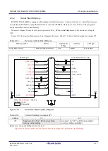
RTK7921053C00000BE is equipped with standard serial flash memory x 1 shown in Table 2.3.1. Serial flash memory
is controlled by RZ/A2M on-chip SPI multi-I/O bus controller (SPIBSC). During boot (boot mode 3), data (programs)
can be read from the serial flash memory.
Moreover, jumper JP1 may be set to provide power to PVcc_SPI and serial flash memory. Be sure to set voltage to
3.3V.
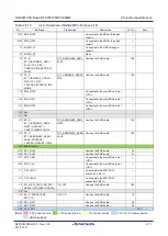
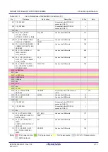
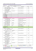
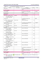
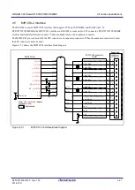
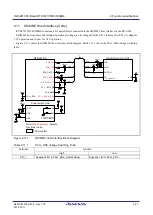
Figure 2.3.1 shows serial flash memory block diagram. Moreover, Table 2.3.2 shows function settings for jumper JP1.
Table 2.3.1
Overview of Serial Flash Memory
Memory Device
Model
Operational
Voltage
Capacity
Package
Serial flash memory
MX25L51245GXDI-08G
3.3V
64MB
24 ball BGA
Figure 2.3.1
Serial Flash Memory Block Diagram
Table 2.3.2
Function Settings for Jumper JP1
Jumper
1-2
2-3
JP1
Supplies 3.3 V to PVcc_SPI and serial flash
memory. (Initial setting)
Supplies 1.8 V to PVcc_SPI and serial flash
memory. (Setting prohibited)
[Note] shows the setting function to select.
If jumper JP1 is errorneously set, the memory may be damaged. Pay full attention to the setting.
RZ/A2M (U1)
QSPI0_SPCLK
14
D3_0
CLK_0
CS#_0
QSPI0_IO3
QSPI0_SSL
CLK_0
CS#_0
D3_0
RESET#
RPC_RESET#
RESET#
Serial Flash Memory (U2)
NC/SIO3
SCLK
CS#
RESET#
VCC
PVcc_SPI
ROMVcc
ROMVcc
ROMVcc
QSPI1_SPCLK
QSPI1_IO[3:0]
QSPI1_SSL
RPC_INT#
RPC_WP#
NC
NC
NC
NC
NC
Note:
Red characters
indicates
functions in use.
: Unmounted .
NC
NC
3.3V
1.8V
ROMVcc
1
3
JP1
CS#_1
D[3:0]_1
INT#
ROMVcc
ROMVcc
D[3:0]_1
CS#_1
INT#
CLK_1
CLK_1
D2_0
D2_0
WP#/SIO2
D[1:0]_0
D[1:0]_0
SO/SIO1, SI/SIO0
QSPI0_IO2
QSPI0_IO[1:0]
ROMVcc

