background image

29 


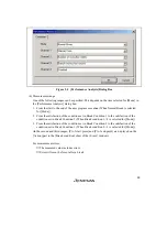
Figure 2.4   [Performance Analysis] Dialog Box 

(b) Measurement range 

One of the following ranges can be specified. This depends on the item selected for [Mode] in 
the [Performance Analysis] dialog box. 

1.  From the start to the end of the user program execution (When Normal Break is selected 

for [Mode]) 

2.  From the satisfaction of the condition set in Break Condition 1 to the satisfaction of the 

condition set in Break Condition 2 (When Break condition 1->2 is selected for [Mode]) 

3.  From the satisfaction of the condition set in Break Condition 2 to the satisfaction of the 

condition set in Break Condition 1 (When Break condition 2->1 is selected for [Mode]) 

(In the second and third ranges, [PA-1 start point] and [PA-1 end point] are displayed on the 
[Action] part in the [Break condition] sheet of the [Event] window.) 


For measurement errors, 


The measured value includes errors. 


Error will occur before or after a break. 


Summary of Contents for SuperH E10A

Page 1: ...Microcomputer Development Environment System SuperH Family SH7700 Series SH7710 E10A HS7710KCM02HE Rev 1 00 SuperHTM Family E10A Emulator Additional Document for User s Manual Specific Guide for the SH7710 E10A Emulator REJ10B0186 0100 ...

Page 2: ......

Page 3: ...efore making a final decision on the applicability of the information and products Renesas Technology Corp assumes no responsibility for any damage liability or other loss resulting from the information contained herein 5 Renesas Technology Corp semiconductors are not designed or manufactured for use in a device or system that is used under circumstances in which human life is potentially at stake...

Page 4: ......

Page 5: ...d Circuit 14 Pin Type 10 Section 2 Specifications of the SH7710 E10A Emulator s Software 13 2 1 Differences between the SH7710 and the Emulator 13 2 2 Specific Functions for the SH7710 E10A Emulator 17 2 2 1 Emulator Driver Selection 17 2 2 2 Break Condition Functions 18 2 2 3 Trace Functions 19 2 2 4 Notes on Using the JTAG Clock TCK and AUD Clock AUDCK 25 2 2 5 Notes on Setting the Breakpoint Di...

Page 6: ...ii ...

Page 7: ...nt System HITACHI PC Card PCMCIA or PCI 1 HS7710KCM01H PCMCIA 14 pin type Depth 85 6 mm Width 54 0 mm Height 5 0 mm Mass 27 0 g HS7710KCM02H PCMCIA 36 pin type Depth 85 6 mm Width 54 0 mm Height 5 0 mm Mass 28 0 g HS7710KCI01H PCI 14 pin type Depth 144 0 mm Width 105 0 mm Mass 93 0 g HS7710KCI02H PCI 36 pin type Depth 122 0 mm Width 96 0 mm Mass 90 0 g User system interface cable 1 HS7710KCM01H PC...

Page 8: ...KCM01SR HS0005KCM01HJ HS0005KCM01HE HS7710KCM02HJ and HS7710KCM02HE provided on a CD R Note The EMI is an abbreviation of the Electrical Magnetic Interference For EMI countermeasure use the ferrite core by connecting the user interface cable When the user interface cable is connected with the emulator or user system connect the ferrite core in the user system as shown in figure 1 1 User interface ...

Page 9: ...ction HS7710KCM02H HS7710KCI02H 36 pin connector Available HS7710KCM01H HS7710KCI01H 14 pin connector Not available The H UDI port connector has the 36 pin and 14 pin types as described below Use them according to the purpose of the usage 1 36 pin type with AUD function The AUD trace function is supported A large amount of trace information can be acquired in realtime The window trace function is ...

Page 10: ...anufacturing Ltd 14 pin straight type Note When designing the 36 pin connector layout on the user board do not connect any components under the H UDI connector When designing the 14 pin connector layout on the user board do not place any components within 3 mm of the H UDI port connector 1 4 Pin Assignments of the H UDI Port Connector Figures 1 2 and 1 3 show the pin assignments of the 36 pin and ...

Page 11: ...ESETP GND NC GND TRST GND TDI GND GND GND GND GND GND GND TDO ASEBRKAK User reset Output Output Output Input Input Input Input Output Output Output Output Output Output Output Output 1 2 3 4 5 6 7 8 9 10 11 12 13 14 15 16 17 18 19 20 21 22 23 24 25 26 27 28 29 30 31 32 33 34 35 36 Pin No Signal Input Output Note 1 1 2 5 2 4 2 3 SH7710 Pin No Pattern inhibited area Edge of the board connected to th...

Page 12: ... 2 54 15 24 2 54 0 45 Pin 1 Pin 8 Pin 7 Pin 14 Pin 1 mark H UDI port connector top view H UDI port connector top view Pin No Signal 1 2 3 4 5 6 7 8 9 11 10 12 and 13 14 TCK TRST TDO ASEBRKAK TMS TDI RESETP N C GND UVCC GND Input Output 1 2 2 2 GND 3 Output Input Input Output Output Input Input I O Output Note User reset 4 5 SH7710 Pin No 202 201 200 203 199 198 215 Unit mm Figure 1 3 Pin Assignmen...

Page 13: ...ct the signal lines to other components on the board 6 When the power of the emulator is turned on make sure that the emulator is inserted into the host computer and the power supply is turned on and the target system such as the system mounting the target device is connected to the emulator the power supply of the board is turned off the power supply voltage of the target device target system may...

Page 14: ... The result above differs depending on the circuit and can only be used as a reference 7 The resistance values shown in figure 1 5 are recommended 8 For the pin processing in cases where the emulator is not used refer to the hardware manual of the related device 9 For the AUDCK pin guard the pattern between the H UDI port connector and the MPU at GND level ...

Page 15: ...D GND GND GND GND GND GND GND GND GND GND 3 5 7 9 11 13 15 17 19 21 23 25 27 29 31 33 35 2 4 6 8 12 10 14 16 18 20 22 24 26 28 30 32 34 36 AUDCK N C 1 kΩ 4 7 kΩ AUDATA0 AUDATA2 AUDATA1 AUDATA3 TCK RESETP TMS TDO TDI TRST ASEBRKAK AUDCK AUDSYNC ASEMD0 AUDSYNC VccQ 3 3 V VccQ 3 3 V Figure 1 5 Recommended Circuit for Connection between the H UDI Port Connector and MPU 36 Pin Type ...

Page 16: ...s on the board 6 When the power of the emulator is turned on make sure that the emulator is inserted into the host computer and the power supply is turned on and the target system such as the system mounting the target device is connected to the emulator the power supply of the board is turned off the power supply voltage of the target device target system may become higher around 1 2 V to 1 4 V t...

Page 17: ...n figure 1 7 are recommended 8 For the pin processing in cases where the emulator is not used refer to the hardware manual of the related device 1 TCK TMS N C TDO TDI GND GND GND GND GND GND 2 3 4 5 6 7 8 9 11 10 12 13 14 H UDI port connector 14 pin type SH7710 Reset signal 4 7 kΩ RESET 1 kΩ 4 7 kΩ ASEBRKAK TRST TCK RESETP TMS TDO TDI TRST ASEBRKAK ASEMD0 VccQ 3 3 V VccQ 3 3 V Figure 1 7 Recommend...

Page 18: ...12 ...

Page 19: ...rs are undefined Table 2 1 Register Initial Values at Emulator Link Up Register Emulator at Link Up R0 to R14 H 00000000 R15 SP H A0000000 R0_BANK to R7_BANK H 00000000 PC H A0000000 SR H 700000F0 GBR H 00000000 VBR H 00000000 MACH H 00000000 MACL H 00000000 PR H 00000000 SPC H 00000000 SSR H 000000F0 RS H 00000000 RE H 00000000 MOD H 00000000 A0G A1G H 00000000 A0 A1 H 00000000 X0 X1 H 00000000 Y...

Page 20: ... memory access 5 Direct Memory Access Controller DMAC The DMAC operates even when the emulator is used When a data transfer request is generated the DMAC executes DMA transfer 6 Memory Access during User Program Execution When a memory is accessed from the memory window etc during user program execution the user program is resumed after it has stopped in the E10A emulator to access the memory Ther...

Page 21: ...ogram jumps to the user exception handler in TLB Mode in the Configuration dialog box When TLB miss exception is enable is selected a Communication Timeout error will occur if the TLB exception handler does not operate correctly When TLB miss exception is disable is selected the program does not jump to the TLB exception handler even if a TLB exception occurs Therefore if the TLB exception handler...

Page 22: ...ng the SDMR register specify addresses to be accessed in the I O register definition file SH7710 IO and then activate the HEW After the I O register file is created the MPU s specification may be changed If each I O register in the I O register definition file differs from addresses described in the hardware manual change the I O register definition file according to the description in the hardwar...

Page 23: ...ection Table 2 3 shows drivers which are selected in the E10A Driver Details dialog box Table 2 3 Type Number and Driver Type Number Driver HS7710KCM01H E10A PC Card Driver 3 HS7710KCM02H E10A PC Card Driver 4 HS7710KCI01H E10A PCI Card Driver 3 HS7710KCI02H E10A PCI Card Driver 4 ...

Page 24: ...d Write condition Breaks when the SH7710 RD or RDWR signal level matches the specified condition Bus state condition Breaks when the operating state in an SH7710 bus cycle matches the specified condition Types of buses that can be specified are listed below L bus CPU ALL Indicates an instruction fetch and data access including a hit to the cache memory L bus CPU Data Indicates a data access by the...

Page 25: ...X X X O O Notes 1 O Can be set in the dialog box X Cannot be set in the dialog box 2 For Break Condition 2 X bus and Y bus conditions cannot be specified 2 2 3 Trace Functions The SH7710 E10A emulator supports the trace functions listed in table 2 6 Table 2 6 Trace Functions Function Internal Trace AUD Trace Branch trace Supported eight branches Supported Range memory access trace Not supported Su...

Page 26: ... output is output but the next trace information is not output The user program can be executed in realtime but some trace information may be lost Non realtime trace When the next branch occurs while the trace information is being output the CPU stops operations until the information is output The user program is not executed in realtime Trace buffer full Trace continue This function overwrites th...

Page 27: ...menu to display the Acquisition dialog box The AUD trace acquisition mode can be set in the AUD mode1 or AUD mode2 group box in the Trace mode page of the Acquisition dialog box Figure 2 1 Trace mode Page When the AUD trace function is used select the AUD function radio button in the Trace type group box of the Trace mode page ...

Page 28: ... Branch trace Page b Window Trace Function Memory access in the specified range can be acquired by trace Two memory ranges can be specified for channels A and B The read write or read write cycle can be selected as the bus cycle for trace acquisition Setting Method i Select the Channel A and Channel B check boxes in the AUD function group box of the Trace mode page Each channel will become valid i...

Page 29: ...he address information acquired by the I bus is 28 bits and the upper 4 bits are displayed as The source cannot be displayed in the Trace window When U RAM or X Y RAM is accessed from the P0 space the I bus must be selected and when accessed from the P2 space the L bus must be selected When a cache fill cycle is acquired I bus must be selected 2 Address setting when X Y bus is selected To trace bo...

Page 30: ...sses If the previous branch source address is the same as the upper 16 bits the lower 16 bits are output If it matches the upper 24 bits the lower 8 bits are output If it matches the upper 28 bits the lower 4 bits are output The emulator regenerates the 32 bit address from these differences and displays it in the Trace window If the emulator cannot display the 32 bit address it displays the differ...

Page 31: ...Trace information cannot be acquired for the following branch instructions The BF and BT instructions whose displacement value is 0 Branch to H A0000000 by reset 4 The internal trace acquisition is not available when User is selected in the UBC mode list box of the Configuration dialog box In this case close the Trace window 2 2 4 Notes on Using the JTAG Clock TCK and AUD Clock AUDCK 1 Set the JTA...

Page 32: ...P_SET command setting is disabled The ASID value of the SH7710 PTEH register during command input is used When VPMAP_SET command setting is enabled a BREAKPOINT is set to a physical address into which address translation is made according to the VP_MAP table However for addresses out of the range of the VP_MAP table the address to which a BREAKPOINT is set depends on the SH7710 MMU status during c...

Page 33: ...isabled when an instruction to which a BREAKPOINT has been set is executed Accordingly do not set a BREAKPOINT to an instruction which satisfies Break Condition 2 3 When a Break Condition is satisfied emulation may stop after two or more instructions have been executed 4 If a PC break address condition is set to the slot instruction after a delayed branch instruction user program execution cannot ...

Page 34: ...alog box is displayed by selecting Setting Note For the command line syntax refer to the online help a Specifying the measurement start end conditions The measurement start end conditions are specified in the Mode drop down list box in the Performance Analysis dialog box Three conditions can be set as shown in table 2 9 Table 2 9 Conditions Specified in Mode Item Description Normal break Measureme...

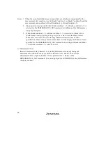
Page 35: ...k Condition 1 to the satisfaction of the condition set in Break Condition 2 When Break condition 1 2 is selected for Mode 3 From the satisfaction of the condition set in Break Condition 2 to the satisfaction of the condition set in Break Condition 1 When Break condition 2 1 is selected for Mode In the second and third ranges PA 1 start point and PA 1 end point are displayed on the Action part in t...

Page 36: ...e of the Performance Analysis dialog box specify one or more items for measurement When there is no item the error message Measurement item does not have specification Please set up a measurement item will be displayed When no item is specified for the PERFORMANCE_SET command the settings of Break condition 1 2 or Break condition 2 1 will be an error c Measurement item Items are measured with Chan...

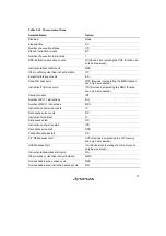
Page 37: ...LB miss cycle ITS Devices incorporating the MMU function can only be measured Interrupt counts INT Number of BL 1 instructions BL1 Number of MD 1 instructions MD1 Instruction cache miss counts IC Data cache miss counts DC Instruction fetch stall IF Data access stall DA Instruction cache miss stall ICS Data cache miss stall DCS Cacheable access stall CS X Y RAM access stall XYS Devices incorporatin...

Page 38: ...on Notes No caching due to the settings of TLB cacheable bit Counted for accessing the cacheable area Cache on counting Accessing the non cacheable area is counted less than the actual number of cycles and counts Accessing the cacheable X Y RAM and U RAM areas is counted more than the actual number of cycles and counts Branch count The counter value is incremented by 2 This means that two cycles a...

Page 39: ...s as a result of measurement will be displayed 3 Initializing the measured result To initialize the measured result select Initialize from the popup menu in the Performance Analysis window or specify INIT with the PERFORMANCE_ANALYSIS command ...

Page 40: ...34 ...

Page 41: ...he SH7710 E10A Emulator Publication Date Rev 1 00 March 1 2005 Published by Sales Strategic Planning Div Renesas Technology Corp Edited by Technical Documentation Information Department Renesas Kodaira Semiconductor Co Ltd 2005 Renesas Technology Corp All rights reserved Printed in Japan ...

Page 42: ... Fax 44 1628 585 900 Renesas Technology Hong Kong Ltd 7th Floor North Tower World Finance Centre Harbour City 1 Canton Road Tsimshatsui Kowloon Hong Kong Tel 852 2265 6688 Fax 852 2730 6071 Renesas Technology Taiwan Co Ltd 10th Floor No 99 Fushing North Road Taipei Taiwan Tel 886 2 2715 2888 Fax 886 2 2713 2999 Renesas Technology Shanghai Co Ltd Unit2607 Ruijing Building No 205 Maoming Road S Shan...

Page 43: ...SuperH Family E10A Emulator Additional Document for User s Manual Specific Guide for the SH7710 E10A Emulator ...

Reviews: