background image


RF-BM-S02 

www.szrfstar.com

                                                                                                                                                    V1.0 - May, 2020 

Shenzhen RF-star Technology Co., Ltd.                                                                                                                   

Page  11  of  23


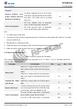
Tolerance

5


Spurious  Emission.  Only 

Largest  Spurious  Emission 

Stated within Each Band. 

Conducted  measurement  with  a  50-Ω  single-

ended load. Complies with EN 300 328, EN 300 

440  class  2,  FCC  CFR47,  Part  15  and ARIB 

STD-T-66 


-75 


dBm 

Current Consumption 

RX  mode,  standard  mode,  no  peripherals 

active, low MCU activity, MCU at 250 kHz 


19.6 


mA 

RX  mode,  high-gain  mode,  no  peripherals 

active, low MCU activity, MCU at 250 kHz 


22.1 


mA 

Note:   

1. 

0.1% BER maps to 30.8% PER. 

2. 

The receiver sensitivity setting is programmable using a TI BLE stack vendor-specific API command. The default 

value is standard mode. 

3. 

Results based on standard gain mode. 

4. 

Difference between center frequency of the received RF signal and local oscillator frequency. 

5. 

Difference between incoming symbol rate and the internally generated symbol rate. 

3.4 Transceiver RF Parameters   

Table 6. Table of Transceiver RF Parameters 

When measured on the RF-BM-S02 reference design with T A = 25 

, V BAT = 3.3 V, Fc = 2440 MHz with DC/DC 

enabled unless otherwise noted. 

Parameters 

Test Condition 

Min. 

Typ. 

Max. 

Unit 

Output Power 

Delivered  to  a  single-ended  50-Ω  load  through  a 

balun using maximum recommended output power 

setting 


dBm 

Delivered  to  a  single-ended  50-Ω  load  through  a 

balun using minimum recommended output power 

setting 


-23 


dBm 

Programmable  Output 

Power Range 

Delivered  to  a  single-ended  50  Ω  load  through  a 

balun 


27 


dB 

Spurious Emissions 

Conducted measurement with a 50-Ω single-ended 

load. Complies with EN 300 328, EN 300 440 class 

2, FCC CFR47, Part 15 and ARIB STD-T-66 


-41 


dBm 

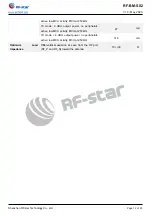
Current Consumption 

TX  mode,  -23  dBm  output  power,  no  peripherals 

active, low MCU activity, MCU at 250 kHz 


21.1 


mA 

TX  mode,  -6  dBm  output  power,  no  peripherals 


23.8 


mA 

Summary of Contents for RF-BM-S02

Page 1: ...RF BM S02 Bluetooth Low Energy Module Version 1 0 Shenzhen RF star Technology Co Ltd May 15th 2020...

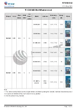
Page 2: ...B 13 7 17 4 100 RF BM S02 PCB 11 2 15 2 100 RF BM S02I IPEX 11 2 15 2 150 RF CC2540A1 PCB 15 2 24 1 100 CC2541 8051 256 8 0 RF BM S01A PCB 13 7 17 4 70 RF BM S02A PCB 11 2 15 2 70 RF BMPA 2541B1 PCB I...

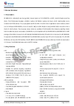
Page 3: ...um output power in TX mode The RF BM S02A also adds a HW I2 C interface 1 2 Key Features RF Bluetooth low energy 4 0 compatible protocol stack for single mode Excellent link budget up to 97 dBm Enabli...

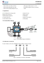
Page 4: ...tronics Human interface devices Keyboard mouse Remote control USB dongles Health care and medical Smart lighting 1 4 Functional Block Diagram Figure 1 Functional Block Diagram of RF BM S02 1 5 Part Nu...

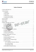
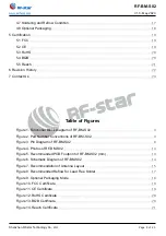
Page 5: ...unctions 7 2 1 Module Parameters 7 2 2 Module Pin Diagram 8 2 3 Pin Functions 8 3 Specifications 10 3 1 Recommended Operating Conditions 10 3 2 Handling Ratings 10 3 3 Receiver RF Parameters 10 3 4 Tr...

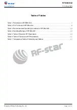
Page 6: ...gram of RF BM S02 3 Figure 2 Part Number Conventions of RF BM S02 3 Figure 3 Pin Diagram of RF BM S02 8 Figure 4 Photos of RF BM S02 13 Figure 5 Recommended PCB Footprint of RF BM S02 mm 13 Figure 6 S...

Page 7: ...le 1 Parameters of RF BM S02 7 Table 2 Pin Functions of RF BM S02 8 Table 3 Recommended Operating Conditions of RF BM S02 10 Table 4 Handling Ratings of RF BM S01 10 Table 5 Table of Receiver RF Param...

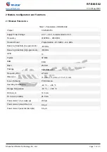
Page 8: ...it Power Programmable 23 0 dBm 4 0 dBm Receiving Sensitivity low gain mode 87 dBm Receiving Sensitivity high gain mode 93 dBm GPIO 13 Crystal 32 MHz RAM 8 KB Flash 256 KB Package SMT Packaging Frequen...

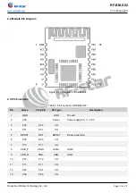
Page 9: ...2 3 Pin Functions Table 2 Pin Functions of RF BM S02 Pin Name Chip Pin Pin Type Description 1 GND GND Ground 2 VCC Power Power supply 2 0 V 3 6 V 3 P22 P2 2 I O 4 P21 P2 1 I O 5 RESET RST RESET Reset...

Page 10: ...RF BM S02 www szrfstar com V1 0 May 2020 Shenzhen RF star Technology Co Ltd Page 9 of 23 14 P05 P0 5 I O 15 P04 P0 4 I O 16 P03 P0 3 I O 17 P02 P0 2 I O 18 P01 P0 1 I O...

Page 11: ...of RF BM S01 Items Condition Min Typ Max Unit Storage Temperature Tstg 40 25 125 Human Body Model HBM 2000 V Moisture Sensitivity Level 2 Charged Device Model 750 V 3 3 Receiver RF Parameters Table 5...

Page 12: ...l oscillator frequency 5 Difference between incoming symbol rate and the internally generated symbol rate 3 4 Transceiver RF Parameters Table 6 Table of Transceiver RF Parameters When measured on the...

Page 13: ...ivity MCU at 250 kHz TX mode 0 dBm output power no peripherals active low MCU activity MCU at 250 kHz 27 mA TX mode 4 dBm output power no peripherals active low MCU activity MCU at 250 kHz 31 6 mA Opt...

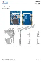
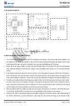
Page 14: ...0 May 2020 Shenzhen RF star Technology Co Ltd Page 13 of 23 4 Application Implementation and Layout 4 1 Module Photos Figure 4 Photos of RF BM S02 4 2 Recommended PCB Footprint Figure 5 Recommended P...

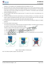
Page 15: ...to the long term stable operation of the whole machine The module should be far away from the power electromagnetic transformer high frequency wiring and other parts with large electromagnetic interfe...

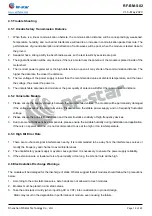
Page 16: ...nd preferably vertically upward When the module is installed inside of the case a high quality antenna extension wire can be used to extend the antenna to the outside of the case 10 The antenna must n...

Page 17: ...tage is between the recommended values The module will be permanently damaged if the voltage exceeds the maximum value Please ensure the stable power supply and no frequently fluctuated voltage 2 Plea...

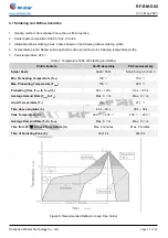
Page 18: ...245 Table 7 Temperature Table of Soldering and Reflow Profile Feature Sn Pb Assembly Pb Free Assembly Solder Paste Sn63 Pb37 Sn96 5 Ag3 0 Cu0 5 Min Preheating Temperature Tmin 100 150 Max Preheating...

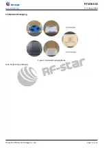
Page 19: ...RF BM S02 www szrfstar com V1 0 May 2020 Shenzhen RF star Technology Co Ltd Page 18 of 23 4 8 Optional Packaging Figure 9 Optional Packaging Mode Note Default tray packaging...

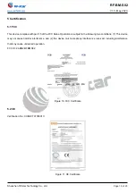
Page 20: ...5 of the FCC Rules Operation is subject to the following two conditions 1 This device may not cause harmful interference and 2 this device must accept any interference received including interference...

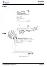
Page 21: ...02 www szrfstar com V1 0 May 2020 Shenzhen RF star Technology Co Ltd Page 20 of 23 5 3 RoHS Report No DTI201801253515 Figure 12 RoHS Certificate 5 4 BQB Qualified Design ID B016552 Figure 13 BQB Certi...

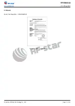
Page 22: ...RF BM S02 www szrfstar com V1 0 May 2020 Shenzhen RF star Technology Co Ltd Page 21 of 23 5 5 Reach Reach Test Report No C150918025001 Figure 14 Reach Certificate...

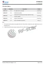
Page 23: ...oo Wang 2018 02 26 V1 0 Update module operating and storage temperature range Add CE certificate Aroo Wang 2018 08 02 V1 0 Update company address Aroo Wang 2020 05 15 V1 0 Add TI CC254X BLE module lis...

Page 24: ...Y CO LTD Shenzhen HQ Add Room 601 Block C Skyworth Building High tech Park Nanshan District Shenzhen Guangdong China Tel 86 755 3695 3756 Chengdu Branch Add No B3 03 Building No 1 Incubation Park High...

Reviews: