RFD900ux Data Sheet
www.rfdesign.com.au
14
Last update 12/09/2019
10
PCB Design Guidelines
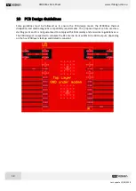
Some guidelines must be followed as to ensure the PCB design meets the RFD900ux thermal
dissipation and electromagnetic compatibility requirements. The proposed layout can be used as a
starting point and it is not guaranteed to comply with EM immunity and emissions regulations as is.
The PCB designer is expected to calculate the RF antenna track widths to be 50
Ω
outputs, depending
on the host PCB layer stack up and dielectric constant.


