RFL 9508 PLC-TT
RFL Electronics Inc.
September 5, 2012
13
(973) 334-3100
MISCELLANEOUS CIRCUITS
The transfer trip module has eight LEDs on the front to indicate the condition of the trip inputs and
outputs. These LEDs are driven by a latch which is memory mapped off the processor. An additional
LED indicates an alarm condition. This LED and a local alarm relay are directly driven by the
processor. A five position DIP switch is provided to allow the user to set the SCB address of the
module. The processor reads the switch to setup the SCB FPGA.
I/O ADAPTER MODULE(S)
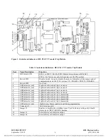
The transfer trip module must be used with one of eight I/O Adapter Modules. There are two and four
function versions, and relay and solid state versions. See Figures 2 and 3, and Table 2. The two
function version is assembled from two PCBs; one for inputs and alarms, and the other for outputs. The
four function version uses the same two boards as the two function version but has an additional input
and output board. The boards are interconnected via a series of short cables.
INPUT BOARD
The input board contains circuitry for two optically isolated inputs and one form C alarm relay. The
components consist mainly of dropping resistors, a zener diode, and an optoisolator. An LC filter is
also provided to prevent SWC from triggering an input. The dropping resistors are sized to allow a safe
level of current to be drawn from the keying input. The zener diode and resistors prevent any voltage
less than half the nominal keying voltage from causing an input. The optoisolator provides galvanic
isolation from the keying circuits.
OUTPUT BOARD
The output board can be configured for either solid state or relay outputs. Each output board provides
two outputs. The solid state output takes the oscillating trip signal and feeds it across a transformer to
isolate it and then rectifies and smoothes the result. This feeds the gate of a FET transistor. The
transistor is rated to carry many times the rated load for short periods but thermal limitations prevent it
from carrying a large load indefinitely. An LC filter protects the FET from damage caused by surges on
the outputs. The relay version of the output board has two output relays with LC filters. The relays
have diodes to prevent the flyback effect from creating spurious noise.
DIRECTIONAL COMPARISON BLOCKING MODE
All PLC-TT modules are capable of being used in directional comparison blocking applications. The
functionality of the PLC-TT is transformed into that of a typical single function carrier system. Inputs
one and two are used as start and stop inputs. Outputs one and two are block outputs. Functions three
and four remain normal transfer trip functions. Figure 6 illustrates how the unit works.
Software settable jumpers J1 and J2 allow for optional inversion of the start and stop inputs. They are
controlled by the settings described below. The start input will cause function 1 trip to be sent if the
stop input is not active. When Function 1 is sent, the block outputs (outputs 1 and 2) are made active. If
Function 1 is received the outputs go active as well.


