background image

SERVICE NOTES

Issued by RJA

Copyright © 2008 Roland Corporation

All rights reserved. No part of this publication may be reproduced in any form without the written permission 
of Roland Cororation.

Printed in Japan (0290) (CC-KWS)

17058541E0

Mar. 2008

GT-10

Preliminar

y

Table of Contents

Cautionary Notes ..............................................................2
Main Specifications ...........................................................3
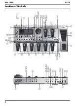
Location of Controls .........................................................4
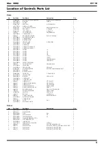
Location of Controls Parts List........................................5
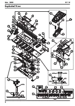
Exploded View ..................................................................6
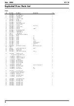
Exploded View Parts List.................................................8
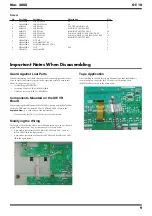
Important Notes When Disassembling..........................9
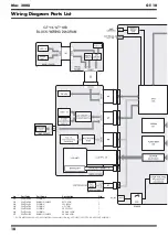
Wiring Diagram Parts List .............................................10
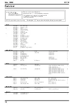
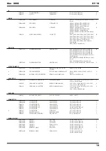
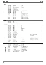
Parts List ...........................................................................12
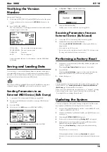
Verifying the Version Number......................................15
Saving and Loading Data...............................................15
Performing a Factory Reset............................................15
Updating the System ......................................................15
Test Mode .........................................................................16

Circuit Board (Main Board) ...........................................24
Circuit Diagram (Main Board: 1/5) ..............................26
Circuit Diagram (Main Board: 2/5) ..............................28
Circuit Diagram (Main Board: 3/5) ..............................30
Circuit Diagram (Main Board: 4/5) ..............................32
Circuit Diagram (Main Board: 5/5) ..............................34
Circuit Board (SW VR, Pedal, Bank, ENC, 
EXP Board) .......................................................................36
Circuit Diagram (SW VR Board) ...................................38
Circuit Diagram (Pedal Board)......................................40
Circuit Diagram (Bank Board).......................................42
Circuit Diagram (ENC Board) .......................................42
Circuit Diagram (EXP Board) ........................................43
Determination of Main Board Model ...........................43

Summary of Contents for Boss GT-10

Page 1: ...Notes When Disassembling 9 Wiring Diagram Parts List 10 Parts List 12 Verifying the Version Number 15 Saving and Loading Data 15 Performing a Factory Reset 15 Updating the System 15 Test Mode 16 Circu...

Page 2: ...7327R0 Insulating Washer 14 5X9 2 G2637118R0 USB Connector Cap USBC 1 05015034 Parts List A component whose part code is cannot be supplied as a service part because one of the following reasons appli...

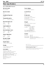
Page 3: ...T jack coaxial type MIDI connectors IN OUT DC IN jack Power Supply DC 9 V AC Adaptor Roland PSB 1U Current Draw 800 mA Dimensions 542 W x 272 D x 77 H mm 21 3 8 W x 10 3 4 D x 3 1 16 H inches Maximum...

Page 4: ...4 Mar 2008 GT 10 Location of Controls fig panel GT 10 eps...

Page 5: ...LED SPACER LEDS 10 5 8 32 F3229187R0 POTENTIOMETER RV112FF 40B1 15F 0B20K 0057 4 33 G2477525R0 R KNOB 4 34 G2497021R0 KEYTOP UNIT S 1 35 F5229819R0 LED RED L 7104SURC E 10 36 G2147913R0 LED SPACER 2 3...

Page 6: ...6 Mar 2008 GT 10 Exploded View fig bunkai eps L...

Page 7: ...7 Mar 2008 GT 10 fig bunkai eps R...

Page 8: ...357120R0 FOOT H 5 5 41 F5229821R0 LCD UNIT W WIRING KMC13264 H 00 SPF 1 42 12499175 1 43 05015034 USB CONNECTOR CAP USBC 1 1 44 G2147913R0 LED SPACER 2 45 G2257327R0 JACK BUSH 1 46 G2637118R0 INSULATI...

Page 9: ...too long modify the cable as shown below 3 pin ribbon cable between SW VR Board CN105 and ENC encoder Board CN501 A in the figure below 9 pin ribbon cable between Pedal Board CN202 and Bank Board CN30...

Page 10: ...ing LCD UNIT LCD FPC BACKLIGHT WIRING No Part Code Part Name Description Q ty W1 F3417194R0 WIRING EXP 3PIN 1 W2 F3417195R0 RIBBON CABLE ENC 3PIN 1 W3 F3417196R0 WIRING SW 12PIN 1 W4 F3417197R0 WIRING...

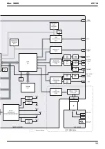
Page 11: ...11 Mar 2008 GT 10 fig block wiring eps R...

Page 12: ...BER SW ESCUTCHEON 1 KNOB BUTTON G2477526R0 R KNOB INDEX OUTPUT LEVEL Knob 1 G2497019R0 KEYTOP CLEAR 5H SW VR Board 2 G2477528R0 CURSOR KEY A SW VR Board 1 G2477527R0 CURSOR KEY B SW VR Board 1 G247752...

Page 13: ...15F 0B20K 0057 VR102 VR103 VR104 VR105 on SW VR Board 4 F3229203R0 ROTARY POTENTIOMETER RD901F 40 15F B10K 0068 VR101 on SW VR Board 1 CAPACITOR F3639959R0 CHEMICAL CAPACITOR SVP220M1CD05M C109 C112 C...

Page 14: ...794R0 LABEL CTL 1 1 G2217791R0 LABEL CTL 2 1 05015034 USB CONNECTOR CAP USBC 1 1 22365714 CORD HOOK 1 G2237632R0 GUARD PLATE 1 G2207422R0 GUARD ESCT 1 G2257331R0 INSULATING SHEET 1 G2257332R0 JACK COV...

Page 15: ...2 Send bulk data from the external MIDI device The message BULK DATA RECEIVING is displayed while data is being received No operation on the GT 10 is needed If data is not received verify that the de...

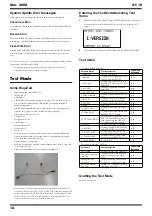
Page 16: ...the settings file and the like The GT 10 USB Driver and USBCheck exe are obtained via Service Network USBCheck exe runs only under Windows XP Entering the Test Mode Selecting Test Items 1 Hold down O...

Page 17: ...test Descriptions of Errors PR Check of DSP IC3 internal program RAM An error indicates either an internal defect in the DSP IC3 or a defective bus connection with the CPU IC2 DT Check of DSP IC3 int...

Page 18: ...the next test 6 PARAM KNOB Testing of the PARAMETER Controls fig 6paramknob2 eps 1 Turn the PARAMETER 1 control clockwise by 360 degrees or more 2 Verify that the these values are displayed 1 4 2 4 3...

Page 19: ...xt test 9 MIDI MIDI Test fig 9midi2 eps When no MIDI cable is connected the message No Connection is displayed 1 Connect the MIDI IN and MIDI OUT jacks using a MIDI cable 2 When the message Pull out t...

Page 20: ...o the left channel and right channel monitor speakers 2 Verify that the INSERT PHONES message disappears from the screen 3 Verify that the output waveform display on the oscilloscope is what is shown...

Page 21: ...at the peak value for both the left and right channels is 1 55 to 1 75 V substantially the same as before the plug was unplugged from the PHONES jack 5 Verify that signals are output from the monitor...

Page 22: ...t the OUTPUT L and R jacks to the left and right channel monitor speakers 7 Press the WRITE button and verify that the Check INPUT Noise message displayed changes to Check SHOCK Noise 8 Verify that th...

Page 23: ...akers 2 Connect headphones to the PHONES jack 3 Verify that no abnormal noise is heard from the monitor speakers or headphones at the moment the power is switched on 4 Verify that the unit starts up i...

Page 24: ...24 Mar 2008 GT 10 Circuit Board Main Board fig b main 1 eps...

Page 25: ...25 Mar 2008 GT 10 fig b main 2 eps...

Page 26: ...26 Mar 2008 GT 10 Circuit Diagram Main Board 1 5 fig d main 1 eps L...

Page 27: ...27 Mar 2008 GT 10 fig d main 1 eps R...

Page 28: ...28 Mar 2008 GT 10 Circuit Diagram Main Board 2 5 fig d main 2 eps L...

Page 29: ...29 Mar 2008 GT 10 fig d main 2 eps R...

Page 30: ...30 Mar 2008 GT 10 Circuit Diagram Main Board 3 5 fig d main 3 e eps L...

Page 31: ...r 2008 GT 10 fig d main 3 e eps R The value of resistor R252 varies according to the production period The respective serial numbers are indicated below ZW78199 or earlier 10 ohms ZW88200 or later 47...

Page 32: ...32 Mar 2008 GT 10 Circuit Diagram Main Board 4 5 fig d main 4 eps L...

Page 33: ...33 Mar 2008 GT 10 fig d main 4 eps R...

Page 34: ...34 Mar 2008 GT 10 Circuit Diagram Main Board 5 5 fig d main 5 eps L...

Page 35: ...35 Mar 2008 GT 10 fig d main 5 eps R...

Page 36: ...36 Mar 2008 GT 10 Circuit Board SW VR Pedal Bank ENC EXP Board fig b sw 1 eps...

Page 37: ...37 Mar 2008 GT 10 fig b sw 2 eps...

Page 38: ...38 Mar 2008 GT 10 Circuit Diagram SW VR Board fig d sw vr eps L...

Page 39: ...39 Mar 2008 GT 10 fig d sw vr eps R...

Page 40: ...40 Mar 2008 GT 10 Circuit Diagram Pedal Board fig d pedal eps L...

Page 41: ...41 Mar 2008 GT 10 fig d pedal eps R...

Page 42: ...42 Mar 2008 GT 10 Circuit Diagram Bank Board fig d bank eps Circuit Diagram ENC Board fig d enc eps...

Page 43: ...tion of Main Board Model The Main Board Assy for both the GT 10 and the GT 10B uses the same bare circuit board but the mounted components are different To distinguish between the two examine the mode...

Page 44: ...MEMO Mar 2008 GT 10...

Reviews: