2A3/4
2-3-2
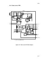
The power source PCB (PSPCB) is a switching regulator which converts an AC input to
generate 24 V DC, 5.1 V DC and 12 V DC. It consists of the components shown in
Figure 2-3-1; noise filter circuit, rectifier circuit, switching control circuit, 24 V DC output
circuit, 5.1 V DC output circuit, 12 V DC output circuit, fixing heater control circuit,
overvoltage detection circuit, overcurrent detection circuit.
The noise filter circuits, consisting mainly of the noise filter circuit in the power source
section and capacitors, attenuates external noise and prevents switching noise
generated by the power source circuit and the heater control circuit from leaving the
machine via the AC line.
The rectifier circuit full-wave rectifies the AC input which has passed through the noise
filter circuit using the diode bridge D001.
The switching control circuit turns the FETs Q1 and Q2 on and off via the PWM
controller IC1 to apply the AC component from the DC voltage smoothed via the
electrolytic capacitor C101 to the primary coil of the transformer TRNS.
The 24 V DC output circuit smoothes the current induced on the secondary coil of the
transformer TRNS via diodes D201 and D202, and outputs a more stable 24 V DC by
the function of shunt regulator IC2. The output status of 24 V DC is fed back to the
PWM control IC1 in the switching control circuit via the photocoupler PC1, and based on
the feedback, the PWM control IC1 outputs stable 24 V DC constantly by controlling the
switching duty pulse width for the FETs Q1 and Q2.
The 5.1 V DC output control circuit IC3 receive 24 V DC from the 24 V DC output circuit
and output stable 5.1 V DC by the function of the DC/DC converter control IC3.
The 12 V DC output circuit receive 24 V DC from the 24 V DC output circuit and outputs
stable 12 V DC by the function of a power supply regulator.
In the energy saving mode, the FETs Q210 and Q302 are opened when they receive a
sleep signal from the main PCB (MPCB), thus cutting off the output of 24 V DC and a
part of 5.1 V DC. Since input to the 12 V DC control circuit IC4 is also cut off, output of
12 V DC also ceases.
As a result, all outputs except the sub-output from the 5.1 V DC output circuit IC3 are
cut off, by which means energy consumption is lowered to the Energy Star accreditation
level while in the stand-by mode.
Abnormal rise of voltage for all DC outputs and overcurrent in all outputs except the 24
V DC and 12 V DC outputs are monitored by the overvoltage and overcurrent detection
circuits, and if any abnormal rise is detected, alarm signals are fed back to the PWM
control circuit IC1 on the primary side via photocoupler PC2, by which means power
supply is shut down. Overload of the 24 V DC output is monitored by resistor R129 as
the total sum of current on the primary side, and if any abnormal condition is detected,
the operation of the PWM control circuit IC1 stops and the power supply is shut down.
Overload of the 12 V DC output circuit is controlled by the overcurrent protection
function of power source regulator IC4. When the abnormal output condition is
removed, the 12 V DC output returns to the normal output condition.
The fixing heater control circuit sends zero-crossing signal (Z CROSS SIG) via the
photocoupler PC3 to the main PCB (MPCB). These signals are in turn converted into
signals to control the on/off timing and phases, which are then input to the power source
PCB (PSPCB) as the H1 REM and H2 REM signals. The phototriacs PT1 and PT2 are
turned on by the H1 REM and H2 REM signals, and electricity flows through triacs TR2
and TR3 to turn the fixing heaters on.
Summary of Contents for Ri 4230
Page 3: ...SERVICE MANUAL Ri 4230 5230 ...
Page 13: ...4230 5230 S M MCA THEORY AND CONSTRUCTION SECTION I I Theory and Construction Section ...
Page 14: ...1 1 5 2A3 4 CONTENTS 1 1 Specifications 1 1 1 Specifications 1 1 1 ...
Page 100: ...4230 5230 S M MCA ELECTRICAL SECTION II II Electrical Section ...
Page 119: ......
Page 138: ......
Page 159: ...4230 5230 S M MCA III Set Up and Adjustment Section III SET UP AND ADJUSTMENT SECTION ...
Page 448: ...2A3 4 3 6 3 25 Toner scatters at the leading edge of the image See page 3 6 17 ...


