background image

84

CMX32M cpuModule

BDM-610000075

Rev B


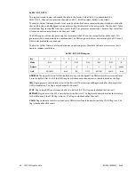
Multi-Color LED

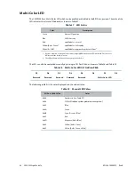
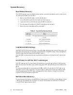
The CMX32M has a Multi-Color LED which can be enabled or disabled in the BIOS setup screen. The color of the 
LED indicates the status of the board, as shown in Table 57.

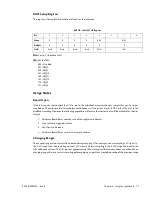
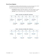
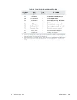
The LED can also be controlled manually by writing to I/O Port 984h, as shown in Table 58 and Table 59

The following table lists the color displayed and the value written.

Table 57

LED Colors

Color

Description

Green

Normal Operation

Blue

SATA Activity

Red

cpuModule is in reset

1

1. If power is applied to the cpuModule while jumper 

JP5

 is installed, the LED will be red. This does not 

indicate that the board is in reset

Yellow (Red + Green)

cpuModule is in Standby

White (R+G+B)

cpuModule is approaching thermal limit

2

2. The LED will remain White until the system is shut down.

Table 58

Multi-Color LED I/O Address 984h

D7

D6

D5

D4

D3

D2

D1

D0

Reserved Reserved Reserved Reserved

Reserved

Multi-Color 

LED

Table 59

Manual LED Colors

I/O Port 984h Value

Color

0x00

Automatic (see Table 57)

0x08

Off (

will reduce system power consumption.)

0x09

Blue

0x0A

Green

0x0B

Cyan (Green + Blue)

0x0C

Red

0x0D

Magenta (Red + Blue)

0x0E

Yellow (Red + Green)

0x0F

White (Red + Green + Blue)

Summary of Contents for BDM-610000075

Page 1: ...ISO9001 and AS9100 Certified Accessing the Analog World www rtd com CMX32M cpuModules User s Manual BDM 610000075 Revision B ...

Page 2: ...PCI 104 Express and 104 are trademarks of the PC 104 Embedded Consortium All other trademarks appearing in this doc ument are the property of their respective owners Failure to follow the instructions found in this manual may result in damage to the product described in this manual or other components of thesystem The procedure set forth in this manual shall only be performed by persons qualified ...

Page 3: ... Accessing the Analog World www rtd com ISO9001 and AS9100 Certified CMX32M cpuModules ...

Page 4: ...iv CMX32M cpuModule BDM 610000075 Rev B ...

Page 5: ...11 Operating Conditions 11 Electrical Characteristics 12 Contact Information 14 Chapter 2 Getting Started Connector Locations 16 Selecting the Stack Order for the CMX32M 18 Stack Example 19 Connecting to the Stack 20 Connecting the Utility Cable 21 Connecting a Keyboard 21 Booting the CMX32M cpuModule for the First Time 21 Chapter 3 Connecting the cpuModule Proper Grounding Techniques 24 Connector...

Page 6: ...N1 Top 43 PCIe 104 Type 2 Compatibility 45 PCIe Link Configuration 46 PCIe Peer To Peer 46 PCIe 104 Type 1 Bus CN2 Bottom 47 PCI 104 Express PCIe Bus Signals 49 PCI Express x16 Link 49 PCIe Link Configuration 50 Optional RTC Battery Input CN13 51 Fan Power Switched CN15 51 Chapter 4 Using the cpuModule The RTD Enhanced AMI BIOS 54 Configuring the RTD Enhanced AMI BIOS 54 Entering the BIOS Setup 54...

Page 7: ...eal Time Clock Control 78 Overview 78 Accessing the RTC Registers 78 Watchdog Timer Control 80 Thermal Management 81 Thermal Monitor 81 Fan Mode 81 Further Temperature Reduction 81 Power Management 82 Enabling Enhanced Intel SpeedStep Technology Core 2 Duo 82 Advanced Configuration and Power Interface ACPI 82 Power Button Modes 82 Low Power Wake Options 82 AT vs ATX Power Supplies 83 ATX Power Sup...

Page 8: ...s 92 Physical Dimensions 93 Board Spacing 93 Appendix B Troubleshooting Common Problems and Solutions 96 Troubleshooting a PC 104 System 97 How to Obtain Technical Support 98 Appendix C IDAN Dimensions and Pinout IDAN Dimensions and Connectors 100 External I O Connections 101 Appendix D Additional Information Application Notes 109 Drivers and Example Programs 109 Interrupt Programming 109 Serial P...

Page 9: ... cpuModule to peripherals Chapter 4 Using the cpuModule provides information to develop applications for the cpuModule including general cpuModule information detailed information on storing both applications and system functions and using utility programs Appendix A Hardware Reference lists jumper locations and settings physical dimensions and processor thermal management Appendix B Troubleshooti...

Page 10: ...t and can display separate images and display timings Maximum resolution is 2048 x 1536 High speed peripheral connections include USB 2 0 with up to 480 Mb sec data throughput A Serial ATA SATA controller provides a fast 3 0 Gbps connection to the hard drives Network connectivity is provided by an integrated 10 100 1000 Mbps Ethernet controller Other features include two RS 232 422 485 COM ports A...

Page 11: ...el Thermal Monitor is a feature on the CMX32M that automatically throttles the CPU when the CPU exceeds its thermal limit This allows the processor to operate for short durations at a higher frequency than the thermal solution or ambient temperature would otherwise allow The thermal limit and duty cycle of the Thermal Monitor cannot be modified A second thermal monitor is used to throttle the memo...

Page 12: ...engine with a scatter gather table allows efficient robust handling of data Up to 64 DMA buffers can be assigned to each channel After filling each buffer an interrupt can be generated to inform the driver that buffer is full so that the driver can empty it or assign a new buffer Because many buffers can be assigned interrupt latency problems are mitigated Also since each channel has it s own buff...

Page 13: ...tion and any new variations that may be available Cable Kits and Accessories For maximum flexibility RTD does not provide cables with the cpuModule You may wish to purchase the CMX32M cpuModule cable kit P N XK CM95 which contains Multi function utility harness keyboard socket battery reset speaker Two serial port cables DIL 10 to DSUB 9 VGA monitor cable DIL 10 to high density 15 pin DSUB aDIO ca...

Page 14: ... Express x1 Lanes Two SATA 2 0 Two USB 2 0 SMBus Advanced Thermal Management Thermal Monitor throttles processor and memory to prevent thermal runaway Auto Fan Control only runs fan when needed SMBus Temperature Monitor for CPU and board temperature Mini Fan Heatsink with Auto Fan control Passive Structural Heatsink Heatpipes in IDAN and HiDAN System Configurations Advanced Programmable Interrupt ...

Page 15: ...567LM PHY ICH9M Controller PRO1000 Series Intel 82574IT Controller PRO1000 Series 10 100 1000 Auto negotiation Jumbo Frame Support 9kB PXE network Boot Smart Speed operation for automatic speed reduction on faulty cable plants Automatic MDI MDI X crossover capable Software configurable RS 232 422 485 serial ports 16550 compatible UARTs for high speed 120 Ohm Termination resistors for RS 422 485 th...

Page 16: ...s high speed 12Mb s full speed and 1 5Mbs low speed peripherals 500 mA 5 Vdc provided per port USB Boot capability Serial ATA SATA with RAID support Transfer rate up to 3Gb sec Integrated AHCI controller RAID 0 and 1 supported through Intel Matrix Storage Technology Compatability mode supports legacy operating systems SATA Disk Chip Socket Miniature SATA Flash Disk Chip Capacities up to 8GB1 Nativ...

Page 17: ...OS User configurable using built in Setup program Nonvolatile storage of CMOS settings without battery Boot Devices Standard Devices floppy disk hard disk etc SATA Disk Chip USB Device Network Fail Safe Boot ROM Surface mount Flash chip that holds ROM DOS Quick Boot mode ...

Page 18: ...cking modules onto the cpuModule avoids expensive installations of backplanes and card cages and preserves the module s compactness The cpuModule uses the RTD Enhanced AMI BIOS Drivers in the BIOS allow booting from hard disk Disk Chip or boot block flash thus enabling the system to be used with traditional disk drives or nonmechanical drives Boot from USB devices and network are also supported Th...

Page 19: ...VCC5 5V Supply Voltage 4 75V 5 25V VCC3 3 3V Supply Voltage n a1 1 The 12Vand external 3 3V rails are not used by the cpuModule Any requirements on these signals are driven by other components in the system such as an LVDS Flat Panel or PCI device n a VCC12 12V Supply Voltage n a1 n a VCCSTBY 5V Standby Voltage2 2 5V Standby is used to power the board when the main supply is turned off power down ...

Page 20: ...H Output Voltage High DDC_ FP_ENABLK IOH 1 0 mA 2 97 V 3 3 V VOL Output Voltage Low DDC_ FP_ENABLK IOL 1 0 mA 0 0 33 V VIH Input Voltage High DDC_ 2 0 3 6 V VIL Input Voltage Low DDC_ 0 3 0 8 V SVGA Port VOH Output Voltage High HSYNC VSYNC IOH 8 0 mA 2 4 V 3 3 V VOL Output Voltage Low HSYNC VSYNC IOL 8 0 mA 0 0 V 0 5 V VOH Output Voltage High DDC_ IOH 4 0 mA 2 4 V 3 3 V VOL Output Voltage Low DDC_...

Page 21: ...udio Full Scale Output Voltage 1 VRMS External Load Impedance Line Output 10 k Ohms External Load Impedance Headphone Output 32 Ohms External Load Capacitance 1000pF Full Scale Input Voltage 0 dB Boost 10 dB Boost 20 dB Boost 30 db Boost 1 000 VRMS 0 316 VRMS 0 100 VRMS 0 032 VRMS Input Impedance 20 k Ohm Input Capacitance 7 5pF Utility Port Connector CN5 VRTC Input RTC Voltage2 2 0V 3 6 V IUTILvc...

Page 22: ... 610000075 Rev B Contact Information RTD Embedded Technologies Inc 103 Innovation Blvd State College PA 16803 0906 USA Phone 1 814 234 8087 Fax 1 814 234 5218 E mail sales rtd com techsupport rtd com Internet http www rtd com ...

Page 23: ...e steps described in this chapter which are 1 Before connecting the cpuModule the user must be properly grounded to prevent electrostatic discharge ESD For more information refer to Proper Grounding Techniques on page 24 2 Connect power 3 Connect the utility harness 4 Connect a keyboard 5 Default BIOS configuration 6 Fail Safe Boot ROM 7 Connect a VGA monitor to the SVGA connector Refer to the rem...

Page 24: ...n 1 of each connector is indicated by a white silk screened square on the top side of the board and a square solder pad on the bottom side of the board SATA Disk Chip U6 HD Audio CN11 COM1 3 CN7 aAIO CN10 SVGA Video CN18 Auxiliary Power CN3 Multi Function CN5 aDIO CN6 LVDS Flat Panel CN19 Ethernet CN20 USB 2 0 CN17 PCIe Bus CN1 CN2 COM2 4 CN8 Switched Fan CN15 Battery CN13 Ethernet CN30 ...

Page 25: ...35mm Samtec ASP 129637 03 CN3 Auxiliary Power 1x10 0 1 FCI 65039 027LF CN5 Utility Port 2x5 0 1 3M 89110 0001 CN6 aDIO 2x8 0 1 3M 89116 0001 CN7 Serial Port 1 COM1 3 2x5 0 1 3M 89110 0001 CN8 Serial Port 2 COM2 4 2x5 0 1 3M 89110 0001 CN10 aAIO Connector 2x5 0 1 3M 89110 0001 CN11 Audio Connector 2x8 0 1 3M 89116 0001 CN13 RTC Battery Input optional 1x2 2mm FCI 69305 002LF CN15 Fan Power switched ...

Page 26: ...t be within six boards of the CPU 4 The PCIe connectors above and below the CPU have completely separate signals Therefore it is possible to attach boards to the PCIe connector above and below the CPU 5 To preserve powerintegrity it is recommendedthat therebe nomore than six boards betweentheCPU and the power supply 6 In order to maintain maximum performance over the full temperature range it is r...

Page 27: ...ith pass through PCI PCI PCIe Power Supply PCI PCIe PCIe x1 to PCI Bridge PCIe PCIe x1 Peripheral PCIe PCIe x1 Peripheral PCIe PCIe x1 Peripheral PCIe PCIe x16 Peripheral PCIe CMX32M CPU PCIe Spacer PCIe SATA Hard Drive Carrier PCI PCIe PCIe x1 Peripheral with pass through PCI PCI PCIe PCIe x1 Peripheral with pass through PCI PCIe PCIe x1 Peripheral PCIe PCIe x1 Peripheral PCIe USB Peripheral PCIe...

Page 28: ...install stand offs to properly position the cpuModule on the stack 4 Remove the cpuModule from its anti static bag 5 Check that pins of the bus connector are properly positioned 6 Check the stacking order make sure all of the busses used by the peripheral cards are connected to the cpuModule 7 Hold the cpuModule by its edges and orient it so the bus connector pins line up with the matching connect...

Page 29: ... cable kit You may also use a USB keyboard plugged into any of the USB connectors Booting the CMX32M cpuModule for the First Time You can now apply power to the cpuModule You will see A greeting message from the VGA BIOS if the VGA BIOS has a sign on message The cpuModule BIOS version information A message requesting you press Delete to enter the Setup program If you don t press Delete the cpuModu...

Page 30: ...22 CMX32M cpuModule BDM 610000075 Rev B ...
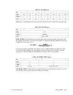
Page 31: ...tor CN18 page 30 LVDS Flat Panel Video Connector CN19 page 31 SATA Disk Chip Socket U6 page 32 Serial Port 1 CN7 and Serial Port 2 CN8 page 33 Advanced Digital I O aDIO Port CN6 page 38 Advanced Analog I O aAIO Port CN10 page 39 USB 2 0 Connector CN17 page 40 Ethernet 10 100 1000Base T and TX Connectors CN20 and CN30 page 41 High Definition Audio CN11 page 42 PCIe 104 Type 2 Bus CN1 Top page 43 PC...

Page 32: ...ngineer Connector Locations Figure 5 shows the connectors and the SATA Disk Chip socket of the CMX32M cpuModule Figure 5 CMX32M Connector Locations Note Pin 1 of each connector is indicated by a white silk screened square on the top side of the board and a square solder pad on the bottom side of the board Pin 1 of the bus connectors match when stacking PC 104 modules SATA Disk Chip U6 HD Audio CN1...

Page 33: ...2x5 0 1 3M 89110 0001 CN6 aDIO 2x8 0 1 3M 89116 0001 CN7 Serial Port 1 COM1 3 2x5 0 1 3M 89110 0001 CN8 Serial Port 2 COM2 4 2x5 0 1 3M 89110 0001 CN10 aAIO Connector 2x5 0 1 3M 89110 0001 CN11 Audio Connector 2x8 0 1 3M 89116 0001 CN13 RTC Battery Input optional 1x2 2mm FCI 69305 002LF CN15 Fan Power switched 1x3 2mm FCI 69305 003LF CN17 USB 2 0 2x5 0 1 3M 89110 0001 CN18 Video SVGA 2x5 2mm 3M 89...

Page 34: ...on must be verified by measuring voltage at the Auxiliary Power Connector and verifying that it does not drop below 4 75 V The voltage at the connector should be checked with an oscilloscope while the system is operational Note Although it is possible to power the cpuModule through the Auxiliary Power connector the preferred method is to power it through the bus connector from a power supply in th...

Page 35: ...is available on pins 1 and 2 of the multi function connector These outputs are controlled by a transistor to supply 0 1 W of power to an external speaker The external speaker should have 8 Ω impedance and be connected between pins 1 and 2 Table 8 Utility Port Connector CN5 Pin Signal Function In Out 1 SPKR Speaker Output open collector out 2 PWR 5 V out 3 RESET Manual Push Button Reset in 4 PWRSW ...

Page 36: ...or System Reset Pin 3 of the multi function connector allows connection of an external push button to manually reset the system The push button should be normally open and connect to ground when pushed The type of reset generated by this button can be set in the BIOS configuration utility Soft Power Button Pin 4 of the multi function connector allows connection of an external push button to send a...

Page 37: ... when system power is removed in order to preserve the date and time in the real time clock Connecting a battery is only requiredtomaintain timewhen power is completely removed from the cpuModule A battery is not required for board operation WARNING The optional RTC battery input connector CN13 should be left unconnected if the multi function connector CN5 has a battery connected to pin 9 ...

Page 38: ...Video Connector CN18 Pin Signal Function In Out 1 VSYNC Vertical Sync out 2 HSYNC Horizontal Sync out 3 DDCSCL Monitor Communications Clock out 4 RED Red Analog Output out 5 DDCSDA Monitor Communications Data bidirectional 6 GREEN Green Analog Output out 7 PWR 5 V out 8 BLUE Blue Analog Output out 9 GND Ground out 10 GND Ground out 9 7 5 3 1 GND PWR DDCSDA DDCSCL VSYNC GND BLUE GREEN RED HSYNC 10 ...

Page 39: ...t 2 Y0M LVDS Data 0 out 3 DDC_CLK1 1 The DDC signals use a 3 3 V signal level and are not 5 V tolerant Panel Detection Clock out 4 GND Ground GND 5 Y1P LVDS Data 1 out 6 Y1M LVDS Data 1 out 7 DDC_DATA1 Panel Detection Data in out 8 GND Ground GND 9 Y2P LVDS Data 2 out 10 Y2M LVDS Data 2 out 11 GND Ground GND 12 GND Ground GND 13 YCP LVDS Clock out 14 YCM LVDS Clock out 15 Y3P LVDS Data 3 out 16 Y3...

Page 40: ...s 1 Always work at an ESD protected workstation and wear a grounded wrist strap 2 Remove power from the system 3 Insert the Disk Chip in the SATA Disk Chip Socket U6 aligning pin 1 with the square solder pad on the board 4 Apply power to the system 5 Re enter the BIOS and set the boot order of the system accordingly Table 14 SATA Disk Chip Socket U6 1 1 TX and RX are the transmit and receive respe...

Page 41: ... 2 kbaud in 16450 and 16550A compatible mode and includes a 16 byte FIFO Refer to any standard PC AT hardware reference for the register map of the UART For more information about programming UARTs refer to Appendix D RS 232 Serial Port Default The default serial port mode is full duplex RS 232 With this mode enabled the serial port connectors must be connected to RS 232 compatible devices Table 1...

Page 42: ...to TXD and connect RXD to TXD When using full duplex typically in RS 422 mode connect the ports as shown in Table 17 When using half duplex in RS 485 mode connect the ports as shown in Table 18 9 7 5 3 1 GND DTR TXD RXD DCD GND RI CTS RTS DSR 10 8 6 4 2 Note The cpuModule has a 120 Ω termination resistor Termination is usually necessary on all RS 422 receivers and at the ends of the RS 485 bus Ter...

Page 43: ... Signal Ground out 5 9 7 5 3 1 GND Rsvd TXD RXD Rsvd GND Rsvd RXD TXD Rsvd 10 8 6 4 2 Note When using the serial port in RS 485 mode the serial transmitters are enabled and disabled under software control The transmitters are enabled by manipulating the Request To Send RTS signal of the serial port controller This signal is controlled by writing bit 1 of the Modem Control Register MCR as follows I...

Page 44: ...ions Connector COM A COM B CN7 COM 1 COM 3 CN8 COM 2 COM 4 Table 21 Dual Serial Port Modes COM A COM B Pinout Reference RS 232 RS 232 Table 22 RS 422 RS 232 Table 23 RS 422 RS 422 Table 24 RS 485 RS 232 Table 23 RS 485 RS 485 Table 24 Table 22 COM A RS 232 and COM B RS 232 Pin Signal Function In Out DB 9 1 DCD1 COM A Data Carrier Detect in 1 2 RXD2 COM B Receive Data in 6 3 RXD1 COM A Receive Data...

Page 45: ...Data out 3 6 RXD1 COM A Receive Data in 8 7 TXD2 COM B Transmit Data out 4 8 RI1 COM A Ring Indicate in 9 9 10 GND Signal Ground 5 Table 24 COM A RS 422 485 and COM B RS 422 485 Pin Signal Function In Out DB 9 1 RXD2 COM B Receive Data in 1 2 RXD2 COM B Receive Data in 6 3 RXD1 COM A Receive Data in 2 4 TXD1 COM A Transmit Data out 7 5 TXD1 COM A Transmit Data out 3 6 RXD1 COM A Receive Data in 8 ...

Page 46: ...ts Interrupts are generated when the 8 bit programmable digital inputs match a pattern or on any value change event Bit masking allows selecting any subgroup of 8 bits The strobe input latches data into the bit programmable port and generates an interrupt Refer to Advanced Digital I O Ports aDIO page 60 for information on programming the aDIO Table 25 aDIO Pinout CN6 Pin Function CN6 Pin Function ...

Page 47: ...en used in conjunction with the aDIO port it allows the cpuModule to be a complete single board data acquisition system For more information on using the aAIO port refer to Advanced Analog I O aAIO page 64 Table 26 aAIO Pinout CN10 Pin Function CN10 Pin Function 1 Channel 1 2 Channel 2 3 Channel 3 4 Channel 4 5 Channel 5 6 Channel 6 7 Channel 7 8 Channel 8 9 GND 10 GND ...

Page 48: ...rated for USB 2 0 such as the cable kit supplied by RTD Table 27 USB Connector CN17 Pin Signal Function In Out 1 VCC1 Supply 5 V to USB1 out 2 VCC2 Supply 5 V to USB2 out 3 DATA1 Bidirectional data line for USB1 in out 4 DATA2 Bidirectional data line for USB2 in out 5 DATA1 Bidirectional data line for USB1 in out 6 DATA2 Bidirectional data line for USB2 in out 7 GND Ground out 8 GND Ground out 9 G...

Page 49: ...nboard 10 100 1000 Ethernet controller Ethernet must be enabled in the BIOS When enabled the multi color LED will blink to indicate an Ethernet connection For more information refer to the Multi Color LED section on page 84 Table 28 Ethernet Connector CN20 RJ 45 Pin 10 Pin DIL Pin Signal Function 3 1 B RX Receive 10 100 6 2 B RX Receive 10 100 4 3 C 5 4 C 1 5 A TX Transmit 10 100 2 6 A TX Transmit...

Page 50: ... 10 Pin DIL Pin Signal Function In Out 1 MIC LIN_L Left Microphone Line Input in 2 MIC LIN_R Right Microphone Line Input in 3 rsvd Reserved 4 GND Signal Ground GND 5 FRONT_L Front Headphone Left Output out 6 FRONT_R Front Headphone Right Output out 7 rsvd Reserved 8 rsvd Reserved 9 REAR_L Rear Left Line Output out 10 REAR_R Rear Right Line Output out 11 CENTER Center Line Output out 12 SUB Sub woo...

Page 51: ...patible before powering the system Table 30 PCIe 104 Type 2 Bus Signal Assignments Top View 1 Pin Signal Signal Pin 1 USB_OC 5 Volts PE_RST 2 3 3 3V 3 3V 4 5 USB_1p USB_0p 6 7 USB_1n USB_0n 8 9 GND GND 10 11 PEx1_1Tp PEx1_0Tp 12 13 PEx1_1Tn PEx1_0Tn 14 15 GND GND 16 17 PEx1_2Tp PEx1_3Tp 18 19 PEx1_2Tn PEx1_3Tn 20 21 GND GND 22 23 PEx1_1Rp PEx1_0Rp 24 25 PEx1_1Rn PEx1_0Rn 26 27 GND GND 28 29 PEx1_2...

Page 52: ... 71 Reserved Reserved 72 73 GND GND 74 75 Reserved Reserved 76 77 Reserved Reserved 78 79 GND GND 80 81 SATA_1Tp SATA_0Tp 82 83 SATA_1Tn SATA_0Tn 84 85 GND GND 86 87 Reserved Reserved 88 89 Reserved Reserved 90 91 GND GND 92 93 Reserved Reserved 94 95 Reserved Reserved 96 97 GND GND 98 99 Reserved Reserved 100 101 Reserved Reserved 102 103 GND GND 104 Table 30 PCIe 104 Type 2 Bus Signal Assignment...

Page 53: ...110 111 Reserved Reserved 112 113 GND GND 114 115 Reserved Reserved 116 117 Reserved Reserved 118 119 GND GND 120 121 Reserved Reserved 122 123 Reserved Reserved 124 125 GND GND 126 127 Reserved Reserved 128 129 Reserved Reserved 130 131 GND GND 132 133 SATA_1Rp SATA_0Rp 134 135 SATA_1Rn SATA_0Rn 136 137 GND GND 138 139 Reserved Reserved 140 141 Reserved Reserved 142 143 GND GND 144 145 Reserved R...

Page 54: ...s on CN1 PCIe Peer To Peer Peer to Peer transactions are transactions directly between two PCIe peripheral cards An example of this is writing data directly from a data acquisition card to a DSP card without first writing to the host CPU s memory The PCIe links that are directly connected to the chipset do not support Peer to Peer transactions The shared PCIe links support peer to peer transaction...

Page 55: ...le before powering the system Table 32 PCIe 104 Type 1 Bus Signal Assignments Top View 1 Pin Signal Signal Pin 1 USB_OC 5 Volts PE_RST 2 3 3 3V 3 3V 4 5 USB_1p USB_0p 6 7 USB_1n USB_0n 8 9 GND GND 10 11 PEx1_1Tp PEx1_0Tp 12 13 PEx1_1Tn PEx1_0Tn 14 15 GND GND 16 17 PEx1_2Tp PEx1_3Tp 18 19 PEx1_2Tn PEx1_3Tn 20 21 GND GND 22 23 PEx1_1Rp PEx1_0Rp 24 25 PEx1_1Rn PEx1_0Rn 26 27 GND GND 28 29 PEx1_2Rp PE...

Page 56: ... 73 GND GND 74 75 PEx16_0T 11 p PEx16_0T 3 p 76 77 PEx16_0T 11 n PEx16_0T 3 n 78 79 GND GND 80 81 PEx16_0T 12 p PEx16_0T 4 p 82 83 PEx16_0T 12 n PEx16_0T 4 n 84 85 GND GND 86 87 PEx16_0T 13 p PEx16_0T 5 p 88 89 PEx16_0T 13 n PEx16_0T 5 n 90 91 GND GND 92 93 PEx16_0T 14 p PEx16_0T 6 p 94 95 PEx16_0T 14 n PEx16_0T 6 n 96 97 GND GND 98 99 PEx16_0T 15 p PEx16_0T 7 p 100 101 PEx16_0T 15 n PEx16_0T 7 n ...

Page 57: ...ilizes the PCIe x16 link is placed directly adjacent to the CPU 105 SDVO_DAT PENA 12 Volts SDVO_CLK 106 107 GND GND 108 109 PEx16_0R 8 p PEx16_0R 0 p 110 111 PEx16_0R 8 n PEx16_0R 0 n 112 113 GND GND 114 115 PEx16_0R 9 p PEx16_0R 1 p 116 117 PEx16_0R 9 n PEx16_0R 1 n 118 119 GND GND 120 121 PEx16_0R 10 p PEx16_0R 2 p 122 123 PEx16_0R 10 n PEx16_0R 2 n 124 125 GND GND 126 127 PEx16_0R 11 p PEx16_0R...

Page 58: ... chipset however only provides five PCIe x1 links Four of the links on CN1 and CN2 are connected directly to the chipset The other four are connected through a PCIe packet switch and share the bandwidth of a single x1 link back to the chipset The links that are connected to the PCIe switchdo not support wake from S3 D3cold Only wakefrom S1 is supported Table 31 below shows the configuration of the...

Page 59: ...quired for board operation Fan Power Switched CN15 The switched fan power connector CN15 is an optional fan connector which allows the system to power the fan when the processor temperature reaches high temperatures To utilize this connector refer to the Thermal Management section on page 81 Table 34 Optional RTC Battery Input CN13 Pin Signal Function 1 BAT RTC Battery Input 2 GND Ground WARNING T...

Page 60: ...52 CMX32M cpuModule BDM 610000075 Rev B ...
Page 61: ...e following topics The RTD Enhanced AMI BIOS page 54 Memory Map page 56 I O Address Map page 57 Hardware Interrupts page 58 Advanced Digital I O Ports aDIO page 60 Advanced Analog I O aAIO page 64 Real Time Clock Control page 78 Watchdog Timer Control page 80 Thermal Management page 81 Power Management page 82 Multi Color LED page 84 Reset Status Register page 85 Features and Settings That Can Aff...

Page 62: ...hardware and the OS which is in control It is active from the time the OS boots until the cpuModule is turned off The CORE BIOS provides the system with a series of software interrupts to control various hardware devices Configuring the RTD Enhanced AMI BIOS The cpuModule Setup program allows you to customize the cpuModule s configuration Selections made in Setup are stored on the board and are re...

Page 63: ...nd PCI options and control system resources Boot Press Enter to select Set the system boot sequence Security Press Enter to select Setup the supervisor and user access passwords or enable boot sector virus protection Power Press Enter to select Control power management settings including power supply type and system wake functions Thermal Press Enter to select Monitor the cpuModule temperature or ...

Page 64: ...mory managers Table 38 First Megabyte Memory Map Address hex Description C0000 FFFFFh ROM 256 KB BIOS in Flash EPROM shadowed into DRAM during runtime C0000 EFFFFh Run time user memory space Usually memory between C0000h and CFFFFh is used for the BIOS of add on VGA video cards A0000 BFFFFh Normally used for video RAM as follows EGA VGA Monochrome CGA 0A0000 0AFFFFh 0B0000 0B7FFFh 0B8000 0BFFFFh 0...

Page 65: ... Addresses Reserved for the CMX32M cpuModule Address Range hex Bytes Device 000 00Fh 16 DMA Controller 010 01Fh 16 Reserved for CPU 020 021h 2 Interrupt Controller 1 022 02Fh 13 Reserved 040 043h 4 Timer 060 064h 5 Keyboard Interface 070 071h 2 Real Time Clock Port 080 08Fh 16 DMA Page Register 0A0 0A1h 2 Interrupt Controller 2 0C0 0DFh 32 DMA Controller 2 0F0 0FFh 16 Math Coprocessor 100 101h 2 V...

Page 66: ...t Normal Use 0 Timer 0 1 Keyboard 2 Cascade of IRQ 8 15 3 COM2 4 COM1 5 Available 6 Available 7 Available 8 Real Time Clock 9 Available routed to IRQ 2 10 Available 11 Available 12 Mouse 141 1 IRQs 14 and 15 may be available if the SATA controller is not configured in Compatability Mode SATA hard disk 151 SATA Disk Chip socket Note The cpuModule has onboard PCI devices that will claim IRQ lines In...

Page 67: ...f the non standard divisors 460 800 921 600 and 1 500 000 If the result is a whole number substitute that value for the Divisor Latch Low Byte For example to achieve a baud rate of 750 000 select the Divisor Latch High Byte for 1 500 000 and set the Divisor Latch Low Byte to 2 Table 41 Divisor Latch High and Low Bytes Divisor Latch High Byte Divisor Latch Low Byte Baud Rate Error Bit 7 Bit 6 Bit 5...

Page 68: ...ata Port 1 data Multi Function DIO Control and Wake Control register Digital I O Register Set Port 0 Data register is a read write bit direction programmable register A particular bit can be set to input or output A read of an input bit returns the value of port 0 A read of an output bit returns the last value written to Port 0 A write to an output bit sends that value to port 0 Port 1 Data regist...

Page 69: ...masked off are compared against the value on Port 0 A Match or Event causes bit 6 of DIO Control to be set and if the aDIO is in Advanced interrupt mode the Match or Event causes an interrupt Table 45 DIO Control I O Address 9C3h Read Access D7 D6 D5 D4 D3 D2 D1 D0 Table 46 DIO Control I O Address 9C3h Write Access D7 D6 D5 D4 D3 D2 D1 D0 Table 47 Multi Function at Address 9C2h1 1 Contents based o...

Page 70: ...logic The deglitching requires pulses on Port 0 to be at least 120 ns in width As long as changes are present longer than that the event is guaranteed to register Pulses as small as 60 ns can register as an event but they must occur between the rising and falling edge of the 8 33 MHz clock To enter Event mode set bits 4 3 of the DIO Control register to 10 Match Mode When this mode is enabled Port ...

Page 71: ...PU from any power down mode including Soft Off S5 Wake from aDIO will work as long at 5V Standby power is applied to the board To use the aDIO to wake the system Wake from aDIO must first be enabled in the BIOS setup utility Then the aDIO is configured in the appropriate interrupt mode The Wake Enable bit is then set in the Wake Control Register at 0x9C4 The CPU can then be placed in a standby mod...

Page 72: ...ction generates an interrupt when signal crosses high or low threshold Advanced DMA Each channel has it s own DMA buffer Buffer chaining prevents interrupt latency problems DMA to anywhere in 4GB address space Block Diagram The Figure below shows the functional block diagram of aAIO The various parts of the block diagram are discussed in the following sections Figure 7 aAIO Block Diagram Range Gai...

Page 73: ...a NEXT_CHANNEL of 0 Otherwise the channels will continue to scan without waiting for the pacer clock The Channel Gain Table contains all of the channel specific settings and status This includes the mode single ended or differential and range It also contains the filter and threshold setting as well as the interrupt status and enable bits The A D Result register which returns the last conversion f...

Page 74: ...terrupt when a channel crosses a high or low threshold The thresholds can be individually set and monitored for each channel Threshold crossings are only detected for a channel when that channel is sampled Table 50 Filter Cutoff Frequency ORDER 3 dB Cutoff 0 n a 1 0 114791 fs 2 0 045995 fs 3 0 021236 fs 4 0 010255 fs 5 0 005042 fs 6 0 002501 fs 7 0 001246 fs ...

Page 75: ...of the SGT and the same offset for all channels This guarantees that the captured data is synchronized The DMA engine will always iterate through the SGT even if DMA is not enabled for any channels The Scatter Gather Table is not cleared at power up or during reset Therefore software must assume that it contains random invalid data Operating Modes Simple Operation The simplest operating mode is us...

Page 76: ...tter Gather table 4 Write channel and input configuration in CGT Register if needed default is 10V single ended 5 Start conversion 6 Wait for DMA interrupt 7 Update Scatter Gather table if needed 8 Process or move data if needed 9 Repeat to Step 6 Registers Register Map Table 51 aAIO Register Map Name I O Port 31 24 23 16 15 8 7 0 Control 0x09E0 CH_IRQ_ENA CH_IRQ_STAT MODE_RESET SELECT 3 0 Pacer C...

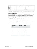
Page 77: ... sampling clear the Filters and reset the Scatter Gather and DMA Offset counters Always reads 0 Chx A 1 indicates that an interrupt is pending from channel x of the Channel Gain Table This bit is set regardless ofCH_IRQ_ENA This is a non stick register andwill becleared whenthe interruptconditionis cleared in the Channel Gain Table 0x9E0 SELECT Register Bit 7 6 5 4 3 2 1 0 Mode R R R R R R W R W R...

Page 78: ...CER_DIVIDER value that would yield a sample rate of greater than 100kHz has undefined results except a PACER_DIVIDER value of 0x00000000 will sample at the fastest rate possible CUR_BUFFER_OFFSET The offset into the current 4kB DMA buffer where data will be written next This is the same value for every channel i e the channels are always synchronized 0x9E3 CH_IRQ_ENA Register Bit 7 6 5 4 3 2 1 0 M...

Page 79: ...an The NEXT_CHANNEL pointer is followed until it is a value of 0 which ends the scan There are a few implications 1 The first channel to be scanned must always be Channel 1 2 Each channel may only be sampled once per scan 3 The scan list must end with a NEXT_CHANNEL of 0 Otherwise the channels will continue to scan without waiting for the pacer clock The channel associations for CGT_CHANNEL and NE...

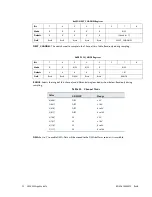
Page 80: ...moved to the DMA buffer as soon as it is available 0x9EC NEXT_CHANNEL Register Bit 7 6 5 4 3 2 1 0 Mode R R R R R R W Default 0 0 0 0 0 Channel 1 Field Rsvd Rsvd Rsvd Rsvd Rsvd NEXT_CHANNEL 0x9ED CH_MODE Register Bit 7 6 5 4 3 2 1 0 Mode R R R W R W R R W Default 0 0 0 0 0 101 Field Rsvd Rsvd DMA Rsvd Rsvd RANGE Table 53 Channel Mode Value SE DIFF Range 0 000 DIFF 5V 1 001 DIFF 10V 2 010 DIFF 0 to...

Page 81: ...filtering This is a 32 bit 2 s complement value with same 76 294 microvolt resolution for all ranges 0x9EE SGT_ROW Register Bit 7 6 5 4 3 2 1 0 Mode R R W Default 0 0 Field Reserved SGT_ROW 0x9EF FILTER_CON Register Bit 7 6 5 4 3 2 1 0 Mode R R R R R R W Default 0 0 0 0 0 0 Field Rsvd Rsvd Rsvd Rsvd Rsvd ORDER 0x9F0 AD_RESULT Register Bit 31 0 Mode R Default 0x00000000 Field AD_RESULT Range Bits 3...

Page 82: ... corresponding bit in IRQ_STAT is set Sample A sample has been converted DMA An SGT row with the IRQ bit set has been filled DMA Error DMA for this channel didn t get serviced in time gap in data Thresh Low Channel is below the low threshold Thresh High Channel is above the high threshold 0x9F4 IRQ_STAT Register Bit 7 6 5 4 3 2 1 0 Mode R R R C R C R C R C R R C Default 0 0 0 0 0 0 0 0 Field Rsvd ...

Page 83: ...threshold the IRQ_STAT Thresh Low bit is set THRESH_HIGH This register sets the high threshold for this channel It contains a 16 bit 2 s complement value with the same 305 175 microvolt resolution 20V 65536 for all ranges The high threshold must be greater than low threshold The default for the high threshold is the maximum positive value If the A D reading for this channel is greater than the hig...

Page 84: ...ble is not cleared at power up or during reset Therefore software must assume that it contains random invalid data ADDRESS The upper 20 bits of a DMA buffer 4k in size and 4k aligned The DMA data will start at an offset of 0 into the buffer After it is full the DMA engine will advance to the next row in the table based on the flags IRQ Flag to generate and interrupt after this buffer is full The i...

Page 85: ...a will be available for the first sample 1 Perform a Board Reset to make sure all the registers are default 2 Do a software triggered sample 3 Wait for it to be done 4 Perform a Board Reset to reset the sample counter Changing Ranges The channel ranges are only actually updated during sampling If for example you are sampling a 3V signal in the 0 5V range then stop sampling connect a 9V signal and ...

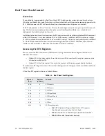
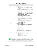
Page 86: ...hanced BIOS also mirrors the user settings from flash in CMOS Therefore the contents of CMOS may be overwritten at boot time and should be treated as read only Accessing the RTC Registers You may access the RTC date time and CMOS memory using the Index and Data Registers located at I O addresses 70h and 71h Address 70h is the Index register It must be written with the number of the register to rea...

Page 87: ...is bit low and let the operating system manage time zones and DST 0Ch 12 RTC Status Register C Read Only Bit 7 IRQ Flag Indicates that the Real Time Clock IRQ is asserted Goes high whenever one of the enabled interrupt conditions in Register B occurs Bit 6 Periodic Flag Bit 5 Alarm Flag Bit 4 Update Ended Flag Bit 3 0 Reserved Reading this register will also clear any of set flag IRQ Periodic Alar...

Page 88: ...of the reset time out period or half of the interrupt time out period whichever is applicable Register Description The Advanced Watchdog Timer has a Setup Register and a Runtime Register The Setup Register is set by the BIOS and can be adjusted by entering the BIOS Setup Utility and going to Advanced Miscellaneous RTD Features The Setup Register may also be read by the driver to determine if the W...

Page 89: ...he CPU s power consumption is reduced and the life of the fan is increased Always On When in this mode the fan is always powered by the CPU On At 70C This mode allows the system to keep the fan turned off until the CPU reaches 70C In this mode the fan will slowly transition between on and off to prevent oscillations This is the best mode for applications that will spend most of the time below 0C V...

Page 90: ...n this mode the CPU stops executing instructions but power to the CPU and RAM is maintained S3 Suspend to RAM Everything in the system is powered off except for the system memory When the system wakes from this mode operating systems allow applications to resume where they left off as the state of the application is preserved in memory S4 Hibernate When the system enters this state the operating s...

Page 91: ...ed off i e during Suspend to RAM S3 Hibernate S4 or Soft Off S5 power modes The PSON signal is an active low open drain output that signals the power supply to turn on Use of these signals allows the power consumption to drop to below 1W during standby modes and still enable any of the wake events Reducing Power Consumption In addition to the CPU s low power modes power consumption can further be ...

Page 92: ...odule is in reset1 1 If power is applied to the cpuModule while jumper JP5 is installed the LED will be red This does not indicate that the board is in reset Yellow Red Green cpuModule is in Standby White R G B cpuModule is approaching thermal limit2 2 The LED will remain White until the system is shut down Table 58 Multi Color LED I O Address 984h D7 D6 D5 D4 D3 D2 D1 D0 Reserved Reserved Reserve...

Page 93: ...t can be cleared by writing a 1 to the selected bit of I O port 0x987 Utility Reset 1 reset asserted 0 no reset System Power Good 1 reset asserted 0 no reset Main 5V Input 1 reset asserted 0 no reset Memory Power 1 reset asserted 0 no reset CPU Core Power 1 reset asserted 0 no reset SIO Power Good 1 reset asserted 0 no reset Management Power 1 reset asserted 0 no reset Standby Power 1 reset assert...

Page 94: ...et2 2 The BIOS allows the user to change the function of the utility connector s push button reset Even if the push button is not configured as a reset this bit will always read a 1 asserted when the reset button has been pushed D6 CPU Core Power 5 CPU core powers supply D5 System Power 4 Power supplies that are not for standby power D4 SIO Power 3 Power monitored by the Super I O D3 Main Power 5V...

Page 95: ...ke some time to initialize the VGA BIOS Exactly how long will depend on the particular VGA controller and BIOS version Hard Drive Type During Hard Drive initialization each device must be probed Some devices take longer to probe 2 5 inch hard drives tend to take longer than 3 5 inch ones because they spin at a lower RPM Monitor Type Some monitors take a while to power on Desktop flat panels are es...

Page 96: ... BIOS Serial Power On Self Test POST Code Output The POST Codes represents a series of events that take place in a system during the Power On Self Test If the POST fails the system will not boot as expected Knowing which POST code the failure occurred may help system debug This recovery mode configures serial port connector CN3 as dual RS 232 and sends the POST codes on the second port i e pin 7 i...

Page 97: ...ndix A Hardware Reference 89 Appendix A Hardware Reference This appendix provides information on CMX32M cpuModule hardware including Jumper Settings and Locations page 90 Onboard PCI Devices page 92 Physical Dimensions page 93 ...

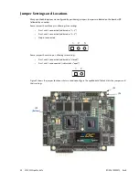
Page 98: ...e pins allowing three settings Pins 1 and 2 connected indicated as 1 2 Pins 2 and 3 connected indicated as 2 3 No pins connected Some jumpers have two pins allowing two settings Pins 1 and 2 connected indicated as closed Pins 1 and 2 unconnected indicated as open Figure 9 shows the jumper locations that are used to configure the cpuModule Table 64 lists the jumpers and their settings 1 2 3 1 2 JP9...

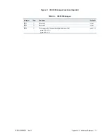
Page 99: ... Reference 91 Figure 9 CMX32M Jumper Locations top side Table 64 CMX32M Jumpers Jumper Pins Function Default JP5 2 Reserved open JP6 2 Reserved open JP9 3 Select power for flat panel backlight bottom side pins 1 2 12 V pins 2 3 5 V pins 2 3 ...

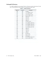
Page 100: ...ay Controller 10F5 8086 Ethernet Controller CN20 2937 8086 USB UHCI 4 2938 8086 USB UHCI 5 2939 8086 USB UHCI 6 293C 8086 USB EHCI 2 293E 8086 HD Audio Controller 2940 8086 PCI to PCI Bridge PCIe 104 x1 1 2942 8086 PCI to PCI Bridge PCIe 104 x1 2 2944 8086 PCI to PCI Bridge PCIe 104 x1 3 2946 8086 PCI to PCI Bridge PCIe 104 x1 4 2948 8086 PCI to PCI Bridge to Shared Links 2934 8086 USB UHCI 1 2935...

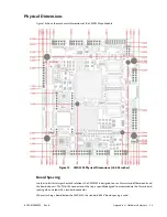
Page 101: ...ions 0 005 inches Board Spacing In order to facilitate larger heatsink solutions the CMX32M is designed to use a 22mm standoff between it and the board above it The PCIe 104 connector on the top is specially designed to accommodate the 22mm board spacing when mated with a standard connector When attaching a board below the CMX32M the standard 0 600 board spacing is used ...

Page 102: ...94 CMX32M cpuModule BDM 610000075 Rev B ...
Page 103: ...you may encounter with operation of your CMX32M cpuModule are due to common errors This appendix includes the following sections to help you get your system operating properly Common Problems and Solutions page 96 Troubleshooting a PC 104 System page 97 How to Obtain Technical Support page 98 ...

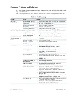
Page 104: ...h power not connected to boot drive connect power cable to floppy or hard drive erratic operation excessive bus loading reduce number of modules in stack remove termination components from bus signals remove any power supply bus terminations power supply noise examine power supply output with oscilloscope glitches below 4 75 VDC will trigger a reset add bypass caps power supply limiting examine po...

Page 105: ...on consult drive documentation floppy does not work data error due to drive upside down orient drive properly upright or on side will not boot when video card is removed illegal calls to video controller look for software trying to access nonexistent video controller for video sound or beep commands abnormal video flat panel is enabled disable the flat panel in the BIOS can only use 640 x 480 reso...

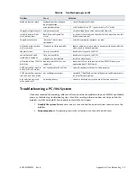
Page 106: ... gather the following information cpuModule model BIOS version and serial number List of all boards in system List of settings from cpuModule Setup program Printout of autoexec bat and config sys files if applicable Description of problem Circumstances under which problem occurs Then contact RTD Technical Support Phone 814 234 8087 Fax 814 234 5218 E mail techsupport rtd com ...

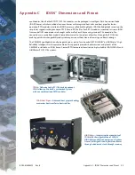
Page 107: ...other than through the PC 104 bus enabling quick interchangeability and system expansion without hours of rewiring and board redesign The CMX32M cpuModule can also be purchased as part of a custom built RTD HiDAN or HiDANplus High Reliability Intelligent Data Acquisition Node This appendix provides the dimensions and pinouts of the CMX32M installed in an IDAN frame Contact RTD for more information...

Page 108: ...g P N Adam Tech DE09SD 15 pin D female module P N Adam Tech DB15SD mating P N Adam Tech DB15PD 6 pin mini DIN female module P N Adam Tech MDE006W mating P N Adam Tech MDP006 REAR 15 pin high density D female module P N Adam Tech HDT15SD mating P N Adam Tech HDT15PD 20 pin mini D female module P N 3M 10220 6212VC mating P N 3M 10120 3000VE 9 pin D male module P N Adam Tech DE09PD mating P N Adam Te...

Page 109: ...e 6 Pin mini DIN Connector female IDAN Pin Signal Function 1 MDAT Mouse Data 2 Reserved 3 GND Ground 4 5 V 5 Volts 5 MCLK Mouse Clock 6 Reserved Table 68 Keyboard 6 Pin mini DIN Connector female IDAN Pin Signal Function 1 KDAT Keyboard Data 2 Reserved 3 GND Ground 4 5 V 5 V 5 KCLK Keyboard Clock 6 Reserved ...

Page 110: ...put 4 DTR Data Terminal Ready Output 5 GND Ground 6 DSR Data Set Ready Input 7 RTS Request To Send Output 8 CTS Clear To Send Input 9 RI Ring Indicator Input Table 70 COM1 COM2 RS 422 485 9 Pin D Connector male IDAN Pin Signal Function Mode 1 Reserved 2 RXD Receive Data Input 3 TXD Transmit Data Output 4 Reserved 5 GND Ground 6 Reserved 7 TXD Transmit Data Output 8 RXD Receive Data Input 9 Reserve...

Page 111: ...or female IDAN Pin aDIO Port CPU Pin 1 P0 0 1 2 P0 1 2 3 P0 2 3 4 P0 3 4 5 P0 4 5 6 P0 5 6 7 P0 6 7 8 P0 7 8 9 Strobe 0 9 10 Strobe 1 10 11 P1 0 11 12 P1 1 12 13 P1 2 13 14 P1 3 14 15 GND 15 16 5V 16 17 reserved 18 reserved 19 GND 20 GND 21 GND 22 GND 23 GND 24 reserved 25 reserved 26 reserved ...

Page 112: ...nnel 4 4 8 Channel 6 6 9 Channel 8 8 Table 73 Panel 20 Pin mini D Connector female IDAN Pin Signal Name CPU Pin 1 LVDS_YAP0 1 2 LVDS_DDCPCLK 3 3 LVDS_YAP1 5 4 LVDS_DDCPDATA 7 5 LVDS_YAP2 9 6 GND 11 7 LVDS_CLKAP 13 8 LVDS_YAP3 15 9 GND 17 10 FP_BKLT 19 11 LVDS_YAM0 2 12 GND 4 13 LVDS_YAM1 6 14 GND 8 15 LVDS_YAM2 10 16 GND 12 17 LVDS_CLKAM 14 18 LVDS_YAM3 16 19 FP_VCC 18 20 LVDS_BKLTCTL 20 ...

Page 113: ...tion CPU Pin 1 Red Red Analog Output 4 2 Green Green Analog Output 6 3 Blue Blue Analog Output 8 4 Reserved Reserved 5 GND Ground 9 6 GND Ground 9 7 GND Ground 9 8 GND Ground 10 9 5 V 5 Volts 7 10 GND Ground 10 11 Reserved Reserved 12 DDC Data Monitor data 5 13 HSYNC Horizontal Sync 2 14 VSYNC Vertical Sync 1 15 DDC CLK Monitor Clock 3 ...

Page 114: ...Data input output 3 Data USB1 USB1 Data input output 4 GND Ground 5 GND Ground 6 VCC2 5 V to USB2 output 7 Data USB2 USB2 Data input output 8 Data USB2 USB2 Data input output 9 GND Ground Table 76 Ethernet 9 Pin D Connector female IDAN Pin RJ 45 Pin Signal CPU Pin 1 3 B RX 1 2 4 C 3 3 1 A TX 5 4 7 D 7 5 Ground 9 6 6 B RX 2 7 5 C 4 8 2 A TX 6 9 8 D 8 ...

Page 115: ...Reserved 3 4 GND Signal Ground GND 4 5 FRONT_L Front Headphone Left Output out 5 6 FRONT_R Front Headphone Right Output out 6 7 rsvd Reserved 7 8 rsvd Reserved 8 9 REAR_L Rear Left Line Output out 9 10 REAR_R Rear Right Line Output out 10 11 CENTER Center Line Output out 11 12 SUB Sub woofer Output out 12 13 SP_OUT S PDIF Digital output out 13 14 GND Signal Ground GND 14 15 rsvd Reserved 15 16 GND...

Page 116: ...108 CMX32M cpuModule BDM 610000075 Rev B ...
Page 117: ...ms for this cpuModule refer to the RTD website Interrupt Programming For more information about interrupts and writing interrupt service routines refer to the following book Interrupt Driven PC System Design by Joseph McGivern ISBN 0929392507 Serial Port Programming For more information about programming serial port UARTs consult the following book Serial Communications Developer s Guide by Mark N...

Page 118: ...110 CMX32M cpuModule BDM 610000075 Rev B ...
Page 119: ...Technologies or as a result of service or modification by anyone other than RTD Embedded Technologies Except as expressly set forth above no other warranties are expressed or implied including but not limited to any implied warranties of merchantability and fitness for a particular purpose and RTD Embedded Technologies expressly disclaims all warranties not stated herein All implied warranties inc...

Page 120: ...112 CMX32M cpuModule BDM 610000075 Rev B ...
Reviews: