
RTD Embedded Technologies, Inc.
| www.rtd.com
27
DM35418HR/DM35218HR
User’s Manual
BDM-610010041 Rev F
5
Functional Description
5.1
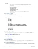
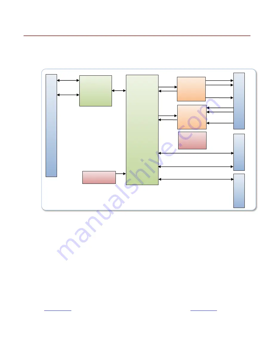
Block Diagram
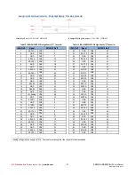
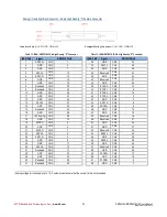
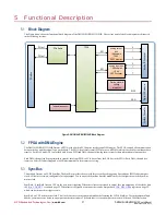
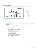
The Figure below shows the functional block diagram of the DM35418HR/DM35218HR. The various parts of the block diagram are discussed
in the following sections.
Figure 8: DM35418HR/DM35218HR Block Diagram
5.2
FPGA with DMA Engine
The DM35418HR/DM35218HR features a FPGA with a built in PCI Express interface and DMA engine. The FPGA controls all communication
between the bus and the control logic on the board. The FPGA also features small FIFOs for use with DMA, which is needed for continuous data
transfer. Each DAC and ADC is provided with its own FIFO and DMA channel, allowing them to transfer data independent of one another.
Each DMA channel can be programmed to transfer data from FPGA to PCIe bus or from the PCIe bus to the FPGA. Each DMA channel also
features a 64-bit PCI addressing and a 16MB maximum buffer for memory accessing.
5.3
SyncBus
This module features an LVDS SyncBus. The SyncBus provides the user with three event based triggering lines and one 10MHz based master
clock. All four are software configurable for input/output. To use any of the SyncBus lines the module must be configured to use the SyncBus
master clock.
SyncBus0 – SyncBus2 lines on CN5 are the user event triggering. When these lines are assigned as output, they can output any of the clocks find
in
section on page 52. When lines are assigned as an input, they can be assigned as a
register on page 52,
which can be then used to trigger events.
SyncBus3 on CN5 is the master clock. This clock is used to synchronize multiple boards featuring the LVDS SyncBus. To synchronize multiple
boards, you must set one board as an output and the rest as inputs. The board that is set as an output, the master will drive a 10MHz clock on
FPGA
Analog input with
1.5 Msample/s
18 bit
ADC Converter
0
…
7
Analog output
with
1Msample/s
16bit
DAC Converter
SPI
….
0
7
PC
Ie
B
us
Temperature sensor
An
alo
g
I/O
C
on
ne
ct
or
1
1
Precise onboard
voltage
references
DIO 0
DIO 31
…
D
ig
ita
l I
/O
C
on
ne
ct
or
PCIe x1
PCIe Switch
SPI
Sy
nc
Bu
s
C
on
ne
ct
or
PCIe x1


