background image


RTD Embedded Technologies, Inc. 

www.rtd.com 


31


DM35418HR/DM35218HR

 User’s Manual 


BDM-610010041 Rev F


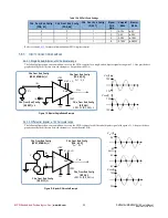
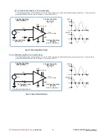
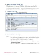
5.4.3.3. Single Ended, Unipolar, 0-10V Full-scale range 

The following figure shows an example how to set up the FPGA registers for a single-ended, unipolar signal with a gain of 1. Also provided are 
graphs showing the difference between the input vs. output from the PGA. 


Figure 12: Unipolar Single Ended Example 


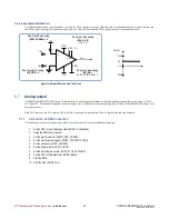
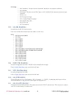
5.4.3.4. Differential, Unipolar, 0-10V Full-scale range 

The following figure shows an example how to set up the FPGA registers for a differential, unipolar signal with a gain of 1. Also provided are 
graphs showing the difference between the input vs. output from the PGA. 


Figure 13: Unipolar Differential Example 


VREF 

CHn_Front_End_Config 

[PGA_A[1:0]] 

G=1

 :

 0, 0 


+15V 

-15V 

IN+ 


IN- 


A1 A0 -> G 

Gain 


CHn_Front_End_Config 

[BIP_UNI] 

VREF: -5V: [BIP_UNI] = 1 


CHn_Front_End_Config 

[VREF_NORMAL] = 1 

CHn_Front_End_Config 

[SE_DIFF] = 0 

V

in


V

PGA


10V 

V

in

(t) 

V

PGA

(t) 

5V 

-5V 

5V 
 

VREF 

CHn_Front_End_Config 

[PGA_A[1:0]] 

G=1

 :

 0, 0 


+15V 

-15V 

IN+ 


IN- 


A1 A0 -> G 

Gain 


CHn_Front_End_Config 

[BIP_UNI] 

VREF: -5V: [BIP_UNI] = 1 


CHn_Front_End_Config 

[VREF_NORMAL] = 1 

CHn_Front_End_Config 

[SE_DIFF] = 1 

V

in


V

PGA


External Ground Reference Resistor 

10V 

V

in

(t) 

V

PGA

(t) 

5V 

-5V 

5V 
Summary of Contents for DM35218HR

Page 1: ...RTD Embedded Technologies Inc AS9100 and ISO 9001 Certified DM35418HR DM35218HR PCI Express Data Acquisition Board User s Manual BDM 610010041 Rev F...

Page 2: ...rtd com ii DM35418HR DM35218HR User s Manual BDM 610010041 Rev F RTD Embedded Technologies Inc 103 Innovation Boulevard State College PA 16803 USA Telephone 814 234 8087 Fax 814 234 5218 www rtd com...

Page 3: ...ty of their respective owners Failure to follow the instructions found in this manual may result in damage to the product described in this manual or other components of the system The procedure set f...

Page 4: ...16 Other Connectors 16 3 3 3 Jumpers 16 3 3 4 LEDs 17 LED 0 Clock Reset 17 LED 1 Clock Status 17 LED 2 SYNCBUS Lock 17 LED 3 Clock Select 17 3 4 Steps for Installing 18 4 IDAN Connections 19 4 1 Modul...

Page 5: ...Only 35 6 1 6 GBC_SYS_CLK_FREQ Read Only 35 6 1 7 GBC_USER_ID Read Only 36 6 1 8 GBC_IRQ_STATUS Read Clear 36 6 1 9 GBC_DIRQ_STATUS Read Clear 36 6 1 10 GBC_EOI Read Clear 36 6 1 11 FBn_ID Read Only 3...

Page 6: ...ad Write 46 6 5 6 CLK_DIV Read Write 46 6 5 7 CLK_DIV_CNTR Read Only 46 6 5 8 POST_STOP_CONVERSIONS Read Write 47 6 5 9 CONVERSION_CNT Read Only 47 6 5 10 INT_ENA Maskable Read Write 47 6 5 11 INT_STA...

Page 7: ...4 Functional Characteristics 11 Table 5 CN3 Single Ended Mode Pin out 15 Table 6 CN4 Differential Mode Pin out 16 Table 7 CN4 Single Ended Mode Pin out 16 Table 8 CN5 Pin out 16 Table 9 IDAN DM35418...

Page 8: ...and messages o Message Signaled Interrupt MSI support Analog inputs o 4 8 channels high speed inputs with independent sampling or simultaneous sampling o 1 538 MSPS maximum input sampling rate o 18 bi...

Page 9: ...a custom built RTD HiDAN or HiDANplus High Reliability Intelligent Data Acquisition Node Contact RTD sales for more information on our high reliability systems 1 4 Contact Information 1 4 1 SALES SUPP...

Page 10: ...77 A DM35218HR Active 1 18 A PCIe 104 Bus Differential Output Voltage 0 8 1 2 V DC Differential TX Impedance 80 120 Differential Input Voltage 0 175 1 2 V DC Differential RX Impedance 80 120 Electric...

Page 11: ...12mA 0 0 4 V VOH Output High Voltage IO 12mA 2 4 3 3 V 3 3V Output CN3 100 mA SyncBus LVDS Differential Input Voltage 2 4 V Input Voltage Threshold 0 05 0 05 V Differential Output Voltage IO 4 A 0 48...

Page 12: ...ated using a Blackman Hanning three term window Figure 1 Channel FFT 2 1 2 ANALOG INPUT HISTOGRAMS In Figure 2 you can see a histogram of samples from sampling a grounded input in 10 V differential in...

Page 13: ...our system When removing it from the bag hold the board at the edges and do not touch the components or connectors Handle the board in an antistatic environment and use a grounded workbench for testin...

Page 14: ...ctor The PCIe connector is the connection to the system CPU The position and pin assignments are compliant with the PCI 104 Express Specification See PC 104 Specifications on page 54 The DM35418HR DM3...

Page 15: ...able 5 CN3 Single Ended Mode Pin out DIO0 1 2 1 DIO0 0 DIO0 3 4 3 DIO0 2 DIO0 5 6 5 DIO0 4 DIO0 7 8 7 DIO0 6 DIO0 9 10 9 DIO0 8 DIO0 11 12 11 DIO0 10 DIO0 13 14 13 DIO0 12 DIO0 15 16 15 DIO0 14 GND 18...

Page 16: ...d Mode Pin out No Connect 2 1 ADC0 0 GND 4 3 GND No Connect 6 5 ADC1 0 GND 8 7 GND No Connect 10 9 ADC2 0 GND 12 11 GND No Connect 14 13 ADC3 0 GND 16 15 GND Reserved 18 17 Reserved GND 20 19 GND Rese...

Page 17: ...t When on the system clock is no longer in reset LED 1 Clock Status This LED blinks when the systems clock is running LED 2 SYNCBUS Lock This LED is on when using the SYNCBUS and the clock is locked L...

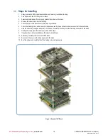
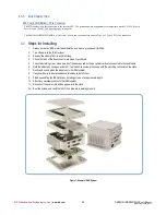
Page 18: ...nnector are properly positioned 6 Check the stacking order make sure all of the busses used by the peripheral cards are connected to the cpuModule 7 Hold the module by its edges and orient it so the b...

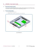
Page 19: ...you are ready to install it into your system When removing it from the bag hold the module by the aluminum enclosure and do not touch the components or connectors Handle the module in an antistatic en...

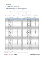
Page 20: ...4 21 22 ADC5 0 CN4 22 23 GND CN4 23 24 GND CN4 24 25 ADC6 0 CN4 25 26 ADC6 0 CN4 26 27 GND CN4 27 28 GND CN4 28 29 ADC7 0 CN4 29 30 ADC7 0 CN4 30 31 GND CN4 31 32 GND CN4 32 33 DAC0 0 CN4 33 34 GND CN...

Page 21: ...SYNC0 CN5 1 22 ADC0 0 CN4 2 23 ADC1 0 CN4 5 24 GND CN4 8 25 GND CN4 11 26 ADC3 0 CN4 14 27 ADC4 0 CN4 17 28 GND CN4 20 29 GND CN4 23 30 ADC6 0 CN4 26 31 ADC7 0 CN4 29 Table 10 IDAN DM35418 62 Pin Hig...

Page 22: ...CN4 7 5 DIO0 8 CN4 9 6 DIO0 10 CN4 11 7 DIO0 12 CN4 13 8 DIO0 14 CN4 15 9 GND CN4 17 10 DIO0 16 CN4 19 11 DIO0 18 CN4 21 12 DIO0 20 CN4 23 13 DIO0 22 CN4 25 14 DIO0 24 CN4 27 15 DIO0 26 CN4 29 16 DIO0...

Page 23: ...ed CN4 22 23 GND CN4 23 24 GND CN4 24 25 Reserved CN4 25 26 Reserved CN4 26 27 GND CN4 27 28 GND CN4 28 29 Reserved CN4 29 30 Reserved CN4 30 31 GND CN4 31 32 GND CN4 32 33 DAC0 0 CN4 33 34 GND CN4 34...

Page 24: ...CN5 1 22 ADC0 0 CN4 2 23 ADC1 0 CN4 5 24 GND CN4 8 25 GND CN4 11 26 ADC3 0 CN4 14 27 Reserved CN4 17 28 GND CN4 20 29 GND CN4 23 30 Reserved CN4 26 31 Reserved CN4 29 Table 13 IDAN DM35218 62 Pin Hig...

Page 25: ...CN4 7 5 DIO0 8 CN4 9 6 DIO0 10 CN4 11 7 DIO0 12 CN4 13 8 DIO0 14 CN4 15 9 GND CN4 17 10 DIO0 16 CN4 19 11 DIO0 18 CN4 21 12 DIO0 20 CN4 23 13 DIO0 22 CN4 25 14 DIO0 24 CN4 27 15 DIO0 26 CN4 29 16 DIO0...

Page 26: ...DAN system 3 Remove the module from its anti static bag 4 Check that pins of the bus connector are properly positioned 5 Check the stacking order make sure all of the busses used by the peripheral car...

Page 27: ...3 SyncBus This module features an LVDS SyncBus The SyncBus provides the user with three event based triggering lines and one 10MHz based master clock All four are software configurable for input outpu...

Page 28: ...module also provides 28V overvoltage input protection to the analog connector CN4 The DM35418HR DM35218HR has a programmable input This provides the user the ability to select single ended differenti...

Page 29: ...MA 10 Start the ADC MODE Go 5 6 2 SIMPLIFIED BLOCK DIAGRAM OF ANALOG INPUT The following figure shows the front end circuit for the DM35418HR DM35218HR It also shows the names of the FPGA registers in...

Page 30: ...erence between the input vs output from the PGA 5 4 3 2 Differential Bipolar 10V Full scale range The following figure shows an example how to set up the FPGA registers for a differential bipolar sign...

Page 31: ...ow to set up the FPGA registers for a differential unipolar signal with a gain of 1 Also provided are graphs showing the difference between the input vs output from the PGA Figure 13 Unipolar Differen...

Page 32: ...AC converter has a 511 sample FIFO for DMA Each sample is packed into 32 bits right justified and sign extended 5 7 1 INITIALIZING THE DAC CONVERTER The following is a list of the typical steps needed...

Page 33: ...1 1 8 n a Table 17 Key DAC Bit Weight DAC Bit Weight Ideal Output Voltages mV 2 5 to 2 5 V 5 to 5 V 10 to 10 V 1111 1111 1111 1111 2499 9237 4999 8474 9999 6948 1000 0000 0000 0001 0 0763 0 1526 0 305...

Page 34: ...cky Registers This is a status read register When a bit in this register has a value of 1 a 1 needs written to that bit to reset the register to 0 This is typically used for interrupt status registers...

Page 35: ...ID 0x3F4 FB61_OFFSET 0x3F8 FB61_OFFSET_DMA 0x3FC reserved 6 1 1 GBC_FMT READ ONLY This register contains the format ID that is used in this board B 7 4 Major Format Changes to this value indicate chan...

Page 36: ...his register corresponds to one of the Function Blocks bit 0 corresponds to FB0 whose ID and OFFSET are at 0x020 etc Bits 60 through 63 are reserved This is a sticky register and the driver clears it...

Page 37: ...are stopped but all internal registers maintain their state During PAUSE you will still receive Stat_Underflow and Stat_Overflow interrupts After PAUSE you may transition to GO or CLEAR 0x03 Halt Buff...

Page 38: ...low occurred on the FIFO 6 2 8 FB_DMAM_STAT_COMPLETE READ WRITE This register is used to determine the source of a DMA interrupt The bits are cleared by writing 0x00 to the byte B0 Buffer_Complete R C...

Page 39: ...ine will halt and the Current_Buffer will be set to 0 6 2 16 FB_DMAM_STATN READ CLEAR B0 Used R C DMA engine sets to 1 to indicate that it has completely used this descriptor The driver must clear thi...

Page 40: ...Threshold Pacer Tick etc FB 0x24 INT_STAT Reserved FB 0x28 CLK_SRC_GBL3 CLK_SRC_GBL2 Reserved FB 0x2C CLK_SRC_GBL7 CLK_SRC_GBL6 CLK_SRC_GBL5 CLK_SRC_GBL4 FB 0x30 AD_CONFIG Maskable register 16 bit ADC...

Page 41: ...e channels has exceeded the High or Low threshold o 0x09 Channel Threshold Inverted All of the channels are within the High and Low threshold o 0x0A CLK_GBL2 Inverted o 0x0B CLK_GBL3 Inverted o 0x0C C...

Page 42: ...d Reading a value of 0 indicates that the event has not occurred Writing a 1 will clear that bit B0 Sample A sample has been taken B1 Channel Threshold One of the channels has exceeded the High or Low...

Page 43: ...ar operation 1 unipolar operation B 1 0 MODE o 00 input connected to 5V VREF o 01 single ended operation o 11 differential operation 6 4 16 CHN_FIFO_DATA_CNT READ This register shows the current sampl...

Page 44: ...low threshold 6 4 20 CH_THRESH_LOW READ WRITE Signed 32 bit value indicating the low threshold If the input signal drops below this value an interrupt or clock can be generated until the signal goes a...

Page 45: ...ENA Conversion Start Stop Error Channel FB 0x24 INT_STAT Reserved FB 0x28 CLK_SRC_GBL3 CLK_SRC_GBL2 Reserved FB 0x2C CLK_SRC_GBL7 CLK_SRC_GBL6 CLK_SRC_GBL5 CLK_SRC_GBL4 FB 0x30 DA_CONFIG Maskable regi...

Page 46: ...annel Marker One of the channels has an enabled marker o 0x09 Channel Marker Inverted No enabled markers are asserted o 0x0A CLK_GBL2 Inverted o 0x0B CLK_GBL3 Inverted o 0x0C CLK_GBL4 Inverted o 0x0D...

Page 47: ...n A value has been sent B 1 Channel Marker One of the channels has an enabled marker B 2 Reserved B 3 Start Trigger B 4 Stop Trigger B 5 Post Stop Conversions Completed 6 5 12 CLK_SRC_GBLN NOTE If a C...

Page 48: ...nerate an interrupt when a certain part of the waveform is sent to the DAC This allows an automated indication to the application software as to the state of the data being sent to the DAC Marker bit...

Page 49: ...th the Digital I O pins as follows Bit CN3 Pin Number Signal Name 31 34 DIO0 31 30 33 DIO0 30 29 32 DIO0 29 28 31 DIO0 28 27 30 DIO0 27 26 29 DIO0 26 25 28 DIO0 25 24 27 DIO0 24 23 26 DIO0 23 22 25 DI...

Page 50: ...nctional Block Offset 0x03 0x02 0x01 0x00 Header FB 0x00 FB_ID FB 0x04 FB_DMA_BUFFERS FB_DMA_CHANNELS Reserved Reserved FB 0x08 Reserved TEMPERATURE_VAL 6 7 2 TEMPERATURE_VAL READ ONLY The current val...

Page 51: ...lock is using the local clock or the SyncBus clock If the SyncBus PLL loses its lock this register will revert back to the local clock B0 Select main clock input 0 local clock 1 SyncBus clock 6 8 3 PL...

Page 52: ...0x0D CLK_GBL5 Inverted o 0x0E CLK_GBL6 Inverted o 0x0F CLK_GBL7 Inverted 6 8 7 DIRECTION READ WRITE Selects the direction of SYNCBUS_N NOTE When synchronizing multiple boards enabling multiple output...

Page 53: ...ng with the least number of modules in the system possible Swap Components Try replacing parts in the system one at a time with similar parts to determine if a part is faulty or if a type of part is c...

Page 54: ...on 8 1 PC 104 Specifications A copy of the latest PC 104 specifications can be found on the webpage for the PC 104 Embedded Consortium www pc104 org 8 2 PCI and PCI Express Specification A copy of the...

Page 55: ...acts of God or other contingencies beyond the control of RTD Embedded Technologies or as a result of service or modification by anyone other than RTD Embedded Technologies Except as expressly set for...

Page 56: ...ologies Inc 103 Innovation Boulevard State College PA 16803 USA Telephone 814 234 8087 Fax 814 234 5218 www rtd com sales rtd com techsupport rtd com Copyright 2016 by RTD Embedded Technologies Inc Al...

Reviews: