
RTD Embedded Technologies, Inc.
| www.rtd.com
33
DM35418HR/DM35218HR
User’s Manual
BDM-610010041 Rev F
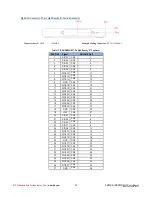
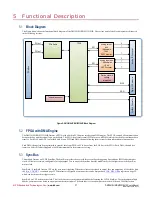
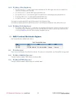
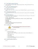
5.7.2
S
IMPLIFIED BLOCK DIAGRAM OF ANALOG OUTPUT
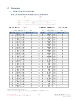
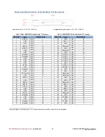
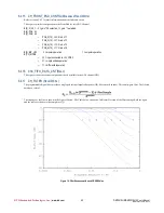
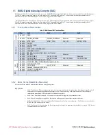
Table 16: DAC Full-Scale Settings
CHn_Front_End_Config
[PGA_A1]
CHn_Front_End_Config
[PGA_A0]
Gain
Bipolar
Mode
0
0
1
±2.5V
0
1
2
±5V
1
0
4
±10V
1
1
8
n/a
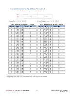
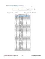
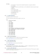
Table 17: Key DAC Bit Weight
DAC Bit Weight
Ideal Output Voltages (mV)
-2.5 to +2.5 V
-5 to +5 V
-10 to +10 V
1111 1111 1111 1111
+2499.9237
+4999.8474
+9999.6948
1000 0000 0000 0001
0.0763
0.1526
0.3052
1000 0000 0000 0000
0.00
0.00
0.00
0111 1111 1111 1111
-0.0763
+0.1526
-0.3052
0000 0000 0000 0000
-2500.00
-5000.00
-10000.00
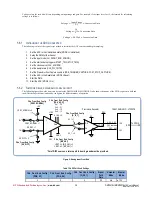
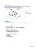
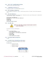
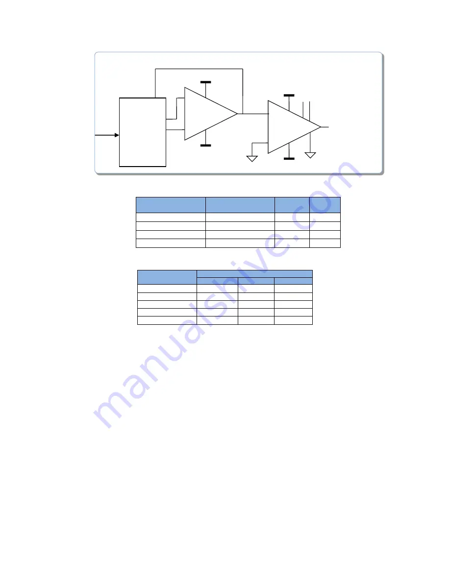
Figure 15: Analog Output
OUT
AD5542A
DIN
-
+
+15V
INV
RFB
+
-
REF
+15V
-15V
-15V
±2.5V
A1 A0
Gain
Analog output
CHn_Front_End_Config
[PGA_A[1:0]]
G=1
:
0, 0
G=2 : 0, 1
G=4 : 1, 0
G=8 : 1, 1


