2 CIRCUIT DESCRIPTION
RT2047 DSC - PART II
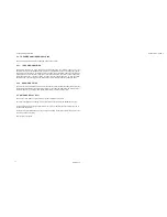
2.6.11 AF CIRCUITS
The AF signal from the receiver is fed to the active filter U5/2-6. The filter provides a frequency response
of -6 dB/Oct. in the range 0.3 to 3 KHz and limits the signals outside this range. Further the signal is fed
to the telephone output amplifier U6/2-6 and Q6-6. From the telephone output the signal is fed through
the VOLUME CONTROL circuit U6-6 and the AL POWER AMP. The DC current in the differential amplifier
in the VOLUME CONTROL is controlled by the transistor between pins 9, 10 and 11. The attenuation will
be minimum when the current through the transistor between pins 3, 4 and 5 is maximum, and this is the
condition when the outputs B1-B4 on the latch U4-6 is high (display reading will be 15). In that case the
voltage on pin 4 of the differential amplifier will be the same as on pin 2. The D/A converter R131-6 to R134-
6 is together with the resistor R128-6 functioning as a voltage divider. With all the outputs B1 - B4 at 0V
the voltage between pin 4 and pin 2 will be approx. 200 Ms. This means that the current through the
transistor between pins 3, 4 and 5 will be minimum and the signal will be attenuated about 60 dB. Resistor
R125-6 and capacitor C58-6 prevents cross talk from the supply voltage to the output of the attenuator.
The AF signal from the receiver is also led through the ‘AF from RX Buffer’ to the Handset Key Connector.
The buffer is a common emitter amplifier with emitter resistance securing a low output impedance and
the signal amplitude required for compatibility with other S.P. RADIO products. This circuit consists of
C77-6 - C79-6, Q19-6 and R157-6 - R162-6. The variable resistor R12-6 is used for adjusting gain and
does in conjunction with C78-6 and R159-6 assure a correct cutoff frequency for the amplifier.
2.6.12 SELCALL
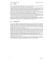
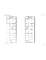
The input to the selcall is taken from the telephone output. The signal is first amplified and limited in U3/
1-6. Then it passes the band pass filter and after this it is rectified and compared with a reference level
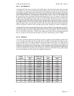
in the comparator U15/1-6. 2.1 MHz is divided in the programmable counter U18-6. The output of this is
divided by 2 and turned into a square wave in the flip-flop U12/1-6. The outputs of the flip-flops are
connected to the switches U13-6. The frequency at which the switches around the capacitors C29-6 and
C30-6 are working determines the resonance frequency of the filter. Thus by changing the dividing figure
to U18-6 it is possible to change the resonance frequency of the filter. With R63-6 it is possible to adjust
the resonance frequency of the filter (see the adjustment procedure).
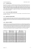
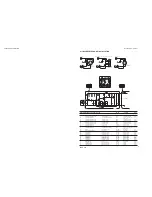
)LJXUH
I
QRPLQDO
,&LQSXW
I
FORFN
I
UHVRQDQFH
QXPEHU
+]
+]
+]
1
1124
1010001
12963
1127
2
1197
1001100
13816
1201
3
1275
1001000
14583
1268
4
1358
1000011
15672
1363
5
1446
0111111
16667
1449
6
1540
0111011
17797
1548
7
1640
0111000
18750
1630
8
1747
0110100
20192
1756
9
1860
0110001
21429
1863
0
1981
0101110
22826
1985
R
2110
0101011
24419
2123
PAGE 2-19
9543
Summary of Contents for RT2047
Page 1: ...S P RADIO A S AALBORG DENMARK TECHNICAL MANUAL FOR COMPACT VHF RT2047 D ...
Page 2: ......
Page 5: ...RT2047 DSC PART I CONTENTS 1 GENERAL INFORMATION 1 1 1 1 INTRODUCTION 1 1 ...
Page 6: ......
Page 8: ......
Page 10: ......
Page 24: ......
Page 30: ...1 GENERAL INFORMATION RT2047 DSC PART II PAGE 1 6 9543 ...
Page 32: ......
Page 34: ......
Page 46: ...2 CIRCUIT DESCRIPTION RT2047 DSC PART II PAGE 2 12 9543 ...
Page 50: ...2 CIRCUIT DESCRIPTION RT2047 DSC PART II 9543 PAGE 2 16 ...
Page 66: ...9546 ...
Page 67: ...2 CIRCUIT DESCRIPTION RT2047 DSC PART II 9546 PAGE 2 33 32162 ...
Page 81: ......
Page 82: ......
Page 84: ......
Page 86: ...3 MECHANICAL DISASSEMBLING AND MODULE LOCATION RT2047 DSC PART II PAGE 3 2 9545 ...
Page 88: ......
Page 90: ......
Page 98: ...4 SERVICE RT2047 DSC PART II PAGE 4 8 9545 ...
Page 99: ...4 SERVICE RT2047 DSC PART II 4 11 PIN CONFIGURATION 9545 PAGE 4 9 ...
Page 109: ...RT2047 DSC PART II CONTENTS 5 PARTS LISTS 5 1 9546 ...
Page 110: ......
Page 124: ......

