background image

8 Troubleshooting

8-6

SAM4S NR-500 SERIES

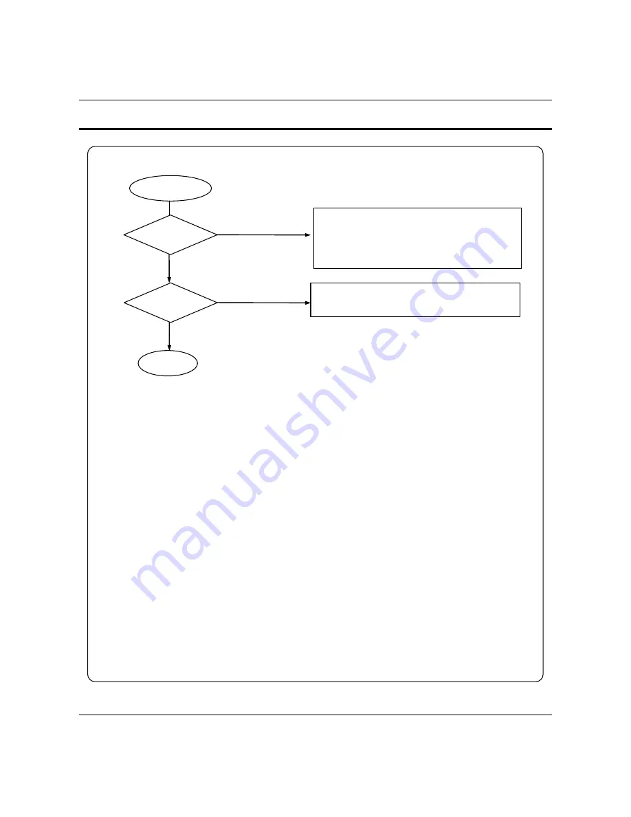
Drawer Problem

Drawer Open

Failure ? 

Y

N

1. Check the Drawer Connector & Harness.

2. Check the VDRW(Drawer Voltage).

3. Check the related circuit & Component TR TIP102(Q3)

4. Check the Harness and Solenoid in the Drawer.

5. Check the Drawer Signal (CPU P8.7)

Compulsory

Failure? 

1. Check the Compulsory Harness & Connector.

2. Check the Micro switch in the Drawer.

N

Y

End

8-6 Drawer Problem


Summary of Contents for NR-500R

Page 1: ...anual 1 Precaution Statements 2 Product Specifications 3 Installation and Operation 4 Disassembly and Assembly 5 Maintenance and Adjustment 6 Exploded Views and Parts List 7 PCB Layout and Parts List...

Page 2: ...Electronic Cash Register Notes Notes may appear anywhere in the manual They describe additional information about the item Precaution symbols Indicates a Safety Precaution that applies to this part co...

Page 3: ...ual may not in whole or in part be copied photocopied reproduced translated or converted to any electronic or machine readable from without prior written permission of Shin Heung Precision Service Man...

Page 4: ...fore you must check the correspondence of your manual with your machine No part of this manual may be copied or reproduced in any form or by any means without the prior written consent of Shin Heung P...

Page 5: ...ges and especially the AC and high voltage supplies Always inspect for pinched out of place or frayed wiring Do not change the spacing between comp onents and the printed circuit board Check the AC po...

Page 6: ...nstrument s ground lead to the instrument chassis ground before connecting the positive lead always remove the instrument s ground lead last 1 3 Precautions for Electrostatic Sensitive Devices ESDs 1...

Page 7: ...al 2 RJ45 Serial 3 RJ45 x Voltage Supply 5V 150mA supplies at 9 Pin of DSUB9 Connector 1 pin RJ45 Connector USB x USB A Type Default Transfer Type BULK Speed 12 Mbps USB 2 0 Full Speed Power Self Powe...

Page 8: ...2 2 A Appearance Dimensions mm Figure2 1 Dimensions 2 2 B Location Feature Figure2 2 Location Feature G Printer Cover G Key Board G Drawer G Customer Display G Operator Display G Mode Key G RS 232 Se...

Page 9: ...tch x 0 0625 mm Maximum Feeding Speed x 75 mm sec At 8 5V of Motor Voltage Power Supply Volt Power Voltage x 4 2 9 5V Recommend TPH Motor Circuit Input Voltage x 3 3V Head Control Sensor Printer Head...

Page 10: ...ji paper Co Ltd F380 Kansaki specialty papers Inc USA 2 3 C Character Specification Item Description Remark Character Structure x 12 W 24 H Font Character Size x 1 25 mm W 3 0 mm H Column Pitch x 1 5...

Page 11: ...D X T 3 R T D 4 G F C N 1 E L A M E F 6 3 D X R 2 G S 5 C N 8 C P N I P 9 E D I S t r o h S n i P 8 6 n i P 7 4 R S D 6 C N 7 D X T 3 R T D 4 E L A M G F C N 1 E L A M D B N O R C E E L A M E F R O T...

Page 12: ...ta to the host or receipt printer after confirming this signal When XON XOFF flow control is selected the printer does not check this signal 9 VCC Output VCC 5V 150mA is supplied at 9 Pin of DSUB9 Con...

Page 13: ...Cable Connection RJ 45 to DSUB 25Pin Caution The VCC is supplied for the barcode or device power source The Supply Current 150mA is total value including Serial 1 and Serial 2 Power Consumption If th...

Page 14: ...er 7 Special Circuit Diagrams 2 5 A h S W Flow Control Timing When XON XOFF flow control is selected the ECR transmits XON ASCII 11h or XOFF ACSII 13h signal through the Serial Data Line If the ECR is...

Page 15: ...2 5 V Differential Receive Sensitivity 200 mV Single End Receive Threshold 0 8 2 5 V Speed 12 Mbps USB 2 0 Full Speed Power Supply Self Power Cable Connector Cable 5m 2m Connector A type Support Spec...

Page 16: ...IN Ethernet Receive Data Line 4 N C 5 N C 6 ENET RX IN Ethernet Receive Data Line 7 N C 8 N C 2 5 C b ETHERNET Interface Cable NR 500 SIDE 1 8 1 8 MAX 100M 5 N C 7 N C 8 N C 4 N C 5 N C 6 ENET RX 7 N...

Page 17: ...t Specification 2 6 A Drawer Signal Description Pin No Signal Name Direction Function 1 S G Signal GND 2 DRAWER OUT Drawer Kick Out Driver Signal 3 DRA_COMP IN Drawer Open Close Signal 4 24V Supply DC...

Page 18: ...2 Product Specifications 2 12 SAM4S NR 500 SERIES MEMO...

Page 19: ...SAM4S NR 500 SERIES 3 1 3 Installation and Operation 3 1 System Configuration Figure 3 1 System Configuration...

Page 20: ...unt of paper as shown Then close the housing cover Fig 3 2 E 6 Passing the leading edge of the paper through the cutter slot Tear off the excess paper Fig 3 2 F 7 In case of 2station feed the leading...

Page 21: ...RS 232C serial Cable to your host computer Figure 3 3 Cable Installation 3 2 C Options No Item Description Remark 1 Water Proof Raised Keyboard Option 2 Memory SRAM 4MBITs 4MBITs 1 On Main PBA Factory...

Page 22: ...ccessible Position Remark VOID VOID OFF Register REG Manager X REG OFF Register REG Z VOID OFF Register REG Manager X Clear Totals Z P VOID OFF Register REG Manager X Clear Totals Z Program PGM C VOID...

Page 23: ...3 Installation and Operation SAM4S NR 500 SERIES 3 5...

Page 24: ...B TOTAL RCPT FEED SERVICE RCPT ON OFF CHECK PLU Figure3 5 Raised Keyboard NR 510R NR 520R 27 45 39 33 3 21 15 9 51 NOSALE 57 26 44 38 32 2 20 14 8 50 RCPT ON OFF 56 28 46 40 34 4 22 16 10 52 52 43 37...

Page 25: ...1 10 12 7 9 6 4 1 3 2 RA CHARGE1 CHECK PO CASH CONV1 SUB TOTAL 51 VOID 57 50 NOSALE 56 52 49 FEED 55 RETURN 58 53 ERROR CORR 59 54 CANCEL 60 8 7 PLU CLEAR RA1 RECEIPT ON OFF 5 4 2 1 00 0 CHARGE1 9 1 X...

Page 26: ...C Key to execute a SERVICE MODE 1 Move to the SERVICE MODE 2 Turn the power switch located on the right side of the register to the OFF position 3 Press and hold the key position where the A CHECK ke...

Page 27: ...prints Figure3 11 All Clear Key Sequence Print Sheet 2014 05 12 MON 09 00 MEMORY ALL CLEAR OK MEMORY ALLOCATION RAM 8Mbits OK RAM 1 OK RAM 2 OK TTLAVAIL 851968 Bytes TTL USED 327850 Bytes VERSION INFO...

Page 28: ...CLEAR key to return to SELF TEST menu 3 3 E d Test Mode Switch 1 From the SELF TEST menu Press 4 to select KEYBOARD 2 From the KEYBOARD menu Press 2 to select MODE KEY TEST 3 Turn the mode switch to a...

Page 29: ...ERFACE menu Press 3 to select USB HOST 4 If USB is OK OK message will be displayed 5 Press the CLEAR key to return to SELF TEST menu Note When the ports is unconnected with the cable the Error occur 3...

Page 30: ...the upper right key and the lower right key A rapid beep beep beep sound will be heard Release the upper right key and the lower right key 11 Press the key and the key to select menu and press the CA...

Page 31: ...Turn the power switch to the OFF position 4 Press the upper right key and the lower right key A rapid beep beep beep sound will be heard Release the upper right key and the lower right key 5 Press th...

Page 32: ...3 Installation and Operation 3 14 SAM4S NR 500 SERIES Perform a memory all clear on the ECR The ECR is now ready to program or to load a previously saved end user program...

Page 33: ...Remove the two screws B29 from the ASS Y CASE UPPER B Page6 3 3 Separate the ASS Y LCD B6 from the ASS Y CASE UPPER B Page6 3 4 Remove the four screws B7 from the ASS Y LCD B6 Page6 3 5 Separate the...

Page 34: ...4 2 B Ass y Main PBA I F PBA 1 Separate the fourteen harnesses and remove the three screws E3 Lift up the PBA MAIN BOARD E4 Page6 13 2 Separate the harness from the PBA I F BOARD E21 Page6 13 3 Lift u...

Page 35: ...hat the thermal head Thermal Element and Radiation Plate becomes very hot during normal operation To prevent the danger of burn injury from thermal be sure to wait for about 10 minutes after turning p...

Page 36: ...5 Maintenance and Adjustment 5 2 SAM4S NR 500 SERIES MEMO...

Page 37: ...SAM4S NR 500 SERIES 6 1 6 Exploded Views and Parts List 6 1 Exploded View NR 520R Figure 6 1 Total Disassembly NR 520R...

Page 38: ...6 Exploded Views and Parts List 6 2 SAM4S NR 500 SERIES 6 1 Exploded View NR 520 Figure 6 2 Total Disassembly NR 520...

Page 39: ...COVER PRINTER NR 510 1 Y IVORY JK95 70675B MEA COVER PRINTER NR 520 1 Y IVORY JK95 70675C MEA COVER PRINTER NR 510B 1 Y BLACK JK95 70675D MEA COVER PRINTER NR 520B 1 Y BLACK A1 JK72 20980A PMO COVER D...

Page 40: ...6 Exploded Views and Parts List 6 4 SAM4S NR 500 SERIES B ASS Y CASE UPPER NR 500R Figure 6 3 ASS Y CASE UPPER NR 500R...

Page 41: ...FRONT 1 Y IVORY JK72 20336D PMO LCD FRONT NR 500B HIPS V0 BLK SPRAY 1 Y BLACK B14 JK72 20825B PMO WINDOW VIEW 1 Y B15 JK72 20891A PMO HOLDER LCD 1 Y IVORY JK72 20891C PMO HOLDER LCD NR 500B HIPS V0 BL...

Page 42: ...6 Exploded Views and Parts List 6 6 SAM4S NR 500 SERIES 6 2 B ASS Y CASE UPPER NR 500 Figure 6 4 ASS Y CASE UPPER NR 500...

Page 43: ...825B PMO WINDOW VIEW 1 Y B15 JK72 20891A PMO HOLDER LCD 1 Y IVORY JK72 20891C PMO HOLDER LCD NR 500B HIPS V0 BLK SPRAY 1 Y BLACK B16 JK72 20349A PMO WINDOW VIEW_R 1 Y B17 JK72 20630A MO WINDOW TURRET...

Page 44: ...6 Exploded Views and Parts List 6 8 SAM4S NR 500 SERIES 6 2 C ASS Y PRINTER Figure 6 5 ASS Y PRINTER...

Page 45: ...1 SII 2 Y C10 JK95 70690A ASSY SPOOL MOTOR 1 Y NR 520 C11 S600200006A SCREW TAPPING PWH M3 L8 2 Y NR 520 C12 JK39 40686C HARNESS SPOOL NR 500 3P 400mm AT TAPE 1 Y C13 S310100012A MOTOR DC 1 Y NR 520 C...

Page 46: ...6 Exploded Views and Parts List SAM4S NR 500 SERIES 6 10 6 2 D ASS Y KBD 48KEY RAISED Figure 6 6 ASS Y KEYBOARD 48 Key...

Page 47: ...D NR 520R RAISED 48KEY 1 Y IVORY JK59 30077D UNIT KEYBOARD NR 520RB RAISED 48KEY 1 Y BLACK D1 JK72 20483A KEY NUMBER SET 1 Y D2 JK72 20476A PMO KEY CAP_1X1 32 Y D3 JK72 20479A PMO KEY TOP_1X1 32 Y D4...

Page 48: ...6 Exploded Views and Parts List SAM4S NR 500 SERIES 6 12 6 2 D ASS Y KBD 90KEY FLAT Figure 6 7 ASS Y KEYBOARD 90 Key...

Page 49: ...esign Location Serviceable Remark D JK59 30027A UNIT KEYBOARD ER 390 90 KEY FLAT 1 Y IVORY JK59 30027B UNIT KEYBOARD ER 390B 90 KEY FLAT 1 Y BLACK D1 JK81 20049A FRAME 90 KEY 1 N D2 JK81 20049B KEY RU...

Page 50: ...6 Exploded Views and Parts List 6 14 SAM4S NR 500 SERIES 6 2 E ASS Y CASE LOWER Figure 6 8 ASS Y CASE LOWER...

Page 51: ...92 01284K PBA SUB FISCAL ER 230 34P 2MBIT 3 3V 1 2Mbit N JK92 10037A PBA SUB FISCAL ER 230 34P 4MBIT 3 3V 1 4Mbit Y E14 S600200028A SCREW TAPPING PWH M3 L6 1 Y E15 S600600005A SCREW ASSY TAPT BH M4 L8...

Page 52: ...30001D POWER CORD NR 500 USA 110V BLACK POWER CORD NR 500 AUSTRALIA 240V BLACK POWER CORD NR 500 UK 240V BLACK USA AUSTRALIA UK E32 JK39 40603A HARNESS DRA COM 4PIN 180mm 1 Y E33 JK92 10139A PBA MICR...

Page 53: ...Parts List SAM4S NR 500 SERIES 6 17 6 2 F ASS Y DRAWER G DRAWER 4B8C 5B6C Figure 6 9 ASS Y DRAWER G DRAWER 4B8C 5B6C A ASS Y BILL COIN 5B6C E ASS Y TRAY B ASS Y HOU SING C ASS Y LOCK D ASS Y BOT TOM A...

Page 54: ...AWER G DRAWER 4B8C 5B6C Figure 6 10 Lubrication Points of the G Drawer 4B8C 5B6C No Code No Description Specification Q ty Serviceable Remark A 0201 002010 GREASE N2 Y Minimum Serviceable Packing Weig...

Page 55: ...R PLATE 5B5C 1 Y a3 JK70 30014A SPRING LEVER PRESS MD 5 Y a4 JK70 30015A SPRING LEVER PRESS PD 5 Y OPTION a5 JK72 20259A PMO LEVER PRESS PLASTIC 5 Y a6 JK70 20067A IPR LEVER PRESS STEEL 5 Y OPTION a7...

Page 56: ...UNV 1 N e1 JK70 60041A RMO RUBBER STOPPER 2 Y e2 JK70 60042A RMO PAD UNIVERSAL 2 Y e3 JK75 20068A MEC ROLLER 2 Y e4 JK70 40302A ICT SHAFT PIN 1 Y e5 JK97 20100A MEA TRAY TILL 1 N e6 6044 000124 RING E...

Page 57: ...6 Exploded Views and Parts List SAM4S NR 500 SERIES 6 21 MEMO...

Page 58: ...SAM4S NR 500 SERIES 7 1 7 PCB Layout and Parts List 7 1 Main PCB Layout...

Page 59: ...BAT43WS BAT54WS 30V 20 D10 D11 D12 D13 D14 D15 D 16 D20 D21 D22 D23 D24 D2 5 D26 D27 D28 D29 D30 D31 D32 Y S0501000279 TR SMALL SIGNAL KSA1182Y PNP 150mW SOT23 10 Q7 Q8 Q11 Q12 Q14 Q15 Q1 6 Q17 Q19 Q2...

Page 60: ...50V 1608 1 C104 N S2204000004 C CERAMIC CHIP 22pF 5 50V 1608 2 C34 C35 N S2204000010 C CERAMIC CHIP 100pF 5 50V 1608 6 C1 C22 C38 C39 C68 C69 N S2204000015 C CERAMIC CHIP 470pF 5 50V 1608 2 C71 C73 N...

Page 61: ...escription Specification Q TY Design Location Serviceable Remarks JK92 10059J PBA PRT JOINT NR 500 SVC 1 ASSY Y S3708001395 CONNECTOR FPC FFC PIC 30P 1mm ST DIP TOP 1 JCN2 Y S3708001397 CONNECTOR FPC...

Page 62: ...17 R CHIP 330 OHM 5 1 10W 1608 1 R5 N S2008000026 R CHIP 1KOHM 1 1 10W 1608 1 5 R1 R10 R11 R14 R15 N S2008000030 R CHIP 2KOHM 5 1 10W 1608 1 R2 N S2008000037 R CHIP 4 7KOHM 1 1 10W 1608 1 4 R8 R9 R12...

Page 63: ...46 00016C UNIT SDHC CARD ER 230EJ 4GB SANDISK MLC CLASS4 1 SD CARD Y SD CARD JK39 40756D HARNESS SD NR 300 ER 230EJ 10P 220mm 1 HARNESS Y JK70 20122A IPR BRKT SD NEX1 SECC T1 0 1 BRACKET Y S2204000004...

Page 64: ...39A PBA MICRO SD NR 300F W O STARCAP 1 MICRO SD B D Y JK39 40756B HARNESS SD ER 230 10P 150mm AT TAPE 1 SCN1 SD HARNESS Y S110900004A UNIT MICRO SD CARD SDHC 4GB SANDISK CLASS4 MLC 1 MICRO SD 4GB Y S3...

Page 65: ...T TAPE 1 HARNESS Y S2204000028 C CERAMIC CHIP 100nF 80 20 25V Y5V 1608 1 C1 N JK41 10574A PCB FISCAL PLCC32 34P FR 4 2L BOARD IN 1 PCB N 7 6 2 Memory Size 4MBITs No Part No Description Specification Q...

Page 66: ...1 U2 Y S2008000044 R CHIP 10KOHM 1 1 10W 1608 1 2 R1 R6 N S2204000028 C CERAMIC CHIP 100nF 80 20 25V Y5V 1608 10 C1 C2 C3 C4 C5 C8 C9 C10 C11 C12 N JK41 10033C PCB INTERFACE JOINT NR 500 3SERIAL FR 4...

Page 67: ...he LM393 U10 2 Check the Power VPRT VDD3 3V 3 Check the related Circuit and Pattern on PCB N N SRAM Ok Y Y N CPU Ok Y N 1 Check the nCS nRD nWR signal of SRAM 2 Check the VBT Battery Voltage 3 Check t...

Page 68: ...the LM393 U10 2 Check the Power VPRT VDD3 3V 3 Check the related Circuit and Pattern on PCB N N SRAM Ok Y Y N CPU Ok Y N 1 Check the nCS nRD nWR signal of SRAM 2 Check the VBT Battery Voltage 3 Check...

Page 69: ...V Ok 1 Refer to the Power Problem 2 Check the Harness LCD PBA Assy Ok Y 1 Check the LCD 2 Check and Replace the LCD MODULE PBA 3 Check the LCD Harness N Y N Back Light OK N Y 1 Check the LCDBL_ONOFF s...

Page 70: ...MOT Feed OK N 1 Check the Phase Signal CPU P5 1 P5 4 P7 4 P8 3 2 Check the Motor Enable Signal CPU P5 5 P8 0 3 Check the motor driver BD6380EFV U12 U16 4 Check the printer FFC harness Replace the pri...

Page 71: ...2 Check the KBD Connector on PBA 3 Check the Key Scan Part 74LVC138 U26 U27 4 Check the Key Return part 74LVC541 U28 5 Check the related Circuit and Pattern Specific Key Failure 1 Check the affected...

Page 72: ...ector Harness 2 Check the VDRW Drawer Voltage 3 Check the related circuit Component TR TIP102 Q3 4 Check the Harness and Solenoid in the Drawer 5 Check the Drawer Signal CPU P8 7 Compulsory Failure 1...

Page 73: ...r 3 Check the TXD RXD DTR DSR Pin on CPU 4 Check the SP3232 Driving Chip and related Circuit on INTERFACE B D Communication Failure 1 Check the connection of the RS 232C and Other side 2 Check the I F...

Page 74: ...8 Troubleshooting 8 8 SAM4S NR 500 SERIES MEMO...

Page 75: ...PIN FFC CABLE PRINTER JOINT BOARD REAR LCD CONTROL FORNT LCD CONTROL DC JACK SERIAL FLASH 1 64Mbit ETHERNET W5100 VPRT 10 PIN HARNESS 10 PIN HARNESS SWITCH GPRS B D SYSTEM CLOCK 12MHZ SERIAL FLASH 2...

Page 76: ...9 Block Diagram 9 2 SAM4S NR 500 SERIES MEMO...

Page 77: ...SAM4S NR 500 SERIES 10 1 10 Wiring Diagram 10 1 Wiring Pin Connection...

Page 78: ...N9 GPRS Board CN13 Fiscal board Connector CN6 Interface Connector 1 DTR 1 EPROM VCC 1 NC 2 RI 2 FISEPROM_PGM 2 NC 3 VPRT 3 GND 3 NC 4 GND 4 FISEPROM_OE 4 NC 5 TRSTN 5 FD 2 5 VSERIAL 5V 6 TDI RXD 6 FD...

Page 79: ...6 2 VAULT_SDA GPRS_TXD 7 RETURN 2 7 SCAN 7 3 VAULT_SCL GPRS_RXD 8 RETURN 1 8 SCAN 8 4 VAULT_SCL GPRS_RXD CN3 Power Switch Connector 9 SCAN 9 5 GND 1 VADAP 9V 10 SCAN 10 6 GND 2 VPRT 11 SCAN 11 7 EXT_R...

Page 80: ...10 Wiring Diagram 10 4 SAM4S NR 500 SERIES MEMO...

Page 81: ...ck 11 6 6 Printer Block 11 7 7 Ethernet Controller Block 11 8 8 Fiscal Logic Block 11 9 9 Fiscal I F Block 11 10 10 Power Power fail Block 11 11 11 Adaptor input VPH Block 11 12 12 Serial Interface Bl...

Page 82: ...wOZPG U GXZUWZUXZ GnwyzGj zSG kSGy k GqT hn G G U GPRS TX RX UART10 GPRS CTS BLCAT PEND CS0 0x600 0000 0x6FF FFFF 0x300 0000 0x3FF FFFF CPU BLOCK LOWBAT_BACKUP TPH_STB_ J R 10K R46 Gwvy GXU GbGl olyul...

Page 83: ...10K _WR _RD CS5_SRAM MEM_CE CS2 File Name 3 CN7 C 2 CN7 B 6 CN7 F 5 CN7 E 9 CN7 I 8 CN7 H R28 300 1K R13 VDD33V D15 BAT43WS R145 1K CS1_SRAM PGM DATA MEMORY 1K R31 VSDCARD1 VSDCARD1 R152 1K MEM BLOCK...

Page 84: ...7 3 CN15 C 5 CN15 E 7 CN15 G File Name VDD33V RETURN 6 RETURN 7 RETURN 3 RETURN 4 RETURN 1 1 CN14 1 CON BOX 8P 2 5MM ST YH 200 R23 VPRT D6 M4 C91 100nF 100nF C89 1 2 BAT1 MS920S FL27E When Power On VB...

Page 85: ...TC 4 GND 1 SC 8 DC 7 SENSE 2 SE KA34063 U5 R60 300 R52 2K SK14 D7 470uF 50V CE6 VDRW 1K R10 R14 10K USB VAULT_SDA GPRS_TXD VAULT_SCL GPRS_RXD EXT_RESET VUSB H W Security Encryption File Name 3 CN2 3...

Page 86: ...on G GwT k G G 2013 07 22 2LINE_REAR_LCD_EN REAR_LCD_RESET 3 CN5 C 2 CN5 B 5 CN5 E 6 CN5 F 2 CN8 B FRONT_LCD_RESET FRONT_GRAP_LCD_EN 4 CN8 D 5 CN8 E 7 CN8 G 8 CN8 H 10 CN8 J VDD33V File Name 2LINE LCD...

Page 87: ...CN12 R 17 CN12 Q 14 CN12 N 15 CN12 O 12 CN12 L 11 CN12 K 9 CN12 I 8 CN12 H 6 CN12 F 5 CN12 E SEN_JTHERMIST_IN 3 CN12 C 2 CN12 B PRINTER_J I F 28 CN11 AB 29 CN11 AC R 25 PG SEN_THERMISTER 26 CN11 Z 25...

Page 88: ...7K 1 GND 3 VDD 2 RST AME8500AEET U11 C54 100nF Shin Heung Precision Co Ltd ETHERNET RESET 77 GNDA 10 GNDA 14 GNDD 13 GNDD 43 GNDD 32 GNDD 12 VCC3V3D 44 VCC3V3D 74 VCC1V8A 33 VCC1V8D 16 VCC1V8D 5 RXIP...

Page 89: ...0 7 Drawn by J Y YUN 4 3 1 R138 10K 100nF C79 100nF C82 12 13 11 U19 D 74LVC32 2 1 3 14 7 U19 A 74LVC32 VDD33V 100nF C80 100nF C94 C97 100pF C99 100pF C101 100pF C95 100pF 8 GND 6 E3 9 Q6 4 E1 11 Q4...

Page 90: ...2222A Q29 R154 10K C84 100nF C85 100nF SK14 D18 10K R139 10K R144 Fiscal EPROM Writing Voltage 12 75V 1 25 1 47K 5 1K FISEPROM_CE Fiscal EPROM VCC 6 2V Fiscal EPROM nCS From CPU File Name FIS_PGM FISE...

Page 91: ...22 H45 NOTE REV0 2 4700uF CAP UGVGyl WUXGwmhpsG ptlG G U 1 G G GY G G GXW G G G UG GXZUWZUW NOTE HEATSINK SIZE UGthpuGw yG G G G G U GXZUW UY VDD33V POWER BLOCK Gz z wmhpsG UG ETHERNET ON OFF I O PORT...

Page 92: ...Date A3 D 2015 10 20 Drawn by J Y YUN 4 3 1 3300uF 16V CE3 2 GND CN1 B File Name ADAPTER 3 GND CN1 C 1K R77 R76 10K R75 47K 4 G 5 D 1 S 2 S 8 D 7 D 3 S 6 D U8 FDS4141 VPH ON OFF VPRT 2 CN3 2 CON BOX...

Page 93: ...rawn by J Y YUN 4 3 1 10K R174 R173 10K VDD33V R55 10K R44 1K SERIAL FLASH HOLD SPI1_CLK SPI1_DI SPI1_DO SPI0_SF_CS1 FLASH MEMORY FISCAL SER 2 CN20 B R119 15K R110 15K R105 33 File Name TXD1 RXD1 RXD0...

Page 94: ...N FISCAL HARNESS 1 29 25 21 33 A4 A7 17 13 9 5 6 D4 D7 VCC VCC 3 1 2 4 C A3 1 A17 A6 A4 GND 30 26 22 34 A16 A2 A0 A14 A0 A3 6 CN3 F 3 CN3 C BLK 5 CN3 E 2 CN3 B A16 A10 A13 D2 D6 D4 18 14 10 A12 A9 A11...

Page 95: ...I 6 CN2 F 3 CN2 C Size NR 500 PRT JOINT sch TITLE D 1 Sheet 1 0 2 GND GND VPH VPH TPH_CLK PEND IN 3 CN1 C 2 CN1 B 6 CN1 F 5 CN1 E 9 CN1 I 8 CN1 H 12 CN1 L 11 CN1 K 15 CN1 O 14 CN1 N 18 CN1 R 17 CN1 Q...

Page 96: ...R5 49 9 VDD33V COM3 VDD33V 100nF C17 VDD33V 12 10 8 7 5 RX TX 1 4 C DTR2_OUT DSR2_IN DTR1_OUT DSR1_IN VSERIAL USB TITLE 8 CN6 H 5 CN6 E 2 CN6 B 8 CN5 H 5 CN5 E 2 CN5 B VUSB D COM3 COM2 COM1 C12 100nF...

Page 97: ...CCDET1 6 CCCLK 4 CCRST 9 CCDET2 12 F G 3 VPP 8 N A 7 N A 11 F G SOCKET SIM CARD 8P CN2 3 VDD 2 RST 1 GND AME8500 U4 10uF 16V CE4 7 BAT_RTC 9 SIM_VCC 1 ADC0 VBATT 3 ADC0 VBATT 5 VCC_1V8 115 RESERVED 1...

Page 98: ...DD33V SD Size Size NR 300 SUB SCH TITLE D D 1 Sheet 1 2 2 2 NO SDC CLK SDC DATA3 GGGGGGGGGG 10 SCN1 J 7 SCN1 G 4 SCN1 D 9 SCN1 I 3 SCN1 C 6 SCN1 F 22pF SC1 GND SD GND SD Date A3 A3 SD CARD B d D D 201...

Page 99: ...3W 10 R3 VDD33V SD CE2 1F 2 5V CE3 1F 2 5V CE1 1F 2 5V Date A3 A3 Date A3 R2 300 VDD33V D D 2014 10 24 D Drawn by Drawn by 4 4 4 3 3 3 1 1 1 1 CN1 A CON BOX 3P 1 25MM ST 12505WS VDD33V 100nF C1 R4 10K...

Page 100: ...D Add JK59 30027B UNIT KEYBOARD ER 390B 90 KEY FLAT 2015 07 21 4th Edition 3 1 Figure 3 1 Before MSR After Pole Display 2016 07 04 5th Edition Many page Interface Board SAECN 15 0071_HW Notification...

Page 101: ......

Page 102: ...Shin Heung Precision Oct 2017 Printed in KOREA V1 6...

Reviews: