6. Schematic Diagrams
6.2. Power
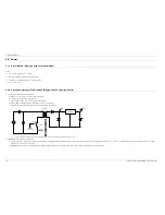
6.2.1. About S.M.P.S (Ringing Choke Converter Method)
Terms
1) 1st : Common power input to 1st winding.
2) 2nd : Circuit followings output winding of transformer.
3) f (Frequency) : Switching frequency (T : Switching cycle)
4) Duty : (Ton/T) x 100
6.2.2. Circuit descripcotion [FLY-Back RCC(Ringing Choke Converter)] Control
1) AC Power Rectification/Smoothing Terminal
a) BD01 ~ 04 : Convert AC power to DC(Wave rectification).
b) C1S05B : Smooth the voltage converted to DC.
c) L1S01, C1S03, C1S04 : Noise removal at power input/output.
d) R1S02 : Rush current limit resistance at the moment of power cord insertion.
Without P1S02, the bridge diode might be damaged as the rush current increases.
2) SNUBBER Circuit : D1S10, C1S10, R1S10
a) Prevent residual high voltage at the terminals of switch during switch off/Suppress noise. High inverted power occurs at switch off, because of the 1st winding of transformer : (V=-L1 xdi/dt. L1 : Leakage Induction) A very high residual voltage exist on both
terminals of IC1 because dt is a very short.
b) SNUBBER circuit protects IC1 from damage through leakage voltage suppression by RC, (Charges the leakage voltage to DIS10 and CIS10 and discharges to R1S10).
6-5
Copyright© 1995-2013 SAMSUNG. All rights reserved.
Summary of Contents for BD-H8500A
Page 19: ...2 Product Specifications Copyright 1995 2013 SAMSUNG All rights reserved 2 11 ...
Page 20: ...2 Product Specifications 2 12 Copyright 1995 2013 SAMSUNG All rights reserved ...
Page 21: ...2 Product Specifications Copyright 1995 2013 SAMSUNG All rights reserved 2 13 ...
Page 22: ...2 Product Specifications 2 14 Copyright 1995 2013 SAMSUNG All rights reserved ...
Page 23: ...2 Product Specifications Copyright 1995 2013 SAMSUNG All rights reserved 2 15 ...
Page 24: ...2 Product Specifications 2 16 Copyright 1995 2013 SAMSUNG All rights reserved ...
Page 25: ...2 Product Specifications Copyright 1995 2013 SAMSUNG All rights reserved 2 17 ...
Page 26: ...2 Product Specifications 2 18 Copyright 1995 2013 SAMSUNG All rights reserved ...
Page 37: ...4 Troubleshooting Copyright 1995 2013 SAMSUNG All rights reserved 4 2 ...
Page 38: ...4 Troubleshooting 4 3 Copyright 1995 2013 SAMSUNG All rights reserved ...
Page 39: ...4 Troubleshooting Copyright 1995 2013 SAMSUNG All rights reserved 4 4 ...
Page 40: ...4 Troubleshooting 4 5 Copyright 1995 2013 SAMSUNG All rights reserved ...
Page 41: ...4 Troubleshooting Copyright 1995 2013 SAMSUNG All rights reserved 4 6 ...
Page 42: ...4 Troubleshooting 4 7 Copyright 1995 2013 SAMSUNG All rights reserved ...
Page 43: ...4 Troubleshooting Copyright 1995 2013 SAMSUNG All rights reserved 4 8 ...
Page 44: ...4 Troubleshooting 4 9 Copyright 1995 2013 SAMSUNG All rights reserved ...
Page 45: ...4 Troubleshooting Copyright 1995 2013 SAMSUNG All rights reserved 4 10 ...
Page 46: ...4 Troubleshooting 4 11 Copyright 1995 2013 SAMSUNG All rights reserved ...
Page 51: ...4 Troubleshooting Copyright 1995 2013 SAMSUNG All rights reserved 4 16 ...
Page 52: ...5 PCB Diagrams 5 PCB Diagrams 5 1 Copyright 1995 2013 SAMSUNG All rights reserved ...
Page 53: ...5 PCB Diagrams 5 1 Wiring Diagram Copyright 1995 2013 SAMSUNG All rights reserved 5 2 ...
Page 54: ...5 PCB Diagrams 5 2 Main PCB 5 3 Copyright 1995 2013 SAMSUNG All rights reserved ...
Page 55: ...5 PCB Diagrams Copyright 1995 2013 SAMSUNG All rights reserved 5 4 ...
Page 56: ...5 PCB Diagrams 5 3 Front PCB 5 5 Copyright 1995 2013 SAMSUNG All rights reserved ...
Page 57: ...5 PCB Diagrams 5 4 Touch PCB Copyright 1995 2013 SAMSUNG All rights reserved 5 6 ...
Page 61: ...6 Schematic Diagrams Copyright 1995 2013 SAMSUNG All rights reserved 6 4 ...
Page 79: ...6 Schematic Diagrams 6 17 CI Main PCB Copyright 1995 2013 SAMSUNG All rights reserved 6 22 ...


