6.
Schematic Diagrams
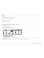
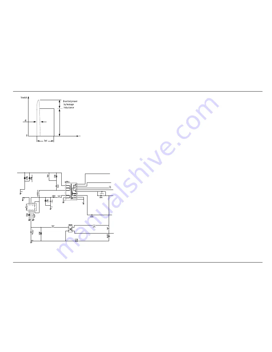
3) IC1S01 Vcc circuit
a) ICIS01, RIS05, RIS07,RIS08 : ICIS01 driving resistance (ICIS01 works through driving resistance at power cord in)
b) ICIS01 Vcc : RIS05, RIS07, RIS08
i) Use the output of transformer as Vcc, because the current starts to flow into transformer while ICIS01 is active
ii) Rectify to DIS07 and smooth to CIS09.
iii) Use the output of transformer as ICIS01 Vcc : The loads are different before and after ICIS01 driving. (Vcc of ICIS01 decreases below OFF voltage , using only the resistance dut to lode increase after ICIS01 driving.)
4) Feedback Control Circuit
a) F/B Terminal of IC1 determines output duty cycle.
b) C-E (Collector-Emitter) of and F/B potential of PQIZ1 are same.
Copyright© 1995-2013 SAMSUNG. All rights reserved.
6-6
Summary of Contents for BD-H8500A
Page 19: ...2 Product Specifications Copyright 1995 2013 SAMSUNG All rights reserved 2 11 ...
Page 20: ...2 Product Specifications 2 12 Copyright 1995 2013 SAMSUNG All rights reserved ...
Page 21: ...2 Product Specifications Copyright 1995 2013 SAMSUNG All rights reserved 2 13 ...
Page 22: ...2 Product Specifications 2 14 Copyright 1995 2013 SAMSUNG All rights reserved ...
Page 23: ...2 Product Specifications Copyright 1995 2013 SAMSUNG All rights reserved 2 15 ...
Page 24: ...2 Product Specifications 2 16 Copyright 1995 2013 SAMSUNG All rights reserved ...
Page 25: ...2 Product Specifications Copyright 1995 2013 SAMSUNG All rights reserved 2 17 ...
Page 26: ...2 Product Specifications 2 18 Copyright 1995 2013 SAMSUNG All rights reserved ...
Page 37: ...4 Troubleshooting Copyright 1995 2013 SAMSUNG All rights reserved 4 2 ...
Page 38: ...4 Troubleshooting 4 3 Copyright 1995 2013 SAMSUNG All rights reserved ...
Page 39: ...4 Troubleshooting Copyright 1995 2013 SAMSUNG All rights reserved 4 4 ...
Page 40: ...4 Troubleshooting 4 5 Copyright 1995 2013 SAMSUNG All rights reserved ...
Page 41: ...4 Troubleshooting Copyright 1995 2013 SAMSUNG All rights reserved 4 6 ...
Page 42: ...4 Troubleshooting 4 7 Copyright 1995 2013 SAMSUNG All rights reserved ...
Page 43: ...4 Troubleshooting Copyright 1995 2013 SAMSUNG All rights reserved 4 8 ...
Page 44: ...4 Troubleshooting 4 9 Copyright 1995 2013 SAMSUNG All rights reserved ...
Page 45: ...4 Troubleshooting Copyright 1995 2013 SAMSUNG All rights reserved 4 10 ...
Page 46: ...4 Troubleshooting 4 11 Copyright 1995 2013 SAMSUNG All rights reserved ...
Page 51: ...4 Troubleshooting Copyright 1995 2013 SAMSUNG All rights reserved 4 16 ...
Page 52: ...5 PCB Diagrams 5 PCB Diagrams 5 1 Copyright 1995 2013 SAMSUNG All rights reserved ...
Page 53: ...5 PCB Diagrams 5 1 Wiring Diagram Copyright 1995 2013 SAMSUNG All rights reserved 5 2 ...
Page 54: ...5 PCB Diagrams 5 2 Main PCB 5 3 Copyright 1995 2013 SAMSUNG All rights reserved ...
Page 55: ...5 PCB Diagrams Copyright 1995 2013 SAMSUNG All rights reserved 5 4 ...
Page 56: ...5 PCB Diagrams 5 3 Front PCB 5 5 Copyright 1995 2013 SAMSUNG All rights reserved ...
Page 57: ...5 PCB Diagrams 5 4 Touch PCB Copyright 1995 2013 SAMSUNG All rights reserved 5 6 ...
Page 61: ...6 Schematic Diagrams Copyright 1995 2013 SAMSUNG All rights reserved 6 4 ...
Page 79: ...6 Schematic Diagrams 6 17 CI Main PCB Copyright 1995 2013 SAMSUNG All rights reserved 6 22 ...


