background image

Samsung Electronics

6-7

PCB Diagrams

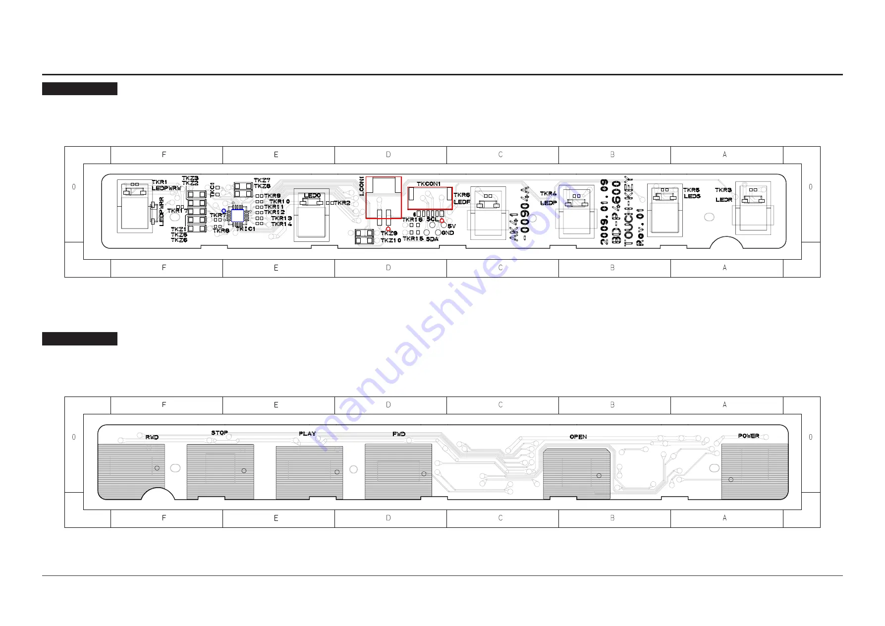
6-4 Touch Key PCB

COMPONENT SIDE

TKIC1

LCON1

TKCON1

CONDUCTOR SIDE

Summary of Contents for BD-P4600

Page 1: ...le International and or domestic law Chassis MONDRIAN BASIC BD P4600 Application Models BD P4600 BD P4610 Application Area XEF XEC XEU XEE XEG EDC XER NWT XSS TSE XTC MEA XFA If you want to know additional information which is not includ ed on this Service Manual Please refer to the SKP Samsung Knowledge Portal web site Area Web Site North America URL http service samsungportal com Latin America U...

Page 2: ... 1 6 10 6 1 Wiring Diagram 6 2 6 2 Main PCB 6 3 6 3 VFD PCB 6 5 6 4 Touch Key PCB 6 7 6 5 USB PCB 6 8 6 6 Remocon PCB 6 9 7 Schematic Diagrams 7 1 7 22 7 1 All block Diagram 7 2 7 2 Ethernet USB S ATA Main PCB 7 3 7 3 VDAC Audio L R SPDIF Main PCB 7 4 7 4 HDMI Main PCB 7 5 7 5 PCI EBI Flash Memory SLC Main PCB 7 6 7 6 Clock BBS Main PCB 7 7 7 7 Power Decoupling Main PCB 7 8 7 8 DDR2 BANK0 Main PCB...

Page 3: ...Samsung Electronics 1 1 Precautions 1 Precautions 1 1 Safety Precautions 1 2 1 2 Servicing Precautions 1 4 1 3 ESD Precautions 1 5 1 4 Handling the optical pick up 1 6 ...

Page 4: ...nt tester or a metering system that complies with American National Standardsp institute ANSI C101 1 Leakage Current for Appliances and Underwriters Laboratories UL 1270 40 7 With the instrument s AC switch first in the ON position and then in the OFF position measure from a known earth ground metal water pipe conduit etc to all exposed metal parts of the instrument antennas handle brackets metal ...

Page 5: ...nched out of place or frayed wiring Do not change spacing between a component and the printed circuit board Check the AC power cord for damage 5 Components parts and or wiring that appear to have overheated or that are otherwise damaged should be replaced with components parts and or wiring that meet original specifications Additionally determine the cause of overheating and or damage and if neces...

Page 6: ...und lead last 2 The service precautions are indicated or printed on the cabinet chassis or components When servicing follow the printed or indicated service precautions and service materials 3 The components used in the unit have a specified flame resistance and dielectric strength When replacing components use components which have the same ratings Components identified by shading by or by in the...

Page 7: ...mbly 3 Use only a grounded tip soldering iron to solder or unsolder ESD devices 4 Use only an anti static solder removal devices Some solder removal devices not classified as anti static can generate electrical charges suffi cient to damage ESD devices 5 Do not use freon propelled chemicals These can generate electrical charges sufficient to damage ESD devices 6 Do not remove a replacement ESD dev...

Page 8: ...your hands on the conductive sheet This gives them the same ground as the sheet 4 Remove the optical pick up block 5 Perform work on top of the conductive sheet Be careful not to let your clothes or any other static sources to touch the unit u Be sure to put on a wrist strap grounded to the sheet u Be sure to lay a conductive sheet made of copper etc Which is grounded to the table 6 Short the shor...

Page 9: ...Samsung Electronics 1 7 Precautions M E M O ...

Page 10: ...Samsung Electronics 2 1 Product Specification 2 Product Specification 2 1 Product Specification 2 2 2 2 Chassis Product Specification 2 7 2 2 Chassis Product Specification 2 8 ...

Page 11: ...e Single Sided Single Layer Disc 135 min CD 5 inches COMPACT DISC Reading Speed 4 8 5 6 m sec Maximum Play Time 74 min CD 3 1 2 inches COMPACT DISC Reading Speed 4 8 5 6 m sec Maximum Play Time 20 min Video Output Composite Video 1 channel 1 0 Vp p 75 Ω load Blu ray DVD Disc 576i 480i Video Audio HDMI 1080p 1080i 720p 576p 480p PCM multichannel audio Bitstream audio Audio Output 2 Channel L 1 L R ...

Page 12: ... to view high definition content The ability to view high definition content on Blu ray Discs may be limited depending on the resolution of your TV q Graphic planes Two individual full HD resolution 1920x1080 video layers are available on top of the HD video layer One layer is assigned to video related graphics like subtitles and the other layer is assigned to interactive elements such as buttons ...

Page 13: ... rst layer to the second layer of a dual layered DVD Video disc there may be momentary distortion in the image and sound This is not a malfunction of the unit Once a DVD RW R recorded in Video Mode is fi nalized it becomes DVD Video Pre recorded prestamped commercial DVDs with movies are also referred to as DVD Videos This unit can play back pre recorded commercial DVD discs DVD Video discs with m...

Page 14: ... q AVCHD Advanced Video Codec High Definition This player can playback AVCHD format discs These discs are normally recorded and used in camcorders The AVCHD format is a high definition digital video camera format The MPEG 4 AVC H 264 format is capable of compressing images at higher efficiency than that of the conventional image compressing format Some AVCHD discs use the x v Color format This pla...

Page 15: ... this Blu ray disc player is described on the bottom panel of the Blu ray disc player BD Region Code Area A North America Central America South America Korea Japan Taiwan Hong Kong and South East Asia B Europe Greenland French territories Middle East Africa Australia and New Zealand C India China Russia Central and South Asia DVD Region Code Area 1 The U S U S territories and Canada 2 Europe Japan...

Page 16: ...it Audio DAC 24bit 192kHz 24bit 192kHz 24bit 192kHz Loader BD ROM O O O BD RE BD R O O O DVD RAM X X X DVD RW O O O DVD ROM O O O DVD R O O O DVD R X X X DVD RW X X X CD ROM O O O CD R O O O CD RW O O O A V Play able Media BD ROM O O O BD RE BD R O O O DVD Video O O O DVD Audio X X X DVD VR X X X Not finalized DVD V Mode X X X VCD 1 1 2 0 X X X SVCD CVD X X X CD DA O O O DTS CD O O O HDCD X X X SA...

Page 17: ... XEF S N A Composite Video Audio L R Cable AC39 00073A Model Standard of BD P4600 XEF Adapter BN44 00139A Model Standard of BD P4600 XEF Adapter Cable 3903 000085 Model Standard of BD P4600 XEF Assy Stand AK97 02476A Model Standard of BD P4600 XEF Assy Bracket wall AK97 02475A Model Standard of BD P4600 XEF COVER JACK AK96 01144A Model Standard of BD P4600 XEF A B 0 1 2 3 7 8 9 4 5 6 RET URN POWER...

Page 18: ...Samsung Electronics 2 9 Product Specification M E M O ...

Page 19: ...Samsung Electronics 3 1 Disassembly and Reassembly 3 Disassembly and Reassembly 3 1 Cabinet and PCB 3 2 3 2 PCB Location 3 8 3 3 Deck 3 9 ...

Page 20: ...B Samsung Electronics 3 2 3 1 1 Cover Top Removal 1 Remove 6 Screws q 2 Lift up the Cover Top w in direction of arrow 3 Disconnect FFC e form CON4 on the VFD PCB Fig 3 1 Cover Top Removal w COVER TOP e FFC CON4 CAUTION Connector Must be remove with care q 6 SCREWS 3X10 B ...

Page 21: ...Samsung Electronics 3 3 Disassembly and Reassembly 3 1 2 Top Cabinet Removal 1 Release 2 Hooks q 2 Remove Top Cabinet w and lift it up Fig 3 2 Top Cabinet Removal w TOP CABINET q 2 HOOKS ...

Page 22: ...lectronics 3 1 3 VFD PCB and RMC PCB Removal 1 Disconnect FFC q form FCON1 on the Main PCB 2 Remove 1 Screw w from the VFD PCB and RMC PCB e r and lift it up Fig 3 3 VFD PCB and RMC PCB Removal w 1 SCREW 3X10 B e VFD PCB q FFC FCON1 r RMC PCB ...

Page 23: ...C w form CON17 CON5 on the Main PCB 2 Remove 2 Screws e from the Ass y Deck r and lift it up 3 Remove 3 Screws t y u from the Bracket Deck i and lift it up Fig 3 4 Ass y Deck and Bottom Cabinet Removal e 2 SCREWS 3X10 B r ASS Y DECK i BRACKET DECK q FFC w FFC CON5 CON17 t 1 SCREW M 2X4 u 1 SCREW M 2X4 y 1 SCREW M 2X4 ...

Page 24: ... PCB Removal 1 Disconnect Cable q form UCON1 on the Main PCB 2 Remove 3 Screws w from the Main PCB e and lift it up 3 Remove 1 Screw r from the USB PCB t and lift it up Fig 3 5 Main PCB and USB PCB Removal e MAIN PCB q CABLE UCON1 t USB PCB r 1 SCREW 3X10 B w 3 SCREWS 3X6 W ...

Page 25: ...ssembly and Reassembly 3 1 6 Bottom Cabinet and FAN Removal 1 Remove Bottom Cabinet q and lift it up 2 Remove 2 Screws w from the FAN e and lift it up Fig 3 6 Bottom Cabinet and FAN Removal q BOTTOM CABINET e FAN w 2 SCREWS M 3X10 ...

Page 26: ...Disassembly and Reassembly 3 8 Samsung Electronics 3 2 PCB Location Fig 3 7 PCB Location MAIN PCB USB PCB VFD PCB ...

Page 27: ...ck 3 3 1 FFC Pick up Removal 1 Take off FFC Pick up q from the Bracket FFC e 2 Remove the 2 Screws w 3 Remove the Bracket FFC e Fig 3 8 FFC Pick up Removal q FFC PICK UP 40PIN w 2 SCREWS 1 7X4 e BRACKET FFC Initial FFC Pick up Assemble State View BOTTOM VIEW ...

Page 28: ...nnector pin 4 w 2 Disconnect Feeding Motor FPC e from Connector pin 4 r 3 Remove the 3 Screws t 4 Lift up the Ass y Traverse Deck y 5 Remove the FFC Deck u Fig 3 9 Ass y Traverse Deck Removal r CONNECTOR 4PIN u FFC DECK 14PIN w CONNECTOR 4PIN t 3 SCREWS 2x5 y ASS Y TRAVERSE DECK q SPINDLE MOTOR FFC e FEEDING MOTOR FPC BOTTOM VIEW ...

Page 29: ...ve 3 Pull the FFC Connrctor Cover u in the direction of arrow B and disconnect FFC Pick up i 4 Remove the 1 Screw o and Ass y Hinge PU a Fig 3 10 Ass y Pick up Removal i FFC PICK UP u FFC CONNECTOR COVER a ASS Y HINGE PU o 1 SCREW 1 4x3 q 1 SCREW 2X7 t ASS Y PICK UP r SHAFT MAIN w COVER SKEW A e SPRING SKEW y HOLDER SHAFT MAIN BOTTOM VIEW A B NOTICE Spring Skew e is easy to lose Please keep carefu...

Page 30: ...ft Main t 4 Hole of Ass y Pick up y insert to Shaft Main q 5 Another end of Shaft Main q Assemble Holder Shaft Main t 6 When work above issue Gear teeth of Assy Hinge PU i engage with Lead Screw of Feeding Motor o Fig 3 11 Reassemble Ass y Pick up r SPRING SKEW t HOLDER SHAFT MAIN o FEEDING MOTOR i ASS Y HINGE PU e PLATE SPRING SKEW q SHAFT MAIN 1 SCREW 1 SCREW COVER SKEW A q SHAFT MAIN y ASS Y PI...

Page 31: ...Samsung Electronics 3 13 Disassembly and Reassembly M E M O ...

Page 32: ...Samsung Electronics 4 1 4 Trouble Shooting 4 1 Trouble Shooting 4 2 4 2 Adjustment 4 15 4 3 Software Update 4 18 ...

Page 33: ...FF PJACK2 PIN1 is normal Voltage Level 12V PWF1 voltage is normal Voltage Level 12V Is the FFC cable between SUB PCB Main PCB OK FCON1 pin9 is normal Voltage Level 5V CHANGE THE SUB PCB Change Adaptor Change FUSE PWF1 Re insert FFC cable correctly CHANGE THE MAIN PCB No Yes No No No Yes Yes Yes ...

Page 34: ... Check Current Digital Audio Setting is PCM Set to Bitstream No Yes Check the A V Receiver can Decode Current Bit Steam No Yes Check the jack soldering or replace Optical jack Check the Audio Data at R125 No Yes Replace the Main PCB Refer to a pattern image of Table 4 1 ...

Page 35: ...Trouble Shooting 4 4 Samsung Electronics Fig 4 1 PIC6 AIC1 Refer to a pattern image of Main PCB page 6 3 q DIGITAL AUDIO DATA R125 Refer to a pattern image of VDAC Audio L R SPDIF Main PCB Page 7 4 ...

Page 36: ... 7 6 of AIC1 PIN1 2 23 Clock data PIN6 Audio data Check the Audio signal at PIN 13 15 of AIC1 Check the Audio signal at AIC1 Audio cable error Replace the main PCB Check AIC1 soldering or replace AIC1 Check AIC1 soldering of peripheral device No Yes No No Yes Yes Refer to a pattern image of Table 4 2 ...

Page 37: ...Trouble Shooting 4 6 Samsung Electronics Fig 4 3 AIC1 Refer to a pattern image of Main PCB page 6 3 q ANALOG AUDIO DATA AIC1 Refer to a pattern image of VDAC Audio L R SPDIF Main PCB Page 7 4 ...

Page 38: ...c Ioading error Check the deck power at CON5 CON17 8VA 5VA Is the DECK cable between main deck inserted correctly Check the clock at X1 25MHz Change the deck Check the power Reinsert DECK Cable correctly Change the Main board No Yes No No Yes Yes ...

Page 39: ...ol does not work Remocon battery OK Is the FFC cable between SUB PCB Main PCB OK IR1 PIN1 SIGNAL OK Check the Power of FMIC1 PIN47 or change the Main PCB Change the battery Re insert FFC cable correctly Check IR1 or change the SUB PCB No Yes No No Yes Yes ...

Page 40: ...Samsung Electronics 4 9 Trouble Shooting No Picture Logo screen is OK NO LOGO HDMI No Yes HDMI No Yes BD DVD Playback is OK No Yes CHANGE THE MAIN PCB NO LOGO CVBS ...

Page 41: ...th cable connection and TV mode Video output from JACK1 R79 Video output from VIC1 VC1 CVBS cable error Check the Video select cable connection TV mode JACK1 R79 soldering error Check VIC1 soldering of peripheral devices Input power level is normal 3 3V on pin 6 No Yes No No Yes Yes ...

Page 42: ...happen with only specific Blu ray Disc title Is the firmware of the Unit is older version than the latest firmware which is available on the Sam sung Web Site Update with the new version and try again Refef to Disc Loading Error Consuit with the Samsung Electronics No Yes No Yes ...

Page 43: ...voltage at CON5 TP name LTHR 0V 1V RFIP Check Signal level OK BDROM SL over 300mV DVDROM SL over 400mV CDROM SL over 400mV Only BD NG Only DVD NG Only CD NG Change the Main Board Change the Main Board Change the Main Board SMPS Check Change the DECK Change the DECK Yes Yes Yes Yes No No No No Yes Yes Yes Yes No No No Refer to a pattern image of Table 4 3 Refer to a pattern image of Table 4 4 ...

Page 44: ...Samsung Electronics 4 13 Trouble Shooting Fig 4 3 CON5 Refer to a pattern image of Main PCB page 6 3 q LTHR 0V 1V Refer to a pattern image of BCM7620 F E Main PCB Page 7 15 ...

Page 45: ... 14 Samsung Electronics Fig 4 4 FEU2 FEU3 Refer to a pattern image of Main PCB page 6 4 q RFIP Check BDROM SL over 300mV DVDROM SL over 400mV CDROM SL over 400mV Refer to a pattern image of BCM7620 F E Main PCB Page 7 15 ...

Page 46: ...ng remote control It means adjustment of the touch key s sensitivity to optimize in the current environment q METHOD Step 1 Open tray mode Step 2 Press number 86824 using remote control Step 3 Verify the message on front display then automatically close tray Step 4 Press the ENTER button then complete Fig 4 5 Fig 4 6 4 2 Adjustment ...

Page 47: ...n to reset pick up condition through auto adjustment of loader q Method Step 1 No disc mode Step 2 Press number 235878 using remote control Step 3 Verify the message Adjusting on screen Step 4 Open tray And then insert single sided Blu ray Disc Step 5 After playback insert single sided DVD disc Step 6 Eject disc after playback then complete Fig 4 7 Fig 4 8 ...

Page 48: ...te control And then you can see this message Fig 4 9 adjustment result OK is complete normally NG is NOT complete or Failed or No Data BD collimator value BD tilt value DVD tilt value error code during adjustment Fig 4 10 This is useful for forgotten Parental Lock password Press vv on the front panel for over 5 seconds while no disc status Then VFD sign RESET ...

Page 49: ...compressed zip or rar the file should be uncompressed to CD image file iso q Network Update q The method of USB Update and CD Update is very similar u F W Update Method by USB flash drive q How to prepare F W Update file via USB flash drive Download the newest firmware file onto your computer from www samsung com If the firmware file is compressed zip the file should be uncompressed to RUF file ru...

Page 50: ...anel Press Yes if the USB you inserted has a later one than Current Version Remove the USB flash drive Wait about 2 3 minutes When finished the power will turn off automatically Wait about 2 3 minutes When Finished power automatically goes off Fig 4 15 Fig 4 16 Fig 4 13 Fig 4 17 Fig 4 14 XEF XEF XEF XEF ...

Page 51: ...firmware file is compressed zip the file should be uncompressed to CD image file iso Please burn the CD image file on a blank CD R RW disc Recommended CD Burning Program is Nero Burning ROM q Warning The following events may interrupt the upgrade process and MAY RESULT IN PERMANENT DAMAGE TO THE UNIT WHILE UPGRADING Unplugging the power plug Power Outage Dirt or Scratches on the burned CD R RW dis...

Page 52: ... If no latest version is released the latest version has been already installed The latest version of the fi rmware is already installed There is no need to update If there is a disc in the player Please maintain No Disc state for network update This indicates that you must remove all discs from the unit to perform the update If the server service is not available Update Server is under maintenanc...

Page 53: ... Display Setup HDMI Setup Network Setup Parental Setup Music Photo Setup Touch Key Sound On BD Data Management DivX R Registration System Update System Update Verifying update data Please wait 1 2 3 4 No Disc System Setup Language Setup Audio Setup Display Setup HDMI Setup Network Setup Parental Setup Music Photo Setup Touch Key Sound On BD Data Management DivX R Registration System Update System ...

Page 54: ...Samsung Electronics 4 23 Trouble Shooting M E M O ...

Page 55: ...5 Exploded View and Parts List Samsung Electronics 5 1 5 1 Cabinet Assembly 5 2 5 2 Deck Parts 5 4 5 3 Electrical Parts List 5 6 ...

Page 56: ...KET DECK S N A TOUCH KEY PCB S N A A001 M0158 T0268 P148 W001 W001 W001 W001 W001 W275 T0265 CON4 P112 CON2 M0081 M0081 M0081 M0541 M0019 UCN1 ASSY DECK S N A FOOT BOTTOM S N A FOOT BOTTOM S N A A B 0 1 2 3 7 8 9 4 5 6 RETURN POWER EJECT AUDIO SUBTITLE REPEAT REPEAT CANCEL TV SOURCE STOP PLAY BONUSVIEW PAUSE TV MUTE ENTER POPUP MENU DISC MENU TITLE MENU A B C D M E N U E X IT IN FO TVVOL TV CH TV ...

Page 57: ...K92 01809A ASSY PCB USB BD P4600 XAA ASSY PC 1 SA M0081 6003 001070 SCREW TAPTYPE BH B M2 L4 ZPC BLK 4 SA M0158 BN44 00139A ADAPTOR SAD03612A UV ADAPTOR 90 2 1 SA M0541 AK92 01879A ASSY PCB RMC BD P4600 XAA ASSY PC 1 SA P030 3103 001207 FAN DC 12VDC 40mA 3000rpm 0 065m 3 1 SA P112 AK92 01808A ASSY PCB VFD BD P4600 XAA ASSY PC 1 SA P148 AK97 02476A ASSY STAND BD PLAYER BD P4600 XAA 1 SA T0265 AK97 ...

Page 58: ...Document can not be used without Samsung s authorization Samsung Electronics 5 2 Deck Parts W101 2 X 5 SCREW W104 2 X 7 SCREW W102 1 4 X 3 SCREW W100 1 7 X 4 SCREW T100 T102 T101 T200 H100 H200 14PIN 40PIN PICKUP H201 H101 COVER SKEW A S N A ...

Page 59: ... FFC PICK UP BD S4 PET 40P T0 08 L25 1 SA PICKUP AK96 01017A ASSY PICK UP SOH SBP1 BD SLIM PICKU 1 SA T100 AK96 01011A ASSY TRAVERSE DECK BD S4 1 SA T101 AK61 00919A SPRING ETC SKEW BD S4 SWPB PI0 23 O 4 SA T102 AK66 00153A SHAFT MAIN BD S4 SUS303N OD3 0 NTR 1 SA T200 AK96 01033A ASSY HINGE PU BD S4 POM SUS304 1 SA W100 6003 001527 SCREW TAPTYPE BH B M1 7 L4 ZPC BL 2 SA W101 6003 001742 SCREW TAPT...

Page 60: ... C CER CHIP 100nF 10 10V X7R 1005 1 SA C128 2203 006048 C CER CHIP 100nF 10 10V X7R 1005 1 SA C129 2203 006048 C CER CHIP 100nF 10 10V X7R 1005 1 SA C131 2203 006048 C CER CHIP 100nF 10 10V X7R 1005 1 SA C132 2203 000812 C CER CHIP 033nF 5 50V C0G 1005 1 SNA C133 2203 000812 C CER CHIP 033nF 5 50V C0G 1005 1 SNA C134 2203 006048 C CER CHIP 100nF 10 10V X7R 1005 1 SA C136 2203 000254 C CER CHIP 10n...

Page 61: ... 2203 006361 C CER CHIP 10000nF 10 10V X5R TP 2 1 SC FEC100 2203 006048 C CER CHIP 100nF 10 10V X7R 1005 1 SA FEC101 2203 006048 C CER CHIP 100nF 10 10V X7R 1005 1 SA FEC102 2203 006698 C CER CHIP 1000nF 10 25V X7R 1608 1 SNA FEC103 2203 006048 C CER CHIP 100nF 10 10V X7R 1005 1 SA FEC104 2203 006048 C CER CHIP 100nF 10 10V X7R 1005 1 SA FEC105 2203 006048 C CER CHIP 100nF 10 10V X7R 1005 1 SA FEC...

Page 62: ...7Kohm 5 1 16W TP 1005 1 SNA FER127 2007 000148 R CHIP 10Kohm 5 1 16W TP 1005 1 SA FER129 2007 000157 R CHIP 47Kohm 5 1 16W TP 1005 1 SNA FER130 2007 000152 R CHIP 20Kohm 5 1 16W TP 1005 1 SNA FER131 2007 000148 R CHIP 10Kohm 5 1 16W TP 1005 1 SA FER132 2007 000155 R CHIP 27Kohm 5 1 16W TP 1005 1 SNA FER133 2007 000155 R CHIP 27Kohm 5 1 16W TP 1005 1 SNA FER139 2007 000341 R CHIP 120Kohm 5 1 4W TP ...

Page 63: ...P 1005 1 SNA HR7 2007 000171 R CHIP 0ohm 5 1 16W TP 1005 1 SNA HR8 2007 000171 R CHIP 0ohm 5 1 16W TP 1005 1 SNA HR9 2007 000171 R CHIP 0ohm 5 1 16W TP 1005 1 SNA HUC1 2203 006158 C CER CHIP 100nF 10 16V X7R 1005 1 SA HUC10 2203 000552 C CER CHIP 0 02nF 5 50V C0G 1608 1 SNA HUC11 2203 005065 C CER CHIP 1000nF 80 20 10V Y5V 1 1 SNA HUC12 2203 006158 C CER CHIP 100nF 10 16V X7R 1005 1 SA HUC13 2203 ...

Page 64: ...10 16V X7R TP 160 1 SNA PWC39 2203 005148 C CER CHIP 100nF 10 16V X7R TP 160 1 SNA PWC4 2203 000476 C CER CHIP 1000nF 80 20 16V Y5V 2 1 SA PWC41 2203 006474 C CER CHIP 22000nF 20 6 3V X5R 201 1 SA PWC43 2203 006474 C CER CHIP 22000nF 20 6 3V X5R 201 1 SA PWC44 2203 006474 C CER CHIP 22000nF 20 6 3V X5R 201 1 SA PWC5 2203 006361 C CER CHIP 10000nF 10 10V X5R TP 2 1 SC PWC51 2203 006158 C CER CHIP 1...

Page 65: ...0 1 SNA VIC1 1201 002800 IC VIDEO AMP MM1756AURE TSOP 6P 2x1 1 SNA VR1 2007 008015 R CHIP 75ohm 1 1 16W TP 1005 1 SNA VR2 2007 008015 R CHIP 75ohm 1 1 16W TP 1005 1 SNA VR3 2007 000171 R CHIP 0ohm 5 1 16W TP 1005 1 SNA X TAL2 2801 004008 CRYSTAL SMD 24MHz 20ppm 28 AAN 12pF 1 SA Y1 2801 004284 CRYSTAL SMD 27MHZ 10PPM 28 AAN 20PF 1 SA AK99 02191A ASSY MANUAL INSERT BD PLAYER BD P46 1 SNA 0202 001463...

Page 66: ...ohm 5 1 16W TP 1005 1 SNA TKR11 2007 000139 R CHIP 220ohm 5 1 16W TP 1005 1 SNA TKR12 2007 000139 R CHIP 220ohm 5 1 16W TP 1005 1 SNA TKR13 2007 000139 R CHIP 220ohm 5 1 16W TP 1005 1 SNA TKR14 2007 000138 R CHIP 100ohm 5 1 16W TP 1005 1 SNA TKR15 2007 000070 R CHIP 0ohm 5 1 10W TP 1608 1 SNA TKR17 2007 001311 R CHIP 270ohm 5 1 16W TP 1005 1 SA TKR2 2007 001311 R CHIP 270ohm 5 1 16W TP 1005 1 SA T...

Page 67: ...1819 ADHESIVE UV 8833M YELLOW 21000mPas 0 05 SNA AK68 01760A LABEL STICKER SOH BP5 0 1 10 15 WHI 1 SNA AK96 01019A ASSY SUB PICK UP SOH SBP1 BD SLIM P 1 SNA 0201 001525 ADHESIVE UV 8840L YEL TRANS 23000 D 0 00004 SNA 0201 001709 ADHESIVE UV 8839L YEL 24500mPa s 0 00001 SNA 0201 001819 ADHESIVE UV 8833M YELLOW 21000mPas 0 02 SNA 0202 001499 SOLDER WIRE FLUX SR34 SUPER LFM 48 0 05 SNA 0602 001158 DI...

Page 68: ... CONNECTOR FPC FFC PIC 40P 0 5mm SMD 1 SNA AK41 00895A FPC MAIN SOH SBP1 1 4 PCB 40 T0 3 1 SNA AK31 00040A MOTOR DC LOADING BD S4 1 SNA AK66 00135A PULLEY MOTOR BD S4 POM NTR 1 SNA 3409 001194 SWITCH DETECTOR 5V 0 1mA 100mA 28 3 SNA C A V AC39 42001R CABLE A V PVC 1 SA M0081 6003 001070 SCREW TAPTYPE BH B M2 L4 ZPC BLK 3 SA T0153 AK69 00702C PACKING CASE BD P4600 CB SW2 A 1 TY 1 SA T0511 AK68 0180...

Page 69: ...Exploded Views and Parts List 5 15 This Document can not be used without Samsung s authorization Samsung Electronics Samsung Electronics 5 15 M E M O ...

Page 70: ...6 PCB Diagrams 6 1 Wiring Diagram 6 2 6 2 Main PCB 6 3 6 3 VFD PCB 6 5 6 4 Touch Key PCB 6 7 6 5 USB PCB 6 8 6 6 Remocon PCB 6 9 Samsung Electronics 6 1 ...

Page 71: ...6 2 Samsung Electronics PCB Diagrams 6 1 Wiring Diagram ...

Page 72: ... NAND1 UIC1 UCON1 OPUCN1 FCON1 FANCN CON5 CON17 COMPONENT SIDE LOC NO X Y OPUCN1 A 0 UIC1 A 2 UCON1 A 2 FCON1 B 0 FANCN B 0 CON5 C 0 FMIC1 C 0 FU2 C 1 NAND1 C 1 IC1 C 1 PIC5 C 2 OPSCN2 C 2 VIC1 C 3 CON17 D 0 FEIC13 D 1 CON16 D 1 OPSCN1 D 2 PIC6 D 2 CON15 E 1 FEU5 E 2 PIC4 E 2 q DIGITAL AUDIO DATA R125 w ANALOG AUDIO DATA AIC1 ...

Page 73: ...Electronics PCB Diagrams IC2 NAND2 NAIC1 FU1 FU3 FU4 PIC2 FEU1 PIC1 PIC3 FEU2 FEU3 CONDUCTOR SIDE LOC NO X Y FEU2 A 0 FEU1 A 1 PIC3 A 2 FEU3 B 0 PIC1 B 2 PIC2 B 2 FU1 C 0 FU3 C 0 FU4 C 0 NAIC1 C 1 NAND2 C 1 IC2 E 2 ...

Page 74: ...Samsung Electronics 6 5 PCB Diagrams 6 3 VFD PCB CON4 CON2 COMPONENT SIDE ...

Page 75: ...6 6 Samsung Electronics PCB Diagrams VFD2 CONDUCTOR SIDE ...

Page 76: ...Samsung Electronics 6 7 PCB Diagrams 6 4 Touch Key PCB COMPONENT SIDE TKIC1 LCON1 TKCON1 CONDUCTOR SIDE ...

Page 77: ...6 8 Samsung Electronics PCB Diagrams 6 5 USB PCB COMPONENT SIDE CONDUCTOR SIDE ...

Page 78: ...Samsung Electronics 6 9 PCB Diagrams 6 6 Remocon PCB COMPONENT SIDE CONDUCTOR SIDE ...

Page 79: ...6 10 Samsung Electronics PCB Diagrams M E M O ...

Page 80: ...sh Memory Local Storage Main PCB 7 17 7 17 Remocon Remocon PCB 7 18 7 18 Touch Key Touch PCB 7 19 7 19 USB USB PCB 7 20 7 20 VFD BLCOK VFD PCB 7 21 For schematic Diagram Resistors are in ohms 1 8W unless otherwise noted Note Do not use the part number shown on this drawing for ordering The correct part number is shown in the parts list may be slightly different or amended since this drawing was pr...

Page 81: ...7 2 This Document can not be used without Samsung s authorization Samsung Electronics Schematic Diagrams 7 1 All block Diagram Video Audio ...

Page 82: ...Schematic Diagrams Samsung Electronics This Document can not be used without Samsung s authorization 7 3 7 2 Ethernet USB S ATA Main PCB Power ...

Page 83: ...zation Samsung Electronics Schematic Diagrams 7 3 VDAC Audio L R SPDIF Main PCB Power Audio Video q DIGITAL AUDIO DATA R125 w ANALOG AUDIO DATA AIC1 u These are the waveforms of BD P4600 Caution There can be some differences Voltage Frequency stc among cameras ...

Page 84: ...Schematic Diagrams Samsung Electronics This Document can not be used without Samsung s authorization 7 5 7 4 HDMI Main PCB Power Video ...

Page 85: ...7 6 This Document can not be used without Samsung s authorization Samsung Electronics Schematic Diagrams 7 5 PCI EBI Flash Memory SLC Main PCB Power ...

Page 86: ...Schematic Diagrams Samsung Electronics This Document can not be used without Samsung s authorization 7 7 7 6 Clock BBS Main PCB Power ...

Page 87: ...7 8 This Document can not be used without Samsung s authorization Samsung Electronics Schematic Diagrams 7 7 Power Decoupling Main PCB Power ...

Page 88: ...Schematic Diagrams Samsung Electronics This Document can not be used without Samsung s authorization 7 9 7 8 DDR2 BANK0 Main PCB Power ...

Page 89: ...7 10 This Document can not be used without Samsung s authorization Samsung Electronics Schematic Diagrams 7 9 DDR2 BANK1 Main PCB Power ...

Page 90: ...Schematic Diagrams Samsung Electronics This Document can not be used without Samsung s authorization 7 11 7 10 Boot Strap Option Main PCB Power ...

Page 91: ...7 12 This Document can not be used without Samsung s authorization Samsung Electronics Schematic Diagrams 7 11 GPIO Block Reset Main PCB Power ...

Page 92: ...Schematic Diagrams Samsung Electronics This Document can not be used without Samsung s authorization 7 13 7 12 Front Micom Main PCB Power ...

Page 93: ...7 14 This Document can not be used without Samsung s authorization Samsung Electronics Schematic Diagrams 7 13 Main Power Main PCB Power ...

Page 94: ...Schematic Diagrams Samsung Electronics This Document can not be used without Samsung s authorization 7 15 7 14 BCM7620 F E Main PCB ...

Page 95: ...7 16 This Document can not be used without Samsung s authorization Samsung Electronics Schematic Diagrams 7 15 USB Hub IC Main PCB Power ...

Page 96: ...Schematic Diagrams Samsung Electronics This Document can not be used without Samsung s authorization 7 17 7 16 Flash Memory Local Storage Main PCB Power ...

Page 97: ...7 18 This Document can not be used without Samsung s authorization Samsung Electronics Schematic Diagrams 7 17 Remocon Remocon PCB Power ...

Page 98: ...K KEY_SCL TKR7 220 TKZ5 1N4148WS 5V GND PLAY TKZ3 1N4148WS SCL TKR8 220 STOP TKR9 220 TKR2 1K KEY_SDA TKR12 220 TKZ9 1N4148WS GND TKR15 0 TKR17 1K TKIC1 TC10QF20IF 1 RESETB ADCH0 P1 2 2 TS7 T0 ADCH2 P2 0 3 TS6 T1 ADCH3 P2 1 4 TS5 ADC11 P2 2 5 TS4 ADC10 P2 3 6 ADC9 P2 4 7 ADC8 P2 5 8 CLO ADC7 P2 6 9 ADC6 P0 7 10 ADC6 P0 6 11 P0 5 ADC4 SCL0 12 P0 4 ADC3 SDA0 13 P0 3 ADC2 INT3 TS3 14 P0 2 ADC1 INT2 T...

Page 99: ...7 20 This Document can not be used without Samsung s authorization Samsung Electronics Schematic Diagrams 7 19 USB USB PCB Power ...

Page 100: ...Schematic Diagrams Samsung Electronics This Document can not be used without Samsung s authorization 7 21 7 20 VFD BLCOK VFD PCB Power ...

Page 101: ...7 22 Samsung Electronics Schematic Diagrams M E M O ...

Reviews: