KS57C2308/P2308/C2316/P2316
POWER-DOWN
8-7
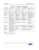
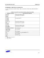
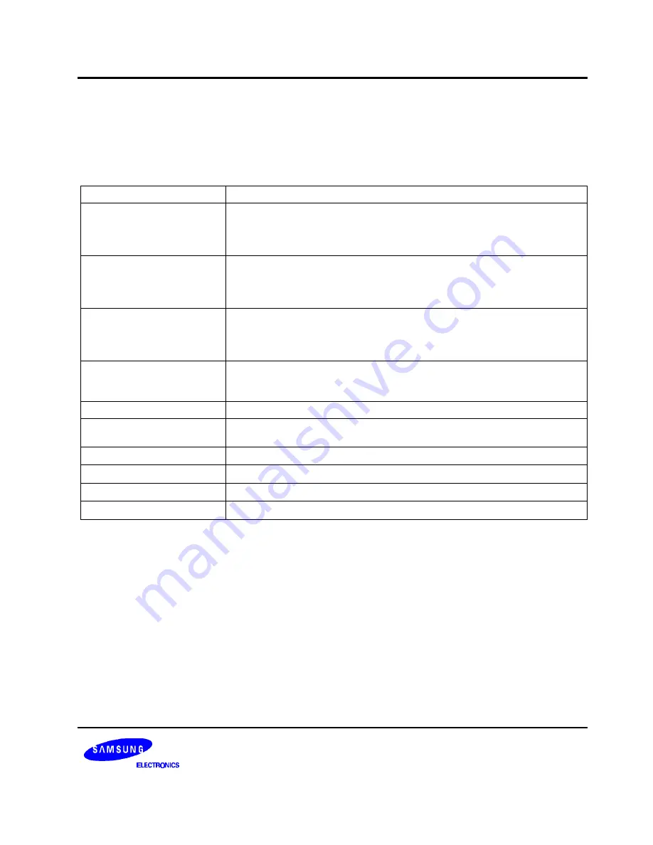
RECOMMENDED CONNECTIONS FOR UNUSED PINS
To reduce overall power consumption, please configure unused pins according to the guidelines described in
Table 8-2.
Table 8-2. Unused Pin Connections for Reducing Power Consumption
Pin/Share Pin Names
Recommended Connection
P0.0/INT4
P0.1/
SCK
P0.2/SO
P0.3/SI
Input mode: Connect to V
DD
Output mode: No connection
P1.0/INT0
P1.1/INT1
P1.2/INT2
P1.3/TCL0
Connect to V
DD
(1)
P2.0/TCLO0
P2.1
P2.2/CLO
P2.3/BUZ
Input mode: Connect to V
DD
Output mode: No connection
P3.2–P3.3
P3.1/LCDSY
P3.0/LCDCK
Input mode: Connect to V
DD
Output mode: No connection
P8.0/SEG24–P8.7/SEG31
No connection
(2)
SEG0–SEG23
COM0–COM3
No connection
V
LC0
–V
LC2
No connection
XT
IN
Connect XT
IN
to V
SS
(Set SCMOD.2 to “1”)
XT
OUT
No connection
TEST
Connect to V
SS
NOTES:
1.
Digital mode at P1.0 and P1.1
2.
Used as segment
Summary of Contents for C2316
Page 30: ...ADDRESS SPACES KS57C2308 P2308 C2316 P2316 2 22 NOTES ...
Page 168: ...SAM47 INSTRUCTION SET KS57C2308 P2308 C2316 P2316 5 94 NOTES ...
Page 170: ......
Page 206: ...POWER DOWN KS57C2308 P2308 C2316 P2316 8 8 NOTES ...
Page 210: ...RESET KS57C2308 P2308 C2316 P2316 9 4 NOTES ...
Page 222: ...I O PORTS KS57C2308 P2308 C2316 P2316 10 12 NOTES ...
Page 272: ...LCD CONTROLLER DRIVER KS57C2308 P2308 C2316 P2316 12 24 NOTES ...
Page 280: ...SERIAL I O INTERFACE KS57C2308 P2308 C2316 P2316 13 8 NOTES ...
Page 294: ...MECHANICAL DATA KS57C2308 P2308 C2316 P2316 15 2 NOTES ...
Page 310: ...KS57P2308 P2316 OTP KS57C2308 P2308 C2316 P2316 16 16 NOTES ...
Page 318: ......
Page 320: ......
Page 322: ......
Page 325: ......
Page 327: ......


