KS57C2308/P2308/C2316/P2316
LCD CONTROLLER/DRIVER
12-3
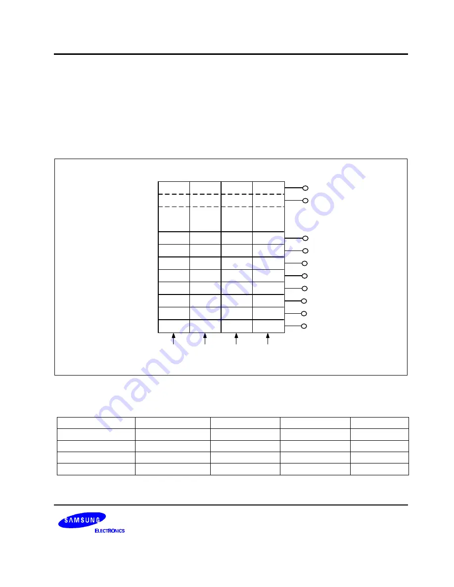
LCD RAM ADDRESS AREA
RAM addresses of bank 1 are used as LCD data memory. These locations can be addressed by 1-bit, 4-bit
instructions. When the bit value of a display segment is "1", the LCD display is turned on; when the bit value is
"0", the display is turned off.
Display RAM data are sent out through segment pins SEG0–SEG31 using a direct memory access (DMA)
method that is synchronized with the f
LCD
signal. RAM addresses in this location that are not used for LCD
display can be allocated to general-purpose use.
SEG0
1E0H
1E1H
1FAH
1FBH
1FCH
1FDH
1FEH
1FFH
1F9H
1F8H
COM3
COM2
COM1
COM0
BIT0
...
...
P8.0
P8.1
P8.2
P8.3
P8.4
P8.5
P8.6
P8.7
BIT1
...
...
BIT2
...
...
BIT3
...
...
SEG1
SEG24
SEG25
SEG26
SEG27
SEG28
SEG29
SEG30
SEG31
Figure 12-3. LCD Display Data RAM Organization
Table 12-1. Common Signal Pins Used per Duty Cycle
Display Mode
COM0 Pin
COM1 Pin
COM2 Pin
COM3 Pin
Static
Selected
N/C
N/C
N/C
1/2
Selected
Selected
N/C
N/C
1/3
Selected
Selected
Selected
N/C
1/4
Selected
Selected
Selected
Selected
NOTE
: N/C = no connection is required.
Summary of Contents for C2316
Page 30: ...ADDRESS SPACES KS57C2308 P2308 C2316 P2316 2 22 NOTES ...
Page 168: ...SAM47 INSTRUCTION SET KS57C2308 P2308 C2316 P2316 5 94 NOTES ...
Page 170: ......
Page 206: ...POWER DOWN KS57C2308 P2308 C2316 P2316 8 8 NOTES ...
Page 210: ...RESET KS57C2308 P2308 C2316 P2316 9 4 NOTES ...
Page 222: ...I O PORTS KS57C2308 P2308 C2316 P2316 10 12 NOTES ...
Page 272: ...LCD CONTROLLER DRIVER KS57C2308 P2308 C2316 P2316 12 24 NOTES ...
Page 280: ...SERIAL I O INTERFACE KS57C2308 P2308 C2316 P2316 13 8 NOTES ...
Page 294: ...MECHANICAL DATA KS57C2308 P2308 C2316 P2316 15 2 NOTES ...
Page 310: ...KS57P2308 P2316 OTP KS57C2308 P2308 C2316 P2316 16 16 NOTES ...
Page 318: ......
Page 320: ......
Page 322: ......
Page 325: ......
Page 327: ......


