


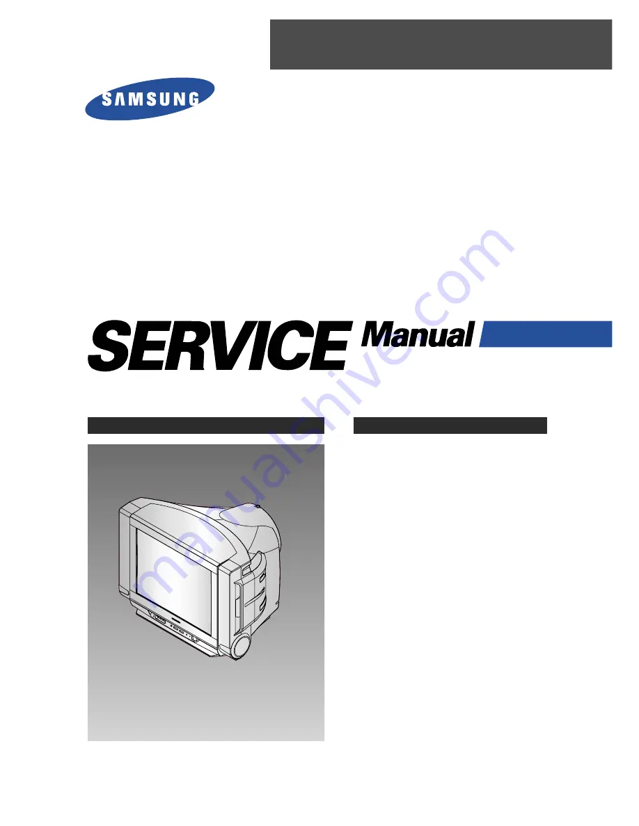
COLOR TELEVISION RECEIVER
Chassis :
KS2A(P) (Rev. 2)
Model :
CS21S8NAS/MUR
COLOR TELEVISION RECEIVER
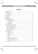
CONTENTS
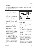
Precautions
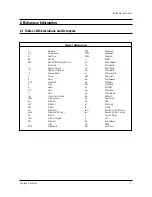
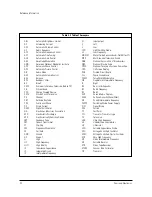
Reference Information
Specifications
Alignment and Adjustments
Troubleshooting
Exploded Views and Parts List
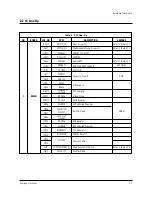
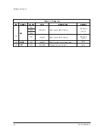
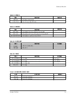
Electrical Parts List
Block Diagrams
Wiring Diagram
Schematic Diagrams
1.
2.
3.
4.
5.
6.
7.
8.
9.
10.
Summary of Contents for CS21S8MUR
Page 11: ...2 6 Samsung Electronics MEMO ...
Page 13: ...3 2 Samsung Electronics MEMO ...
Page 53: ...8 Block Diagrams Samsung Electronics Schematic Diagrams 8 1 8 1 Power Diagram ...
Page 54: ...8 2 Block Diagram Schematic Diagrams 8 2 Samsung Electronics ...
Page 62: ...Samsung Electronics Schematic Diagrams 10 7 10 7 PIP ...
Page 63: ...Schematic Diagrams 10 8 Samsung Electronics 10 8 VIDEO SWITCH ...
Page 64: ...9 2 Samsung Electronics MEMO ...