Circuit Description
13-6
Samsung Electronics
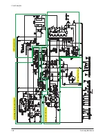
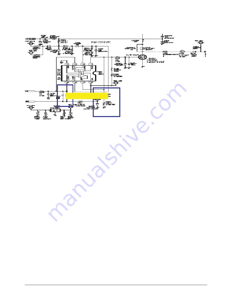
13-2-3 E/W Circuit Block
E
t
i
u
c
r
i
C
n
o
i
t
c
e
r
r
o
C
T
H
E
ⓐ
Understanding of E/W Circuit
▶
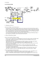
What is an E/W (East / West) Correction Circuit?
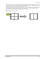
- If the bias angle of a picture widens, the distance from the center of a picture to each corner becomes farther as it moves to
periphery. This causes the picture being distorted (Picture Lowering) horizontally in a shape of a spool because of the strong
bias at four corners where are the farthest from the center. E/W is a circuit which corrects the spool-shape on the left and right
part by crossing Parabollic wave form over the horizontal output board and controls the current which flows through terminal
no.47. Parabollic wave comes out from terminal no.47 of CXA2165 CHROMA IC(IC31)
It also controls the horizontal-related factors of Factory data such as picture size, size change and Parabola gain change. It
has an essential role of minimizing the picture swaying (High Voltage Regulation)
ⓑ
E/W Circuit Constitution and Operation
▶
E/W Circuit Constitution and Operation Principles.
- E/W circuit consists of KA393(comparator), FQP630(output TR), and other parts. This uses a method in which PWM controls
the circuit using a comparator. The advantage of this PWM Control method is that POWER Loss hardly occurs and
generates little heat when using low H/S.
Input E/W signal to terminal no 3,5 of IC401(KA393) and carrier wave to terminal no 2,6. Carrier wave can be made by
reducing the horizontal collector voltage and integrating the wave form using D405,R414 and C406.
Then the carrier wave is compared with E/W signal in IC401 and outputs PWM(Pulse Width Modulation) wave form. Bias
current shall be controlled using Q404.
Picture swaying occurs as the picture brightness varies. To correct this, control the high voltage regulation using
Q401(1N7000), R433 and C411 That is, Q401 is a circuit for correcting Static Regulation and used to prevent the picture
size changing as the picture brightness varies.
It detects the ABL voltage and inputs to Q401 Gate through R423 resistance. Then the ABL voltage change is sent to
IC401(KA393) output and controls the DC of Q404(FQP630) Gate terminal, to keep the picture size from changing.
▶
E/W Circuit Constitution and Operation Principle.
Also, E/W circuit functions as a compensatory circuit against the picture shaking by reversely compensating the picture
swaying. This is possible by inputting ABL voltage to E/W using R433 as the picture brightness varies.
There are H,V, PIN-COMP as well in Factory data and these correct the high voltage regulation. If the H-COMP capacity
Summary of Contents for CS29Z30SPBXBWT
Page 10: ...1 6 Samsung Electronics MEMO...
Page 18: ...Alignment Adjustment 3 4 Samsung Electronics...
Page 67: ...MEMO Samsung Electronics 5 24...
Page 87: ...7 6 Samsung Electronics MEMO...
Page 119: ...12 6 Samsung Electronics MEMO...

