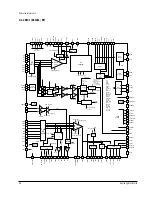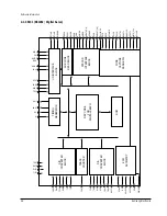
Reference Information
Samsung Electronics
2-11
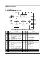
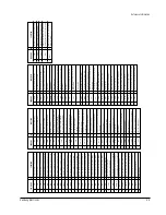
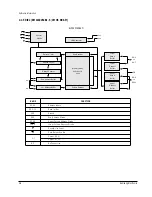
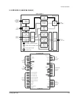
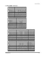
N A M E
M P 7
M P 6
M P 5
M P 4
M P 3
M P 2
M P 1
M P 0
V
D D 2
V
S S 2
R T C I
VDD
1 2 C
S A
V
S S A 1
R ( C r )
C
V
D D A 1
G ( Y )
VBS
V
D D A 2
B ( C b )
CVBS
V
D D A 3
V
S S A 2
V
S S A 3
X T A L
X T A L 1
I / O
I
I
I
I
I
I
I
I
I
I
I
I
I
I
O
O
I
O
O
I
O
O
I
I
I
O
I
PIN
9
1 0
1 1
1 2
1 3
1 4
1 5
1 6
1 7
1 8
1 9
2 0
2 1
2 2
2 3
2 4
2 5
2 6
2 7
2 8
2 9
3 0
3 1
3 2
3 3
3 4
3 5
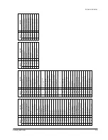
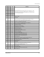
FUNCTION
Digital supply voltage 2
Digital ground 2
Real Time Control input. If the LLC1 clock is provided by an SAA7111 or SAA7151B, RTCI should be
connected to the RTCO pin of the respective decoder to improve the signal quality.
Sense input for 12C bus voltage;connect to 12C bus supply
Select 12C address; low selects slave address 88h, high selects slave address 8Ch.
Analog ground 1 for Red (Cr), C(CVBS), Green(Y) outputs
Analog ground 3 for the DAC reference ladder and the oscillator
Crystal oscillator output
Crystal oscillator input; if the oscillator is not used, this pin should be connected to ground.
Analog output of Red (Cr)signal
Analog output of Chrominance (CVBS) signal
Analog supply voltage 1 for R(Cr), C(CVBS) outputs
Analog output of Green(Y) signal
Analog output of VBS (CVBS) signal
Analog supply voltage 2 for VBS(CVBS), Green(Y) outputs
Analog output of Blue(Cb) signal
Analog output of CVBS(CSYNC) signal
Analog supply voltage 3 for Blue(Cb)and CVBS(CSYNC), outputs
Analog ground 2 for VBS (CVBS), Blue(Cb), CVBS(CSYNC)outputs
Double speed 54 MHzMPEG port. It is an input for "CCIR 656" style multiplexed Cb, Y, Cr data.
Data are sampled on the rising and falling clock edge;data sampled on the risting edge then are sent to
the encoding part of the device, data sampled on the falling edge are sent to the RGB part of the device.
(or vice verse, depending on programming)
V
D D A 4
XCLK
V
S S 3
V
D D 3
RESN
S C L
S D A
TTXRQ
T T X
I
O
I
I
I
I
I / O
O
I
3 6
3 7
3 8
3 9
4 0
4 1
4 2
4 3
4 4
Analog supply voltage 4 for the DAC reference ladder and the oscillator
Clock output of the crystal oscillator
Digital supply ground 3
Digital supply 3
12C serial clock input
12C serial data input/output
Teletext Request output, indicating when text bits are requested
Teletext bit stream input
Reset input, active LOW. After reset is applied, all digital I/Os are in input mode; PAL-
Blackburst on CVBS, VBS and C;RGB outputs set to lowest voltage.
The 12C-bus receiver waits for the START condition.
Summary of Contents for DVD-C600
Page 23: ...Reference Information 2 16 Samsung Electronics MEMO ...
Page 49: ...4 24 Samsung Electronics Disassembly and Reaasembly MEMO ...
Page 79: ...Troubleshooting 6 10 Samsung Electronics MEMO ...
Page 85: ...Exploded Views and Parts List 7 6 Samsung Electronics MEMO ...
Page 91: ...8 6 Samsung Electronics Electrical Parts List MEMO ...
Page 95: ...PCB Diagrams 10 2 Samsung Electronics 10 1 Main COMPONENT SIDE SOLDER SIDE ...
Page 96: ...PCB Diagrams Samsung Electronics 10 3 10 2 Jack ...
Page 97: ...PCB Diagrams 10 4 Samsung Electronics 10 3 S M P S ...
Page 98: ...PCB Diagrams Samsung Electronics 10 5 10 4 Front COMPONENT SIDE SOLDER SIDE ...
Page 99: ...PCB Diagrams 10 6 Samsung Electronics 10 5 Key COMPONENT SIDE SOLDER SIDE ...
Page 100: ...PCB Diagrams Samsung Electronics 10 7 10 6 Head Phone 10 7 Deck COMPONENT SIDE SOLDER SIDE ...
Page 101: ...PCB Diagrams 10 8 Samsung Electronics 10 8 Sensor 10 9 Motor ...
Page 103: ...Wiring Diagram 11 2 Samsung Electronics MEMO ...
Page 105: ...Schematic Diagrams 12 2 Samsung Electronics 12 1 S M P S ...
Page 106: ...Schematic Diagrams Samsung Electronics 12 3 12 2 Main Power Supply ...
Page 107: ...Schematic Diagrams 12 4 Samsung Electronics 12 3 Main Micom ...
Page 108: ...Schematic Diagrams Samsung Electronics 12 5 12 4 Servo ...
Page 109: ...Schematic Diagrams 12 6 Samsung Electronics 12 5 Video Encoder ...
Page 110: ...Schematic Diagrams Samsung Electronics 12 7 12 6 Video CVBS Output Y Output C Output ...
Page 111: ...Schematic Diagrams 12 8 Samsung Electronics 12 7 Audio DAC ...
Page 112: ...Schematic Diagrams Samsung Electronics 12 9 12 8 Audio ...
Page 113: ...Schematic Diagrams 12 10 Samsung Electronics 12 9 RF ...
Page 114: ...Schematic Diagrams Samsung Electronics 12 11 12 10 ZiVA ...
Page 115: ...Schematic Diagrams 12 12 Samsung Electronics 12 11 DSP ...
Page 116: ...Schematic Diagrams Samsung Electronics 12 13 12 12 Front Micom VFD Display ...
Page 118: ...Schematic Diagrams Samsung Electronics 12 15 12 14 Head Phone ...
Page 119: ...Schematic Diagrams 12 16 Samsung Electronics 12 15 Key ...
Page 120: ...Schematic Diagrams Samsung Electronics 12 17 12 16 Deck ...
Page 121: ...Schematic Diagrams 12 18 Samsung Electronics 12 17 Deck Control ...
Page 122: ...Schematic Diagrams Samsung Electronics 12 19 12 18 Remote Control ...
Page 123: ...Schematic Diagrams 12 20 Samsung Electronics MEMO ...


