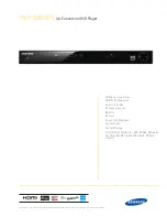
background image

DVD PLAYER

DVD-C700

SERVICE 

1. Precautions

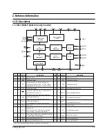
2. Reference Information

3. Product Specification

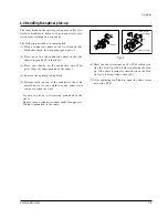
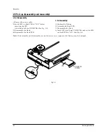
4. Disassembly and Reassembly

5. Circuit Descriptions

6. Troubleshooting

7. Exploded Views and Parts List

8. Electrical Parts List
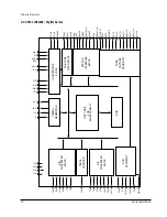
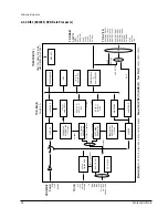
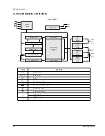
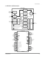
9. Block Diagrams

10. PCB Diagrams

11. Wiring Diagram

12. Schematic Diagrams

Manual 

DVD PLAYER

CONTENTS

SERVICE MANUAL

DVD-C700

DIGITAL VIDEO

DVD / VIDEO-CD / CD PLAYER  DVD-C700

DOLBY DIGITAL DECODER BUILT-IN

5

SPATIALIZER

N-2-2

ELECTRONICS

© Samsung Electronics Co., Ltd. 

JAN. 2000

Printed in Korea

AH68-00314A

Summary of Contents for DVD-C700

Page 1: ...ing 7 Exploded Views and Parts List 8 Electrical Parts List 9 Block Diagrams 10 PCB Diagrams 11 Wiring Diagram 12 Schematic Diagrams Manual DVD PLAYER CONTENTS SERVICE MANUAL DVD C700 DIGITAL VIDEO DVD VIDEO CD CD PLAYER DVD C700 DOLBY DIGITAL DECODER BUILT IN 5 SPATIALIZER N 2 2 ELECTRONICS Samsung Electronics Co Ltd JAN 2000 Printed in Korea AH68 00314A ...

Page 2: ...rwriters Laboratories UL 1270 40 7 With the instrument s AC switch first in the ON position and then in the OFF position measure from a known earth ground metal water pipe conduit etc to all exposed metal parts of the instrument antennas handle brackets metal cabinets screw heads metallic overlays control shafts etc espe cially any exposed metal parts that offer an electri cal return path to the c...

Page 3: ...ched out of place or frayed wiring Do not change spacing between a component and the printed circuit board Check the AC power cord for damage 5 Components parts and or wiring that appear to have overheated or that are otherwise damaged should be replaced with components parts and or wiring that meet original specifications Additionally determine the cause of overheating and or damage and if necess...

Page 4: ...nd lead last 2 The service precautions are indicated or printed on the cabinet chassis or components When servic ing follow the printed or indicated service precau tions and service materials 3 The components used in the unit have a specified flame resistance and dielectric strength When replacing components use components which have the same ratings Components i enti fied by shading by or by in t...

Page 5: ...posure of the assem bly 3 Use only a grounded tip soldering iron to solder or unsolder ESD devices 4 Use only an anti static solder removal devices Some solder removal devices not classified as anti static can generate electrical charges suffi cient to damage ESD devices 5 Do not use freon propelled chemicals These can generate electrical charges sufficient to damage ESD devices 6 Do not remove a ...

Page 6: ... sheet This gives them the same ground as the sheet 4 Remove the optical pick up block 5 Perform work on top of the conductive sheet Be careful not to let your clothes or any other static sources to touch the unit Be sure to put on a wrist strap grounded to the sheet Be sure to lay a conductive sheet made of copper etc Which is grounded to the table Fig 1 3 6 Short the short terminal on the PCB wh...

Page 7: ...d into Main PCB MCN06 See Fig 1 4 3 Disassemble the Deck 4 Disassemble the Deck PCB 1 5 2 Assembly 1 Replace the Pick up 2 Assemble the Deck PCB 3 Reassemble the Deck 4 Insert FPC into Main PCB MCN06 and switch SW1 on Deck PCB to ON See Fig 1 4 SW1 ON OFF FPC TO MAIN PCB MCN06 Note If the assembly and disassembly are not done in correct sequence the Pick up may be damaged Fig 1 4 ...

Page 8: ...MUTE 9 I DFS 10 I DEM0 11 Soft mute pin When this pin goes H soft mute cycle is initiated When returning L the output mute releases Audio serial data input pin 64fs clock is recommended to be input on this pin Audio serial data input pin 2 s complement MSB first data is input on this pin Double speed sampling mode pin Internal pull down pin L normal speed H double speed L R clock pin De emphasis f...

Page 9: ...13 E 12 VREFEQ 11 RREF 10 RREFEQ 9 RREFBF 8 DDVD 7 CDVD 6 BDVD 5 ADVD 4 DCD 3 CCD 2 BCD 1 ACD to RF EQ TUNING BLOCK AGC HOLD OOH MUX AGC_DET RF MUX VREF GENERATOR CDRSEL 00H EQ VC AMP D D D D MUX3 GAIN_TE3 02H GCA OFSTHOLD TEOFST 04H TBAL 01H TE38 SUB RF MUX D1 B1 C1 A1 FE GAIN_FE 03H FE_0FST 05H CDRSEL 00H ANALOG VC AMP ALPC LDONB 00H FOFST OFSTHOLD MUX TESEL OOH OFSTHOLD ABCD_OFST O6H ENVELOPE F...

Page 10: ...n port SERVO defect max time setting Peak hold time constant connection port PLL defect min time setting 39 ABCD ENVP ENVB ENV DGND FOKTH FOKB DFCT_CP1 DFCT_CP2 O O I O P 62 61 60 59 58 57 56 55 54 53 52 51 50 49 Output port of peak detector for defect AC coupling input port for defect Power voltage input port for digital circuit Resistance connection port for PLL defect comparat ing level setting...

Page 11: ...L EFMI RFI ASYDVD ASYCD EFM EFMOA PLLHD INTO_224 FDCTL MAGICO EQCTL VCTRL RVCO PLCK EFMRTD RPD RFD PLLLOCK MDOUT 3 0 PSB SENSE MDATA 7 0 MRDB MWRB CSB DAB SCOR SQSI SQCK LDONB TLKB FLKB DIRC PS1 SSTOP PSO SMON LOCK DFCT FOKB MIRR TZCA PHI1 XOUT XO XI TEST RSTB TILTO TILTI ROM DSP CORE FOR DIGITAL SERVO TIMING GENERATOR I O INTERFACE BLOCK SUB CODE READ BLOCK SYSCON INTERFACE BLOCK WIDE CAPTURE RAN...

Page 12: ...r signal input pin PLL hold signal from micom Servo interrupt monitor pin PLL logic block VDD power supply pin PLCK Frequency lock detect output H Lock L Unlock Latched EFM output signal PLL logic block VSS power supply pin Resistor pin for VCO GAIN Gain adjust resister for frequence detector Gain adjust resister for phase detector Control voltage for VCO Input for hysteresis control of FD output ...

Page 13: ...35KHz EFM DEMOD SUBCODE I F CD G V CD CD DA SQ VCD DVDP DEINTERLEAVE RAM CONTROL 6 4 3 trans ID ECC EDC DESCRAMBLER MICOM I F M M TO MICOM 15 MDAT 7 0 MRZA ZCS MWR MRD ZIRQZD ZWAIT ZRST TO DRAM 256K 16 32 DD 15 0 DADR 8 0 ZRAS ZUCAS ZLCAS ZOE 1 0 ZWE 1 0 TO AV 13 SDATA 0 CDATA SDATA 1 LRCK SDATA 2 BCLK SDATA 3 C2PO SDATA 4 SQDT SDATA 5 WFSY SDATA 6 SOS1 SDATA 7 SQCK DATREQ CSTROBE DTER DATACK TOS ...

Page 14: ...DRAM data bus 33 DD6_BI FUNCTION PIN NAME Digital GND 5V 97 DVSS System clock output for 33 8688MHz 96 CK33MO_OUT System clock input for 33 8688MHz 95 CK33MI_IN Digital out 92 TX_OUT Good frame sync detection result output H active 93 GFS_OUT Frame sync out 91 FRSYZ_OUT Digital GND 0V 90 DVSS Digital GND 0V 89 DVSS Digital GND 0V 88 DVSS Digital GND 0V 87 DVSS Digital power 5V 86 DVDD Digital powe...

Page 15: ...Lower Data out Buffer Upper Data in Buffer Upper Data out Buffer Vcc Vss RAS UCAS LCAS W FUNCTION Address Inputs Data in Out Ground Row Address Strobe Upper Column Address Strobe Lower Column Address Strobe Read Write Input Data Output Enable Power 5V Power 3 3V No Connection Refresh Timer Refresh Control AO A8 Refresh Counter Row Address Buffer Col Address Buffer Row Decoder Column Decoder Memory...

Page 16: ...d Content Descrambled Compressed Content Decompressed Content Display Content LOGIC DIAGRAM HADDR 2 0 RD HDATA 7 0 WAIT DTACK INT HOST8SEL Host Interface Signals Video Interface Signals DVD CD Interface Signals Audio Interface Signals SDRAM EDO Interface Signals Global Interface Signals DA DATA 0 3 DA LRCK DA BCK DA XCK DA IEC EDO CAS EDO RAS LDQM MDATA 15 0 MADDR 20 0 MWE ROM CS SD CLK SD CAS 1 0...

Page 17: ... 2 3 VSS VDD SP AP 19 RTC1 CbCr Y CbCr 24 R Cr VSSA G Y B Cb CVBS CSYNC VBS CVBS C CVBS A BLOCK DIAGRAM NAME res SP A P LLC1 V SS1 V DD1 RCV1 RCV2 I O I I I I I I O I O PIN 1 2 3 4 5 6 7 8 FUNCTION Reserved pin do not connect Test Pin connected to digital ground for normal operation Test Pin connected to digital ground for normal operation Line Locked Clock input this is the 27 MHz master clock Di...

Page 18: ... for R Cr C CVBS outputs Analog output of Green Y signal Analog output of VBS CVBS signal Analog supply voltage 2 for VBS CVBS Green Y outputs Analog output of Blue Cb signal Analog output of CVBS CSYNC signal Analog supply voltage 3 for Blue Cb and CVBS CSYNC outputs Analog ground 2 for VBS CVBS Blue Cb CVBS CSYNC outputs Double speed 54 MHzMPEG port It is an input for CCIR 656 style multiplexed ...

Page 19: ...TEST2 1 NMI WDTOUT P00 to P07 AD0 to AC7 P10 to P17 AD8 to AD15 A8 toA15 P20 to P27 A0 to A7 A16 to A23 P30 RD P31 WR P32 HWR P33 WAIT P34 BUSRQ P35 BUSAK P36 R W P37 RAS P40 CS0 CAS0 P41 CS1 CAS1 P42 CX2 CAS2 PORT A High Frequency OSC Low Frequency OSC INTERRUPT CONTROLLER WATCH DOG TIMER PORT 0 PORT 2 PORT 3 CS WAIT CONTROLLER 3 BLOCK PORT 1 10 BIT 8CH A D CONVERTER SERIAL I O CH 0 SERIAL I O CH...

Page 20: ...D RXDO Serial data clock SCLK SCLKO RF control data MD TXD1 RF data latch STB 094 RF control clock MC SCLK1 Address mode H 8 bit mode AM8 AM8 16 Clock output System clock 2 CLK CLK VCC Vcc GND GND Vss High frequency OSC in X1 X1 High frequency OSC out X2 X2 External access CS41 CS40 EA EA Master reset from FRONT MRST RESET FUNCTION ASSIGNED NAME PORT NAME No I O I I O O O O I I I I I I O I O I I O...

Page 21: ... Vcc A17 A14 A13 A8 A9 A11 OE VPP A10 CE DQ7 DQ6 DQ4 DQ4 DQ3 32 31 30 29 28 27 26 25 24 23 22 21 20 19 18 17 TOP VIEW Output Enable Chip Enable and Prog Logic Output Buffers Y Gating 2 097 152 Bit Cell Matrix Y Decoder A0 A19 Address Inputs OE VPP X Decoder Data Outputs DQ0 DQ7 CE Vcc Vss BLOCK DIAGRAM FUNCTION Address Inputs Chip Enable Input Data Input Outputs Output Enable Input Vcc Syply Volta...

Page 22: ...T1 Low frequency OSC out XT2 GND VSS High frequency OSC in CF1 High frequency OSC out CF2 VDD VDD GND AN0 P80 GND AN1 P81 AN2 P82 HARDWARE MODE SELECT MODE0 AN3 P83 HARDWARE MODE SELECT MODE1 AN4 P84 HARDWARE MODE SELECT MODE2 AN5 P85 HARDWARE MODE SELECT MODE3 AN6 P86 HARDWARE MODE SELECT MODE4 AN7 P87 Request to front micom RRQ P70 INT0 Roulette sensor P71 INT1 P72 INT2 REMOCON data in REMOCON P...

Page 23: ...Reference Information 2 16 Samsung Electronics MEMO ...

Page 24: ...hes Reading Speed 3 9 to 4 6 ft sec Compact Disc Maximum Play Time 20min VCD 5 inches Reading Speed 3 9 to 4 6 ft sec Maximum Play Time 74min Video Audio Composite Video 2 Channel 1 0Vp p 75ohm load Y 1 0Vp p 75ohm load Video Output Component Video Pr 0 70Vp p 75ohm load Pb 0 70Vp p 75ohm load S Video Luminance Signal 1 0Vp p 75ohm load Color Signal 0 286Vp p 75ohm load 2 channel L 1 L R 2 R 5 1 c...

Page 25: ...ed 1 2 to 1 4m sec Maximum Play Time 74min Video Audio R Red 0 714Vp p 75ohm load G Green 0 714Vp p 75ohm load Scart Jack B Blue 0 714Vp p 75ohm load Video Output Composite Video 1 0Vp p 75ohm load Luminance Signal 1 0Vp p 75ohm load Color Signal 0 286Vp p 75ohm load Component Video 2 Channel 1 0Vp p 75ohm load S Video Luminance Signal 1Vp p 75ohm load Color Signal 0 286Vp p 75ohm load Scart Jack ...

Page 26: ... up the Door Tray in the direction of arrow A by both hand to remove 3 Close Tray Œ and power off Note If Tray Œ doesn t open insert a Screw driver into the Emergency hole ˇ as shown in detailed draw ing and then turn it in the direction of arrow B Open Tray manually CLOSE OPEN Œ TRAY DOOR TRAY A A ˇ EMERGENCY HOLE Bottom View SCREW DRIVER B Fig 4 1 Door Tray Removal ...

Page 27: ...and Reaasembly 4 1 2 Top Cabinet Removal 1 Remove 5 Screws Œ on the back Top Cabinet 2 Remove 4 Screws ˇ on the left and right side 3 Lift up the Top Cabinet in direction of arrow Œ 5 SCREWS 2 SCREWS ˇ 2 SCREWS Fig 4 2 Top Cabinet Removal ...

Page 28: ...Ø FRONT PCB Fig 4 3 Ass y Front Panel Front PCB Headphone PCB Removal 4 1 3 Ass y Front Panel Front PCB Headphone PCB Removal 1 Remove 2 Screws Œ and disassemble the Ass y Front Panel 2 Remove Knob Shuttle ˇ 3 Remove 11 Screws ˆ and disassemble the Front PCB Ø 4 Remove 2 Screws and disassemble the Headphone PCB ...

Page 29: ...Removal 1 Remove 2 Screws 4 Screws Region Europe Œ 2 Remove 3 Screws and lift the Jack PCB ˇ up CAUTIONS 1 When disassembling switch the SW1 to OFF on the Deck PCB and remove the FPC connected to MCN06 on Main PCB See Fig 1 4 on page 1 6 2 When assembling insert the FPC into the MCN06 on Main PCB and switch SW1 to ON on the Deck PCB See Fig 1 4 on page 1 6 3 Disconnect FPC Pin 36 from MCN06 on Mai...

Page 30: ...Disassembly and Reaasembly Samsung Electronics 4 5 MAIN PCB JACK PCB S M P S PCB TO HEADPHONE PCB CON23 CORE FERRITE Fig 4 5 Wire Arrangement Top View Wire Arrangement ...

Page 31: ...ronics Disassembly and Reaasembly Œ 2 SCREWS 2 SCREWS ˇ BRACKET PCB 4 SCREWS 4 1 5 Ass y Deck Removal 1 Remove 4 Screws Œ and Bracket PCB ˇ 2 Remove 4 Screws from the Ass y Deck and lift it up Fig 4 6 Ass y Deck Removal ...

Page 32: ...Disassembly and Reaasembly Samsung Electronics 4 7 JACK PCB MAIN PCB S M P S PCB HEADPHONE PCB KEY PCB FRONT PCB 4 2 PCB Location Fig 4 7 PCB Location ...

Page 33: ...MAIN PCB MCN02 Ø CN5 DECK PCB MAIN PCB MCN06 PCN03 S M P S PCB MAIN PCB MCN01 Ô JCN04 JACK PCB HEADPHONE PCB CON23 Ò FCN01 FRONT PCB JACK PCB JCN02 Ú Æ FCN04 FRONT PCB MAIN PCB MCN04 ı TCN03 DECK PCB MAIN PCB MCN05 CT1 CT2 CT3 CT4 CT5 CT6 CT7 CT8 CT9 CT1 S M P S PCB JACK PCB FRONT PCB Œ Ô ˇ ˆ Ú Ø ı Ò Æ MAIN PCB CT6 CT7 CT9 CT5 CT2 CT3 CT4 CT8 4 3 Connector Diagram Fig 4 8 Connector Diagram ...

Page 34: ...ee Fig 1 4 on page 1 6 1 Insert a Screw driver into Emergency hole Œ and turn Gear Load ˇ in the direction of arrow A 2 When the Tray comes out a little pull it in the direction of arrow B by hand 3 Disconnect Flat Cable Ø 4 Pull the Tray to disassemble while simultaneously pushing the Stopper ˆ in direction of arrow C CAUTION Do not stain with grease Pick Up Lens Turn table Roulette Disc Tray Dis...

Page 35: ... Electronics Disassembly and Reaasembly 4 4 2 Tray Roulette Removal 1 Remove Screw Π2 Lift up the Tray Roulette Fig 4 10 Tray Roulette Removal ΠSCREW TRAY ROULETTE TRAY DISC Assembly Point TRAY ROULETTE TRAY DISC ...

Page 36: ... 2 Screws and lift up the Bracket Worm Ass y ˆ 4 Remove Belt Ø 5 Remove Washer and the Gear Roulette 6 Remove 2 Screws and the Shaft Worm Ass y 7 Remove 2 Screws Ô and the Worm Motor Fig 4 11 Bracket Worm Ass y Removal Bottom View SENSOR PCB SENSOR PCB 2 SCREWS 2 SCREWS Ø BELT Œ LCN02 ˆ BRACKET WORM ASS Y WASHER GEAR ROULETTE SHAFT WORM ASS Y Ô 2 SCREWS WORM MOTOR ˇ HOOK ˇ HOOK ˇ HOOK ˇ HOOK ˇ HOO...

Page 37: ...t DATIL A 3 Remove the Ass y P U Deck Ø in direction of arrow C while simultaneously pushing the 2 Hooks ˆ in direction of arrow B CAUTION Do not stain with grease Pick Up Lens Turn table Roulette Disc Tray Disc Belt Fig 4 12 Ass y P U Deck Removal Œ RUBBER PAD PROTECT CAUTION Suface of adhesion ˆ HOOK ˆ HOOK B B Ø ASS Y P U DECK C SLIDER RACK Assemlby Point SLIDER RACK A CLOSE OPEN EMERGENCY HOLE...

Page 38: ...3 4 4 5 Slider Rack Removal 1 Remove the Slider Rack in direction of arrow B while simultaneously pushing the Lever Locker Πin direction of arrow A Fig 4 13 Slider Rack Removal 1 ΠLEVER LOCKER A B SLIDER RACK SLIDER RACK ΠLEVER LOCKER Assembly Point ...

Page 39: ...al 1 Remove Belt Pulley Œ 2 Push the Hook ˇ in the Boss in the direction of arrow 3 Lift up the Gear Pulley CAUTION Do not stain with grease Pick Up Lens Turn table Roulette Disc Tray Disc Belt Fig 4 14 Belt Pulley Gear Pulley Removal Œ BELT PULLEY GEAR PULLEY BOSS GEAR PULLEY BOSS ˇ HOOK ...

Page 40: ...ction of arrow and lift up Gear Tray Œ 2 Push the Hook below the Gear Convert ˇ in the direction of arrow and lift up Gear Convert ˇ 3 Push the Hook below the Gear Cam in the direction of arrow and lift up Gear Cam 4 Remove Gear Load ˆ Fig 4 15 Gear Tray Gear Convert Gear Cam Gear Load Removal Œ GEAR TRAY HOOK ˇ GEAR CONVERT GEAR CAM ˆ GEAR LOAD Bottom Side ...

Page 41: ...er Removal 1 Remove Spring Locker Œ 2 Lift up the Lever Locker pushing the direction of arrow A 3 Remove the Gear Syncro in direction of arrow B while simultaneously pushing the 2 Hooks ˇ Fig 4 16 Spring Locker Lever Locker Removal Œ SPRING LOCKER LEVER LOCKER GEAR SYNCRO ˇ HOOKS A B ...

Page 42: ...ook Œ in the direction of arrow A 4 Hooks in the direction of arrow B and lift up PCB Motor Ass y ˇ 2 Push the 3 Hooks ˆ Ø in the direction of arrow C and lift up PCB Switch Ass y Fig 4 17 PCB Motor Ass y PCB Switch Removal Œ HOOK A 2 HOOKS 2 HOOKS B B ˇ PCB MOTOR ASS Y PCB SWITCH HOOK ˆ HOOK Ø HOOK C C C ...

Page 43: ... Clamper Removal 1 Pull the Clamper by hand in the direction of arrow B while simultaneously pushing the 4 Hooks Œ in direction of arrow A 2 Remove the Magnet ˇ 3 Lift up the Plate Chuck Fig 4 18 Clamper Removal CLAMPER PLATE CHUCK ˇ MAGNET Œ 4 HOOKS B A A A A ...

Page 44: ...Push the Stopper in the direction of arrow A 4 Pull the Shaft P U ˆ in the direction of arrow B to remove 5 Lift up the Pick up Ø in the direction of arrow C CAUTION Do not stain with grease Pick Up Lens Turn table Roulette Disc Tray Disc Belt Fig 4 19 Pick Up Ass y Removal Œ WASHER GEAR FEED U CN2 ˇ FPC STOPPER A B ˆ SHAFT P U ˆ SHAFT P U Ø PICK UP ASS Y C ...

Page 45: ...2 PCB Deck Removal 1 Remove the soldering of CN4 Œ Pin 6 2 Remove the Soldering pole of Motor Feed pole 3 Remove 3 Screws ˇ 4 Remove the FPC from Motor Spindle Ass y side 5 Remove PCB Deck ˆ Fig 4 20 PCB Deck Removal Œ CN4 FEED MOTOR ˇ 3 SCREWS ˆ PCB DECK FPC ...

Page 46: ...Disassembly and Reaasembly Samsung Electronics 4 21 4 4 13 Spindle Motor Removal 1 Remove 3 Screws Π2 Lift up the Spindle Motor Fig 4 21 Spindle Motor Removal Π3 SCREWS SPINDLE MOTOR ...

Page 47: ...sung Electronics Disassembly and Reaasembly 4 4 14 Bracket Deck Ass y Removal 1 Remove 4 Screws Œ 2 Lift up the Bracket Deck Ass y Fig 4 22 Bracket Deck Ass y Removal Œ 4 SCREWS BRACKET DECK ASS Y ˇ SUB CHASSIS ...

Page 48: ...Reaasembly Samsung Electronics 4 23 4 4 15 Assembly of Gear Fig 4 23 Assembly of Gear Œ GEAR CAM GEAR TRAY ˇ GEAR CONVERT TRAY DISC Œ GEAR CAM GEAR TRAY ˇ GEAR CONVERT TIMING POINT 2 TIMING POINT 1 GEAR TRAY Œ GEAR CAM ...

Page 49: ...4 24 Samsung Electronics Disassembly and Reaasembly MEMO ...

Page 50: ...r Vreg Vout Vs Ns Vp Np REGULATOR Common power Ex 120 220V 50 60Hz Fig 5 1 Linear Power Supply Waveform Description Vs t 0 Fig 5 2 Vs t 0 Fig 5 3 Vout t 0 Fig 5 4 Input Common power to transformer Vp The output Vs of transformer is determined by the ratio of 1st Np and 2nd Ns Vs Ns Np x Vp Vout is output DC by diode and condensor ...

Page 51: ...sed by margin design Greater core size and condensor capacity are ne eded because the transformer works on a single power frequency 5 1 1 b S M P S Pulse width modulation method v Vreg Vout 0 t Change by common power Regulator loss Fig 5 5 Terms 1 1st Common power input to 1st winding 2 2nd Circuit followings output winding of transformer 3 f Frequency Switching frequency T Switching cycle 4 Duty ...

Page 52: ...ed power by leakage inductance Fig 5 7 1 Prevent residual high voltage at the terminals of switch during switch off Suppress noise High inverted power occurs at switch PIC1 off because of the 1st winding of transformer V LI xdi dt LI Leakage Induction A very high residual voltage exists on both terminals of PIC1 because dt is a very short 2 SNUBBER circuit protects PIC1 from damage through leakage...

Page 53: ...3 of A K current down PIC2 Diode current down PIC2 C E current down PIC2 C E voltage up PIC1 F B voltage up Out Duty up Transformer 1st current up Transformer 1st power up Vout up Maintain Vout 5 8V 3 If load of 5 8 V terminal decreases or AC input voltage rises and Vout rises above 5 8V then Reverse sequence of the above description Duty down Vout down Maintain 5 8V i e the feedback to maintains ...

Page 54: ...uit 5V Rectified Smoothing Circuit 8V Rectified Smoothing Circuit 8V Rectified Smoothing Circuit 3 3V Rectified VoltageCircuit 5V Rectified VoltageCircuit x2 Motor 8V 1 Port 8V Rectified VoltageCircuit 8V Rectified VoltageCircuit O U T P U T Fig 5 9 5 1 3 b PIC1 STR G6153T Internal Block Diagram Voltage Ref UVLO Vcc Drain Source GND Sense S Q R S Q R OSC Vck 32V Feedback LEB Reset 7 5V 5v Reset Th...

Page 55: ...shows the flow of signal generated by the pick up A B C D signals detected from pick up are converted in to RF signal A B C D via RF summing AMP Fig 5 12 shows the waveform equalizing block diagram for the RF signal It outputs to EQout Pin 86 terminal by initially changing switching AMP gain of DVD and CD and then adjust ing the level in RF SUM AGC It controls RF SUM AGC gain by means of Pin 89 95...

Page 56: ... of DVD EQ and CD EQ are as follows 1 DVD CD EQ control parameter ΠEQG Pin 97 Changes the gain of peak frequency with EQ frequency characteristic Convert PWM signal output from KS1453 into DC via low pass filter EQF Pin 98 Changes the peak frequency with EQ frequency characteristic Convert PWM signal output from KS1453 into DVD via low pass filter ...

Page 57: ... mounted in main board analizes the key commands of front panel or instructions of remote control through communication with Micom FIC1 LC86P6232 of front and controls the devices on board to exe cute the corresponding commands after initializing the devices connected with micom on board at power on 5 3 2 Block Diagram RIC1 RF AMP KS1461 SIC1 DIGITAL SERVO KS1452 VIC1 A V DECODER ZIVA 3 VIC50 VIDE...

Page 58: ...ously CH1 CS2 MIC8 22 EPROM CHIP SELECT CH2 DSPCS DIC1 2 DATA PROCESSOR CHIP SELECT CH3 DVDCS VIC1 206 A V DECODER CHIP SELECT CH4 SRVCS SIC1 10 DIGITAL SERVO CHIP SELECT CH5 WR MIC1 73 MICOM OUTPUT WRITE SIGNAL CH6 RD MIC1 72 MICOM OUTPUT READ SIGNAL CS2 DSPCS DVDCS SRVCS RD WR Fig 5 14 CH1 CS2 MIC8 22 EPROM CHIP SELECT CH2 DSPCS DIC1 2 DATA PROCESSOR CHIP SELECT CH3 DVDCS VIC1 206 A V DECODER CH...

Page 59: ...PROM CHIP SELECT CH2 DSPCS DIC1 2 DATA PROCESSOR CHIP SELECT CH3 DVDCS VIC1 206 A V DECODER CHIP SELECT CH4 SRVCS SIC1 10 DIGITAL SERVO CHIP SELECT CH5 WR MIC1 73 MICOM OUTPUT WRITE SIGNAL CH6 RD MIC1 72 MICOM OUTPUT READ SIGNAL CS2 DSPCS DVDCS SRVCS RD WR Fig 5 16 ...

Page 60: ...ked SERVO When the tracking actuator inclines outwardly as the object lens follows the track during play the SLED motor moves slightly and counteracts the incline 4 CLV SERVO DISC Motor Control SERVO Controls the disc motor to maintain a constant linear velocity necessary for RF signal 5 4 2 Block Diagram Fig 5 17 DISC SLED M T HALL PCB LD PD SPINDLE M T CN1 HA1 HA1 HA2 HA2 SLED SLED AO DO CO BO F...

Page 61: ...in65 of SIC1 FEI Pin39 of RIC1 ABCD 2 PLAY When focus loop closes the loop during focus servo on both pin 65 and pin 75 of SIC1 are controlled by VREF voltage approx 2 5V and pin 1 2 of DRIC2 are approximately 4 5V 2 TRACKING SERVO 1 NORMAL PLAY MODE ΠFor DVD Composite The signal output from PD A B C D of Pick up the tracking error signal pin36 of RIC1 uses the phase difference of A C and B D in ...

Page 62: ...lay mode Move SLED motor slightly by means of PWM signal in SIC1 pin 73 as the tracking actuator moves along with track during play Control to move the entire Pick up as the tracking actuator moves Coarse serach mode In case of long distance search such as chapter serach SIC1 uses sled FG SIC8 pin 1 7 which is generated by rotation of sled motor via hall PCB Then read ID and compute the existing t...

Page 63: ... filled this status is report ed by interrupt to main micom which controls the servo to kick back the pick up to the previous track after mem orizing the last data read from disc until now It takes some times to jump to the previous track and return to the original jump location again The memory will have an empty space because A V decoder reads out data of mem ory When the memory has an empty spa...

Page 64: ...5 3 Waveform Description It measures the timing that data processed in DIC1 at DVD playback STROBE REQ DACK SDATA all 2 2 0 1 0 Fig 6 20 CH1 STROBE DIC1 69 CLOCK CH2 REQ DIC1 70 DATA REQUEST CH3 DACK DIC1 58 DATA ACKNOWLEDGE CH4 SDATA DIC1 60 67 DATA ...

Page 65: ...nd D A conversion of 8bit video data inputted from VIC1 A V decoder by control of MIC1 Micom Video signal converted into analog signal is outputted via amplifier of analog part Main Board Output Board VIC1 A V Decoder ZiVA 3 MIC1 Main Micom TMP93CM41F Video data VIC50 SAA7128 Video encoder VIC52 Amplifier BA7660 VIC51 Amplifier BA7660 CVBS 1 CVBS 2 Y C Y Pr Pb Fig 5 21 Video Output Block Diagram ...

Page 66: ... copy protection VDATA 7 0 VSYNC HSYNC 27M MRST SDA SCL 9 16 7 8 4 40 42 41 Demultiplexer Y CR CB RGB encoding Luminace processing MACROVISION 7 0 1 6 1 Cloed captions CGMS Chrominance processor CTRL CFG register Trap 10 bit DAC 30 27 24 23 26 29 CVBS Y C Pr R G Pb B VIC1 SSA7128 Fig 5 22 5 6 3 Amplifier VIC51 VIC52 BA7660 VIC51 and VIC52 are 6dB amplifier Based on CVBS signal the final output lev...

Page 67: ...al selected by switch is amplified by SIC4 and SIC6 and outputted through the SCART jack The scart jack has the function select signal Pin 8 of AV1 that the TV can select automatically RF and the external video signal SCQ1 to SCQ7 are the circuit to point FIC1 Pin100 94 controls When the TV aspect ratio is 4 3 or 16 9 it is out putted 4 5 7V or 9 5 12V each But when the DVD video source is 16 9 an...

Page 68: ...tput and surround L R center and subwoofer aren t outputted If DVD of 2 channels source disc is used it is outputted by the same way with CD and VCD If 5 1 channel source disc front L R channel is outputted in Data 1 Surround L R in Data 2 and Center Sub woofer in Data 3 At that time 5 1 channel can be downmixed in 2 channel in Data 0 AIC2 AK4324 D A CONVERTER POST FILTER POST FILTER AIC1 AK4324 D...

Page 69: ... is that data isn t compressed so it is called CD DA LPCM data The 2 channels data is converted through audio decoder 2 channel data and Data 0 and Data 1 are outputted in digital audio interface Via IEC 958 output process they is transmitted to digital amplifier or AC 3 MPEG DTS amplifier built in the external digital input source with IEC 958 1937 transmission format AUDIO INPUT BUFFER AUDIO OUT...

Page 70: ... No Yes TE occurs in search range Focus On Yes Yes Yes No Yes A See Fine Seek Check No FINE SEEK Check FINE SEEK MIRR signal RIC1 57 is missing TZCO signal SIC1 52 is occurs Track incomming is delayed TE is within 2V and 3V Pick up transfer smooth Check RIC1 Peripheral curcuit Check SIC1 Peripheral curcuit Time out due to many jump counts Check SIC1 peripheral circuit SIC1 76 output is normal DRIC...

Page 71: ... motor Check DIC1 MIC1 Check DRIC1 soldering and power Check path to RIC1 and SIC1 Check RIC1 soldering and power RIC1 86 output are normal RIC1 88 output is normal Check RIC1 peripheral circuit and A B C D Yes Yes Yes Yes Yes Yes No No No No No No No Tray open close FIC1 81 82 is Open L L Close H H Check DRIC2 26 27 output at open close Check signal line state from DRIC1 26 27 to tray motor Micom...

Page 72: ...putted from object lens at play key input No focus incoming and no disc occurs Yes No B A No focus incoming FE in SIC1 65 is within specified range DRIC4 1 2 output are normal Check open state from DRIC4 to pick up Check RIC1 and A B C D input Check DRIC4 Yes Yes No No A ...

Page 73: ... Check SIC8 DRIC2 signal transfer system Yes No NO LD ON RIC1 28 is 5V RIC1 29 output is 200mV Current exceeds 0 1A LD out pick up replace Open check in related circuit LD MPD error Replace pick up RIC1 50 output is 0V Check MIC1 Yes Yes Yes Yes Yes No No No No Divide RQ1 emitter terminal voltage and 5V real voltage difference into 33ohm B ...

Page 74: ...1 7 output is normal Check AOP1 peripheral circuit Yes No Base terminal level of AQ1 2 3 4 are L Check MIC1 41 mute Yes No Front L R output error Analog Audio output Normal DATA 1 is input in AIC2 7 Analog output of AIC2 16 17 18 19 is normal Check AVJ3 peripheral soldering shot Check VIC1 163 output Check VIC1 169 CD VCD 16 9344MHz DVD 18 432MHz Yes Yes No No AOP2 1 7 output is normal Check AOP2 ...

Page 75: ...t is normal Check AOP3 peripheral circuit Yes No Base terminal level of AQ9 10 11 12 are L Check FIC1 97 mute Yes No Center Sub Woofer output error Analog Audio output 5 1 channel is contained in playing disc Normal DATA 3 is input in AIC4 7 Check AVJ3 peripheral soldering shot Output only in 2 channel stereo channel Check VIC1 165 output Yes Yes No No Analog output of AIC4 16 17 18 19 is normal C...

Page 76: ...ring shot Check VIC1 peripheral circuit Check VIC5 Yes No No Yes No Power Standby LED OFF PF01 error PD01 voltage is missing Replace PIC1 Replace fuse Check PR10 No No Yes Yes PIC1 drain pin 1 voltage is missing Check 2d voltage No No Voltage exists in PIC1 5 Check PR11 12 13 14 Yes No Pulse is missing in PIC1 5 Replace PIC1 Check feed back Yes Yes ...

Page 77: ... FIC2 Yes No FIC1 soldering is OK Check FIC1 soldering Yes No Operational waveform is missing in FIC3 FLT pin Check FIC1 peripheral circuit Yes Yes Key of STOP PLAY OPEN work normally Check S W interface Check communication status with main micom Check FIC1 pins 27 73 74 75 76 No No DVD play error NO DISK appears after pick up moves up and down twice at power on 27MHz clock is input in DIC1 14 VIC...

Page 78: ... of micom common bus 8 bit Check short or operating of micom Check soldering of micom and communication devices Yes No Play works Check VIC1 peripheral unit Yes No Yes Yes Yes Yes C Key operation or remote control error MIC1 9 is fixed to 0V MIC7 4 5 pin is fixed to 0V Check A V decoder signal process block Check DVD signal process block Yes Yes MIC1 10 19 waveform state 0 1 changes whenever press...

Page 79: ...6 87 in MIC1 and pin 41 42 in VIC50 Check the connection with pin 180 182 184 189 in VIC1 Video data are inputed normally at pin 9 16 in VIC50 Analog signals output normally at pin 30 27 24 29 23 in VIC50 Yes No Yes D Change VIC50 No No Check the soldering of VIC50 Change VIC50 No No Analog signals are inputed normally at pin 2 4 7 in VIC51 52 Power is normal at pin 16 in VIC51 52 Check the connec...

Page 80: ...s Check power input of KOP1 and surrounding circuit Check the soldering and defect of material around KVR1 VR 20K No Check the surrounding circuit of the KOP2 No Check the input signal of pin 4 of KCN1 DVD 2 304MHz CD 2 116MHz Check the input signal of pin 3 of KCN1 DVD 48KHz CD 44 1 kHz Is the input of pin 20 of KIC1 normal Is the input of pin 19 of KIC1 normal Yes No Yes E Is the input of pin 18...

Page 81: ...5 in SCIC4 and SCART jack ΠCheck the connection between pin 14 in SCIC3 and pin 8 in SCIC4 Check the power level at pin 7 in SCIC4 CVBS signal is outputed at pin 5 in SCIC4 CVBS signal is outputed at pin 19 in AV1 Yes No Yes Check the SCART cable Fix the TV ASPECT in setup menu to 4 3 LB Connect to 4 3 ASPECT TV CVBS output error at AV2 Video signal outputs normally in RCA jack CVBS signal is inp...

Page 82: ... No Check the connection with pin 10 13 15 in SCIC6 Check the connection with pin 4 13 15 in SCIC5 Check pin 9 10 11 in SCIC5 H state RGB signal is inputed at pin 2 4 7 in SCIC6 RGB signal is outputed at pin 7 11 15 in AV1 Yes No Yes Check the SCART cable Change the SCART output in setup menu to RGB S Video output error at AV1 Y C signals are outputed at pin 15 19 in AV1 S VIDEO signals are output...

Page 83: ...Troubleshooting 6 14 Samsung Electronics MEMO ...

Page 84: ...Samsung Electronics 7 1 7 Exploded View and Parts List 7 1 Cabinet Assembly 7 2 Deck Assembly Page 7 2 7 4 ...

Page 85: ...50 150 150 101 610 S N A CHASSIS REAR S N A CABINET BOTTOM 151 151 605 151 151 151 150 150 151 151 151 151 13 13 12 12 601 ASSY PCB MAIN 602 ASSY PCB JACK 603 ASSY PCB SMPS 14 11 S N A DECK DVD MECHA 1 2 3 4 6 703 701 S N A Service Not Available 702 FCN04A JCN05A JCN03A UT01 15 ...

Page 86: ...D C700 MAIN PCB 602 Refer to table below ASSY PCB JACK DVD C700 JACK PCB 603 Refer to table below ASSY PCB SMPS DVD C700 SMPS PCB 605 AH63 00040A GROUND REAR PBS T0 2 DVD 909 610 Refer to table below POWER CORD KJ 10W 1 83M CONNECTOR 701 Refer to table below ASSY PCB FRONT DVD C700 FRONT PCB 702 Refer to table below ASSY PCB KEY DVD C700 XAA KEY PCB 703 Refer to table below ASSY PCB HEADPHONE DVD ...

Page 87: ...10 H520 H527 H523 901 903 H525 H521 H522 902 H526 H513 H512 H511 H530 H400 H417 H431 H432 H416 H414 H412 H421 H415 H430 H420 H410 H450 H413 H418 H419 H433 LCN01A TCN03A H411 H440 H211 H212 H210 H220 905 905 905 H242 H243 H241 H200 904 909 H240 CN5A CN1A H230 908 H201 S N A Service Not Available ...

Page 88: ...6 00105A PULLEY MOTOR ASSY POM DP 4 H412 AH66 00085A GEAR LOAD DP 4 BLK H413 AH66 00084A GEAR PULLEY DP 4 WHT H414 AH66 00035A GEAR CAM POM M1 86 80 DP 4 H415 AH66 00037A GEAR TRAY POM M1 86 80 DP 4 H416 AH66 00038A GEAR CONVERT POM M1 M1 52 22 28 DP H417 AH66 00086A GEAR SINCRO DP 4 WHT H418 AH66 00041A LEVER LOCKER POM DP 4 H419 AH61 00125A SPRING LOCKER SUS304 WPB 0 4 DP H420 AH66 00087A SLIDER...

Page 89: ...Exploded Views and Parts List 7 6 Samsung Electronics MEMO ...

Page 90: ...CHIP 100nF 80 20 25V Y5V TP DC14 2203 000189 C CERAMIC CHIP 100nF 80 20 25V Y5V TP DC15 2203 000384 C CERAMIC CHIP 0 015nF 5 50V NP0 TP 160 DC16 2203 000189 C CERAMIC CHIP 100nF 80 20 25V Y5V TP DC2 2203 000560 C CERAMIC CHIP 220nF 80 20 25V Y5V TP DC23 2203 000189 C CERAMIC CHIP 100nF 80 20 25V Y5V TP DC24 2203 000189 C CERAMIC CHIP 100nF 80 20 25V Y5V TP DC3 2203 000560 C CERAMIC CHIP 220nF 80 2...

Page 91: ...V TP RC10 2203 000257 C CERAMIC CHIP 10nF 10 50V X7R TP 1608 RC11 2203 000189 C CERAMIC CHIP 100nF 80 20 25V Y5V TP RC12 2203 000560 C CERAMIC CHIP 220nF 80 20 25V Y5V TP RC13 2203 000560 C CERAMIC CHIP 220nF 80 20 25V Y5V TP RC14 2203 000440 C CERAMIC CHIP 1nF 10 50V X7R TP 1608 RC15 2203 000189 C CERAMIC CHIP 100nF 80 20 25V Y5V TP RC16 2203 000189 C CERAMIC CHIP 100nF 80 20 25V Y5V TP RC17 2203...

Page 92: ...0084 R CHIP 4 7Kohm 5 1 16W DA TP 1608 RR73 2007 000130 R CHIP 39Kohm 5 1 16W DA TP 1608 RR74 2007 000091 R CHIP 12Kohm 5 1 16W DA TP 1608 RR75 2007 000082 R CHIP 3 3Kohm 5 1 16W DA TP 1608 RR8 2007 000077 R CHIP 470ohm 5 1 16W DA TP 1608 RR9 2007 000417 R CHIP 15OHM 5 1 8W DA TP 3216 RR99 2007 000070 R CHIP 0ohm 5 1 16W DA TP 1608 SC1 2203 000189 C CERAMIC CHIP 100nF 80 20 25V Y5V TP SC10 2203 00...

Page 93: ...CERAMIC CHIP 220nF 80 20 25V Y5V TP VC39 2203 000560 C CERAMIC CHIP 220nF 80 20 25V Y5V TP VC4 2203 000189 C CERAMIC CHIP 100nF 80 20 25V Y5V TP VC40 2203 000560 C CERAMIC CHIP 220nF 80 20 25V Y5V TP VC41 2203 000560 C CERAMIC CHIP 220nF 80 20 25V Y5V TP VC42 2203 000189 C CERAMIC CHIP 100nF 80 20 25V Y5V TP VC43 2203 000189 C CERAMIC CHIP 100nF 80 20 25V Y5V TP VC44 2203 000189 C CERAMIC CHIP 100...

Page 94: ... 16W DA TP 1608 VVR132 2007 000070 R CHIP 0ohm 5 1 16W DA TP 1608 VVR133 2007 000070 R CHIP 0ohm 5 1 16W DA TP 1608 VVR15 2007 000084 R CHIP 4 7Kohm 5 1 16W DA TP 1608 VVR16 2007 000084 R CHIP 4 7Kohm 5 1 16W DA TP 1608 VVR72 2401 002042 C AL 220uF 20 10V GP TP 6 3x11 5 VY1 2801 003554 CRYSTAL UNIT 27MHz 10ppm 28 AAM 12pF 40o ZD1 0403 001079 DIODE ZENER UDZ3 9B 7 200MW SOD 323 TP 602 ASSY PCB JACK...

Page 95: ...W 22K 22K AQ21 0504 000128 TR DIGITAL NPN 200MW 22K 22K SOT 23 TP AQ22 0504 000156 TR DIGITAL DTA124EKA PNP 200mW 22K 22K AQ23 0504 000128 TR DIGITAL NPN 200MW 22K 22K SOT 23 TP AQ24 0504 000156 TR DIGITAL DTA124EKA PNP 200mW 22K 22K AQ25 0504 000128 TR DIGITAL NPN 200MW 22K 22K SOT 23 TP AQ26 0504 000156 TR DIGITAL DTA124EKA PNP 200mW 22K 22K AQ27 0504 000128 TR DIGITAL NPN 200MW 22K 22K SOT 23 T...

Page 96: ... RCA 6P 3 2MM NI YEL WHT RED AVJ3 3722 001352 JACK RCA 6P 3 2MM NI BLK WHT RED AVJ4 3722 001053 JACK RCA 1P 3 2mm NI BLK AVJ5 3707 001005 CONNECTOR OPTICAL PLUG SM 4 4 2 0MM AZD1 0403 000551 DIODE ZENER MTZ3 9B 3 9V 3 89 4 16V 500m AZD10 0403 001211 DIODE ZENER MTZJ12B 11 44 12 03V 500MW D AZD11 0403 001211 DIODE ZENER MTZJ12B 11 44 12 03V 500MW D AZD12 0403 001211 DIODE ZENER MTZJ12B 11 44 12 03V...

Page 97: ... 000774 R CHIP 33KOHM 5 1 10W DA TP 2012 PAL ONLY SCR51 2007 000774 R CHIP 33KOHM 5 1 10W DA TP 2012 PAL ONLY SCR52 2007 000774 R CHIP 33KOHM 5 1 10W DA TP 2012 PAL ONLY SCR53 2007 000981 R CHIP 5 6KOHM 5 1 10W DA TP 2012 PAL ONLY SCR54 2007 000981 R CHIP 5 6KOHM 5 1 10W DA TP 2012 PAL ONLY SCR55 2007 000981 R CHIP 5 6KOHM 5 1 10W DA TP 2012 PAL ONLY SCR6 2001 000591 R CARBON 3 3KOHM 5 1 8W AA TP ...

Page 98: ...GE REGULATOR 78R08 TO 220 4P P PIC6 1203 001083 IC VOLTAGE REGULATOR 3RF23 TO 202 4P 12 PL01 AC29 30050A FILTER LINE NOISE 400UH 250V PL02 AC27 92001Q COIL LINE FILTER BSF 2120Z 25MH PL03 3301 000297 CORE FERRITE BEAD AA 3 6x1 2x5 7mm 1400 PL11 3301 000297 CORE FERRITE BEAD AA 3 6x1 2x5 7mm 1400 PQ1 0501 000398 TR SMALL SIGNAL KSC945 NPN 250mW TO 92 T NTSC ONLY PQ2 0501 000616 TR SMALL SIGNAL KSC2...

Page 99: ...7 000282 R CHIP 100KOHM 5 1 10W DA TP 2012 FR7S 2007 000282 R CHIP 100KOHM 5 1 10W DA TP 2012 FR8S 2007 000282 R CHIP 100KOHM 5 1 10W DA TP 2012 FRE01 AH59 60001J MODULE REMOCON GP1U271R 38KHZ MESH FSW01 3404 000165 SWITCH TACT 12V 50mA 160gf 50gf 6x6mm S FSW02 3404 000165 SWITCH TACT 12V 50mA 160gf 50gf 6x6mm S FSW03 3404 000165 SWITCH TACT 12V 50mA 160gf 50gf 6x6mm S FSW04 3404 000165 SWITCH TAC...

Page 100: ...3809 001153 CABLE FLAT 30V 20to 80C 330mm 11P 1 25m H450 AH41 00135A PCB S W ASSY SCN01 3711 003379 CONNECTOR HEADER NOWALL 3P 1R 2 5mm STRA SSW01 AH34 00008A SWITCH MICRO MLS 24 DP 4 SSW02 AH34 00008A SWITCH MICRO MLS 24 DP 4 H530 AH41 00129A PCB SENSOR ASSY LC01 2202 002037 C CERAMIC MLC AXIAL 100nF 80 20 50V Y5V LC02 2202 002037 C CERAMIC MLC AXIAL 100nF 80 20 50V Y5V LCN01 3708 001443 CONNECTO...

Page 101: ...8 12 Samsung Electronics Electrical Parts List MEMO ...

Page 102: ... KS1461 RF Amp DPD MIC8 8M EPROM MIC1 TMP93CM41F Main Controller FIC1 LC86P6232 Front Controller DRIC3 KA3082 5 Disc Roulette Motor Driver 4 1 2 3 5 Roulette Motor VIC4 10 32M SDRAM AMP AMP AMP Yout Cout VIC1 ZiVA 3 A V Decoder VIC50 SAA7128 Video Encoder AMP AMP AMP CVBS1 CVBS2 Y Pb Pr Coaxial L1T L2T R1T R2T AIC1 AK4324 Audio DAC LPF LPF AMP AMP F L F R AIC2 AK4324 Audio DAC LPF LPF AMP AMP R L ...

Page 103: ...DPD MIC8 8M EPROM MIC1 TMP93CM41F Main Controller FIC1 LC86P6232 Front Controller DRIC3 KA3082 5 Disc Roulette Motor Driver 4 1 2 3 5 Roulette Motor VIC4 10 32M SDRAM AMP AMP AMP Yout Cout VIC1 ZiVA 3 A V Decoder VIC50 SAA7128 Video Encoder AMP AMP AMP CVBS1 CVBS2 Coaxial L1T L2T R1T R2T AIC1 AK4324 Audio DAC LPF LPF AMP AMP F L F R AIC2 AK4324 Audio DAC LPF LPF AMP AMP R L R R AIC3 AK4324 Audio D...

Page 104: ...Samsung Electronics 10 1 10 PCB Diagrams 10 2 10 3 10 4 10 5 10 6 10 7 10 7 10 8 10 8 10 1 Main 10 2 Jack 10 3 S M P S 10 4 Front 10 5 Key 10 6 Head Phone 10 7 Deck 10 8 Switch 10 9 Motor ...

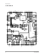
Page 105: ...PCB Diagrams 10 2 Samsung Electronics 10 1 Main COMPONENT SIDE SOLDER SIDE ...

Page 106: ...PCB Diagrams Samsung Electronics 10 3 10 2 Jack ...

Page 107: ...PCB Diagrams 10 4 Samsung Electronics 10 3 S M P S ...

Page 108: ...PCB Diagrams Samsung Electronics 10 5 10 4 Front COMPONENT SIDE SOLDER SIDE ...

Page 109: ...PCB Diagrams 10 6 Samsung Electronics 10 5 Key COMPONENT SIDE SOLDER SIDE ...

Page 110: ...PCB Diagrams Samsung Electronics 10 7 10 6 Head Phone 10 7 Deck COMPONENT SIDE SOLDER SIDE ...

Page 111: ...PCB Diagrams 10 8 Samsung Electronics 10 8 Sensor 10 9 Motor ...

Page 112: ...Samsung Electronics 11 1 11 Wiring Diagram JACK PCB DECK PCB MOTOR PCB SENSOR PCB HEAD PHONE PCB SWITCH PCB MAIN PCB S M P S PCB FRONT PCB KEY PCB ...

Page 113: ...Wiring Diagram 11 2 Samsung Electronics MEMO ...

Page 114: ... M P S 12 2 Main Power Supply 12 3 Main Micom 12 4 Servo 12 5 Video Encoder 12 6 Video 12 7 Audio DAC 12 8 Audio 12 9 RF 12 10 ZiVA 12 11 DSP 12 12 Front Micom VFD Display 12 13 Scart Jack Europe Only 12 14 Head Phone 12 15 Key 12 16 Deck 12 17 Deck Control 12 18 Remote Control Block Identification of PCB Main PCB Component Side Jack PCB Conductor Side ...

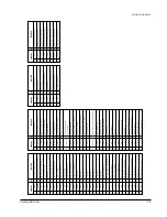
Page 115: ...Schematic Diagrams 12 2 Samsung Electronics 12 1 S M P S ...

Page 116: ...Schematic Diagrams Samsung Electronics 12 3 12 2 Main Power Supply ...

Page 117: ...Schematic Diagrams 12 4 Samsung Electronics 12 3 Main Micom ...

Page 118: ...Schematic Diagrams Samsung Electronics 12 5 12 4 Servo ...

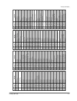
Page 119: ...Schematic Diagrams 12 6 Samsung Electronics 12 5 Video Encoder ...

Page 120: ...Schematic Diagrams Samsung Electronics 12 7 12 6 Video CVBS Output Y Output C Output ...

Page 121: ...Schematic Diagrams 12 8 Samsung Electronics 12 7 Audio DAC ...

Page 122: ...Schematic Diagrams Samsung Electronics 12 9 12 8 Audio ...

Page 123: ...Schematic Diagrams 12 10 Samsung Electronics 12 9 RF ...

Page 124: ...Schematic Diagrams Samsung Electronics 12 11 12 10 ZiVA ...

Page 125: ...Schematic Diagrams 12 12 Samsung Electronics 12 11 DSP ...

Page 126: ...Schematic Diagrams Samsung Electronics 12 13 12 12 Front Micom VFD Display ...

Page 127: ...Schematic Diagrams 12 14 Samsung Electronics 12 13 Scart Jack Europe Only B Output Scart Jack G Output Scart Jack R Output Scart Jack ...

Page 128: ...Schematic Diagrams Samsung Electronics 12 15 12 14 Head Phone ...

Page 129: ...Schematic Diagrams 12 16 Samsung Electronics 12 15 Key ...

Page 130: ...Schematic Diagrams Samsung Electronics 12 17 12 16 Deck ...

Page 131: ...Schematic Diagrams 12 18 Samsung Electronics 12 17 Deck Control ...

Page 132: ...Schematic Diagrams Samsung Electronics 12 19 12 18 Remote Control ...

Page 133: ...Schematic Diagrams 12 20 Samsung Electronics MEMO ...

Reviews: