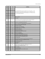

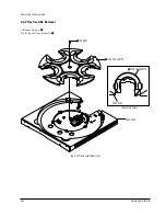
4-4
Samsung Electronics
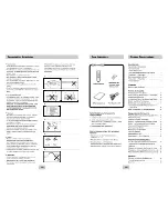
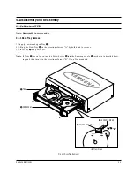
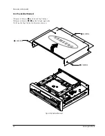
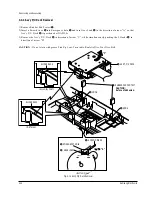
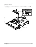
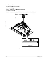
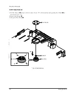
Disassembly and Reaasembly
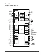
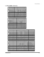
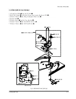
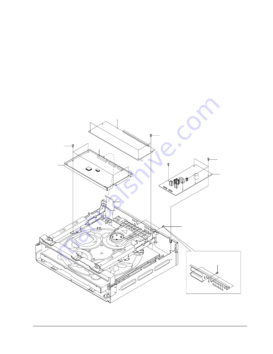
Œ
2 SCREWS (Black color)
; Region - America
´
3 SCREWS
ˇ
JACK PCB
¨
4 SCREWS
ˆ
MAIN PCB
”
S.M.P.S. PCB
Ø
4 SCREWS
∏
1 SCREW
(Black color ; 3x8)
FPC (Pin 36)
MCN06
Œ
4 SCREWS (Black color)
<Region - Europe>
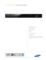
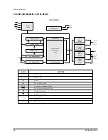
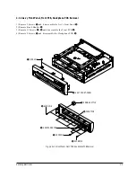
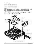
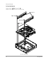
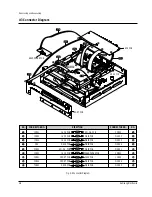
Fig. 4-4 Main PCB, Jack PCB, S.M.P.S. Removal
4-1-4 Main PCB, Jack PCB, S.M.P.S. Removal
1) Remove 2 Screws (4 Screws ; Region - Europe)
Œ
.
2) Remove 3 Screws
´
and lift the Jack PCB
ˇ
up.
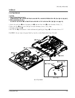
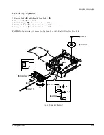
CAUTIONS ;
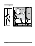
(1) When disassembling, switch the SW1 to “OFF” on the Deck PCB and remove the FPC connected to MCN06 on Main PCB.
(See Fig.1-4 on page 1-6)
(2) When assembling, insert the FPC into the MCN06 on Main PCB and switch SW1 to “ON” on the Deck PCB.
(See Fig.1-4 on page 1-6)
3) Disconnect FPC (Pin 36) from MCN06 on Main PCB
ˆ
, remove 4 Screws
¨
and lift the Main PCB
ˆ
up.
4) Remove 4 Screws
Ø
, 1 Screw
∏
and lift the S.M.P.S. PCB
”
up.
Summary of Contents for DVD-C700
Page 23: ...Reference Information 2 16 Samsung Electronics MEMO ...
Page 49: ...4 24 Samsung Electronics Disassembly and Reaasembly MEMO ...
Page 83: ...Troubleshooting 6 14 Samsung Electronics MEMO ...
Page 89: ...Exploded Views and Parts List 7 6 Samsung Electronics MEMO ...
Page 101: ...8 12 Samsung Electronics Electrical Parts List MEMO ...
Page 105: ...PCB Diagrams 10 2 Samsung Electronics 10 1 Main COMPONENT SIDE SOLDER SIDE ...
Page 106: ...PCB Diagrams Samsung Electronics 10 3 10 2 Jack ...
Page 107: ...PCB Diagrams 10 4 Samsung Electronics 10 3 S M P S ...
Page 108: ...PCB Diagrams Samsung Electronics 10 5 10 4 Front COMPONENT SIDE SOLDER SIDE ...
Page 109: ...PCB Diagrams 10 6 Samsung Electronics 10 5 Key COMPONENT SIDE SOLDER SIDE ...
Page 110: ...PCB Diagrams Samsung Electronics 10 7 10 6 Head Phone 10 7 Deck COMPONENT SIDE SOLDER SIDE ...
Page 111: ...PCB Diagrams 10 8 Samsung Electronics 10 8 Sensor 10 9 Motor ...
Page 113: ...Wiring Diagram 11 2 Samsung Electronics MEMO ...
Page 115: ...Schematic Diagrams 12 2 Samsung Electronics 12 1 S M P S ...
Page 116: ...Schematic Diagrams Samsung Electronics 12 3 12 2 Main Power Supply ...
Page 117: ...Schematic Diagrams 12 4 Samsung Electronics 12 3 Main Micom ...
Page 118: ...Schematic Diagrams Samsung Electronics 12 5 12 4 Servo ...
Page 119: ...Schematic Diagrams 12 6 Samsung Electronics 12 5 Video Encoder ...
Page 120: ...Schematic Diagrams Samsung Electronics 12 7 12 6 Video CVBS Output Y Output C Output ...
Page 121: ...Schematic Diagrams 12 8 Samsung Electronics 12 7 Audio DAC ...
Page 122: ...Schematic Diagrams Samsung Electronics 12 9 12 8 Audio ...
Page 123: ...Schematic Diagrams 12 10 Samsung Electronics 12 9 RF ...
Page 124: ...Schematic Diagrams Samsung Electronics 12 11 12 10 ZiVA ...
Page 125: ...Schematic Diagrams 12 12 Samsung Electronics 12 11 DSP ...
Page 126: ...Schematic Diagrams Samsung Electronics 12 13 12 12 Front Micom VFD Display ...
Page 128: ...Schematic Diagrams Samsung Electronics 12 15 12 14 Head Phone ...
Page 129: ...Schematic Diagrams 12 16 Samsung Electronics 12 15 Key ...
Page 130: ...Schematic Diagrams Samsung Electronics 12 17 12 16 Deck ...
Page 131: ...Schematic Diagrams 12 18 Samsung Electronics 12 17 Deck Control ...
Page 132: ...Schematic Diagrams Samsung Electronics 12 19 12 18 Remote Control ...
Page 133: ...Schematic Diagrams 12 20 Samsung Electronics MEMO ...