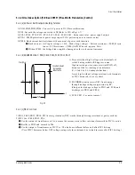
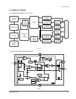
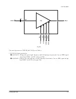
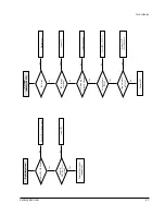
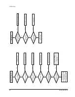

Circuit Descriptions
Samsung Electronics
5-13
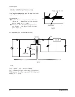
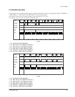
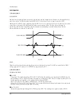
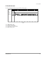
(2) SEARCH Mode :
Search mode : Fine seek,(Moving the tracking actuator slightly little below 255 track) and coarse search, moving
much in use of sled motor. The coarse search will be described in sled linked servo and now, the fine seek is
explained shortly.
If the object lens is located near target, cut off the tracking loop and give the control signal as many as desired
count to move the tracking actuator via SIC1 pin 76 terminal(TRD).
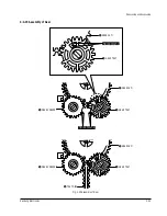
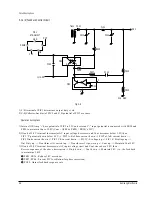
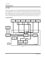
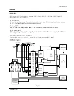
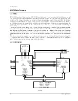
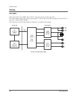
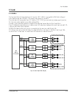
3) SLED LINKED SERVO
• Normal play mode
Move SLED motor slightly by means of PWM signal in SIC1 pin 73, as the tracking actuator moves along with
track during play. Control to move the entire Pick-up as the tracking actuator moves.
• Coarse serach mode
In case of long-distance search (such as chapter serach), SIC1 uses sled FG (SIC8 pin 1, 7, which is generated) by
rotation of sled motor via hall PCB. Then, read ID and compute the existing track count after input of next
track. If the existing track count is within fine seek range, tracking begins using fine seek.
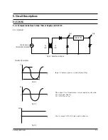
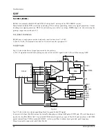
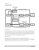
4) CLV SERVO(DISC MOTOR CONTROL SERVO)
Input RF signal (from Pick-up) to SIC1 pin59. Detect SYNC signal from RF in SIC1, and output PWM signal to
SIC1 pin 55 for constant linear velocity.
Summary of Contents for DVD-C700
Page 23: ...Reference Information 2 16 Samsung Electronics MEMO ...
Page 49: ...4 24 Samsung Electronics Disassembly and Reaasembly MEMO ...
Page 83: ...Troubleshooting 6 14 Samsung Electronics MEMO ...
Page 89: ...Exploded Views and Parts List 7 6 Samsung Electronics MEMO ...
Page 101: ...8 12 Samsung Electronics Electrical Parts List MEMO ...
Page 105: ...PCB Diagrams 10 2 Samsung Electronics 10 1 Main COMPONENT SIDE SOLDER SIDE ...
Page 106: ...PCB Diagrams Samsung Electronics 10 3 10 2 Jack ...
Page 107: ...PCB Diagrams 10 4 Samsung Electronics 10 3 S M P S ...
Page 108: ...PCB Diagrams Samsung Electronics 10 5 10 4 Front COMPONENT SIDE SOLDER SIDE ...
Page 109: ...PCB Diagrams 10 6 Samsung Electronics 10 5 Key COMPONENT SIDE SOLDER SIDE ...
Page 110: ...PCB Diagrams Samsung Electronics 10 7 10 6 Head Phone 10 7 Deck COMPONENT SIDE SOLDER SIDE ...
Page 111: ...PCB Diagrams 10 8 Samsung Electronics 10 8 Sensor 10 9 Motor ...
Page 113: ...Wiring Diagram 11 2 Samsung Electronics MEMO ...
Page 115: ...Schematic Diagrams 12 2 Samsung Electronics 12 1 S M P S ...
Page 116: ...Schematic Diagrams Samsung Electronics 12 3 12 2 Main Power Supply ...
Page 117: ...Schematic Diagrams 12 4 Samsung Electronics 12 3 Main Micom ...
Page 118: ...Schematic Diagrams Samsung Electronics 12 5 12 4 Servo ...
Page 119: ...Schematic Diagrams 12 6 Samsung Electronics 12 5 Video Encoder ...
Page 120: ...Schematic Diagrams Samsung Electronics 12 7 12 6 Video CVBS Output Y Output C Output ...
Page 121: ...Schematic Diagrams 12 8 Samsung Electronics 12 7 Audio DAC ...
Page 122: ...Schematic Diagrams Samsung Electronics 12 9 12 8 Audio ...
Page 123: ...Schematic Diagrams 12 10 Samsung Electronics 12 9 RF ...
Page 124: ...Schematic Diagrams Samsung Electronics 12 11 12 10 ZiVA ...
Page 125: ...Schematic Diagrams 12 12 Samsung Electronics 12 11 DSP ...
Page 126: ...Schematic Diagrams Samsung Electronics 12 13 12 12 Front Micom VFD Display ...
Page 128: ...Schematic Diagrams Samsung Electronics 12 15 12 14 Head Phone ...
Page 129: ...Schematic Diagrams 12 16 Samsung Electronics 12 15 Key ...
Page 130: ...Schematic Diagrams Samsung Electronics 12 17 12 16 Deck ...
Page 131: ...Schematic Diagrams 12 18 Samsung Electronics 12 17 Deck Control ...
Page 132: ...Schematic Diagrams Samsung Electronics 12 19 12 18 Remote Control ...
Page 133: ...Schematic Diagrams 12 20 Samsung Electronics MEMO ...