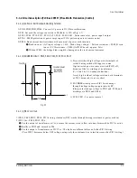
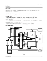
Circuit Descriptions
Samsung Electronics
5-17
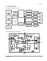
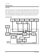
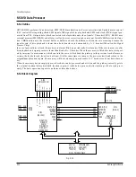
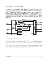
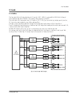
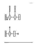
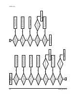
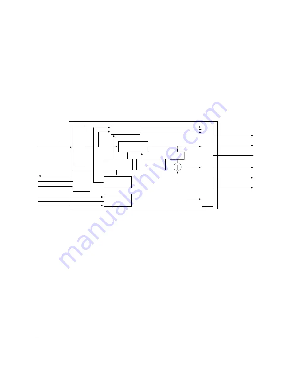
5-6-2 NTSC/PAL Digital Encoder (VIC50 : SAA7128)
VIC50 inputted from pin4 with 27MHz generates HSYNC and VSYNC which are based on video signal. Each
HSYNC and VSYNC outputted from Pin8 and Pin7 are inputted to Pin157 and Pin158 of A/V decoder VIC1(ZIVA-
3). VIC1 is the synchronous signals with the video signal and control the output timing of 8bit video signal of ITU-
R601 format. (Pin180, 182, 184 ~ 189 (MSP))
8bit data is inputted to Pin9(MSB) and Pin16 of VIC50 and the inputted data is demuxed with each 8bit of Y/R-Y/B-
Y. The separate signal is encoded to NTSC or PAL by control of MIC1. The above signals, that is CVBS
(Composite Video Burst Synchronized)(Pin30), S-Video (Y:Pin27, C:Pin24), Y/Pb/Pr(Pin27/Pin29/Pin23) and
GB(Pin26/Pin29/Pin23). In course of encoding, 8bit data can extend to 10bit or more. To convert the extended data
to quantization noise as possible, VIC50 adopts 10bit D/A converter. VIC50 perform video en-coding as well as
copy protection.
VDATA
[7:0]
VSYNC
HSYNC
27M
MRST
SDA
SCL
9~16
7
8
4
40
42
41
Demultiplexer
Y
CR-CB
RGB encoding
Luminace
processing
MACROVISION
7.0.1/6.1
Cloed captions
CGMS
Chrominance
processor
CTRL+CFG
register
Trap
10-bit DAC
30
27
24
23
26
29
CVBS
Y
C
Pr/R
G
Pb/B
VIC1 (SSA7128)
Fig. 5-22
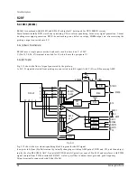
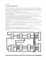
5-6-3 Amplifier (VIC51, VIC52 : BA7660)
VIC51 and VIC52 are 6dB amplifier. Based on CVBS signal, the final output level must be 2Vpp without 75ohm ter-
minal resistance. Because the level of video encoder output is only 1.1Vpp, the level is adjusted with the special
amplifier. When mute of pin1 is high active, if the pin is floating and connected to power, the output signal is never
outputted. CVBS, Y, C, Cr and Cb outputted from video encoder are inputted to VIC52 (Pin7, Pin2 and Pin4) and
VIC51 (Pin7 and Pin4) respectively and outputted from VIC52 (Pin10, Pin15 and Pin13) and VIC51 (Pin10 and Pin
13). Pin9, Pin12 and Pin14 of VIC51 and VIC52 are feedback pin to SAG compensation(DC characteristic compen-
sation of signal). Resistance(VR3-VR14) which is inserted to input terminal is bias resistance for input offset. The
signal to which gain is adjusted by amplifier is outputted from jack via 75ohm.
Summary of Contents for DVD-C700
Page 23: ...Reference Information 2 16 Samsung Electronics MEMO ...
Page 49: ...4 24 Samsung Electronics Disassembly and Reaasembly MEMO ...
Page 83: ...Troubleshooting 6 14 Samsung Electronics MEMO ...
Page 89: ...Exploded Views and Parts List 7 6 Samsung Electronics MEMO ...
Page 101: ...8 12 Samsung Electronics Electrical Parts List MEMO ...
Page 105: ...PCB Diagrams 10 2 Samsung Electronics 10 1 Main COMPONENT SIDE SOLDER SIDE ...
Page 106: ...PCB Diagrams Samsung Electronics 10 3 10 2 Jack ...
Page 107: ...PCB Diagrams 10 4 Samsung Electronics 10 3 S M P S ...
Page 108: ...PCB Diagrams Samsung Electronics 10 5 10 4 Front COMPONENT SIDE SOLDER SIDE ...
Page 109: ...PCB Diagrams 10 6 Samsung Electronics 10 5 Key COMPONENT SIDE SOLDER SIDE ...
Page 110: ...PCB Diagrams Samsung Electronics 10 7 10 6 Head Phone 10 7 Deck COMPONENT SIDE SOLDER SIDE ...
Page 111: ...PCB Diagrams 10 8 Samsung Electronics 10 8 Sensor 10 9 Motor ...
Page 113: ...Wiring Diagram 11 2 Samsung Electronics MEMO ...
Page 115: ...Schematic Diagrams 12 2 Samsung Electronics 12 1 S M P S ...
Page 116: ...Schematic Diagrams Samsung Electronics 12 3 12 2 Main Power Supply ...
Page 117: ...Schematic Diagrams 12 4 Samsung Electronics 12 3 Main Micom ...
Page 118: ...Schematic Diagrams Samsung Electronics 12 5 12 4 Servo ...
Page 119: ...Schematic Diagrams 12 6 Samsung Electronics 12 5 Video Encoder ...
Page 120: ...Schematic Diagrams Samsung Electronics 12 7 12 6 Video CVBS Output Y Output C Output ...
Page 121: ...Schematic Diagrams 12 8 Samsung Electronics 12 7 Audio DAC ...
Page 122: ...Schematic Diagrams Samsung Electronics 12 9 12 8 Audio ...
Page 123: ...Schematic Diagrams 12 10 Samsung Electronics 12 9 RF ...
Page 124: ...Schematic Diagrams Samsung Electronics 12 11 12 10 ZiVA ...
Page 125: ...Schematic Diagrams 12 12 Samsung Electronics 12 11 DSP ...
Page 126: ...Schematic Diagrams Samsung Electronics 12 13 12 12 Front Micom VFD Display ...
Page 128: ...Schematic Diagrams Samsung Electronics 12 15 12 14 Head Phone ...
Page 129: ...Schematic Diagrams 12 16 Samsung Electronics 12 15 Key ...
Page 130: ...Schematic Diagrams Samsung Electronics 12 17 12 16 Deck ...
Page 131: ...Schematic Diagrams 12 18 Samsung Electronics 12 17 Deck Control ...
Page 132: ...Schematic Diagrams Samsung Electronics 12 19 12 18 Remote Control ...
Page 133: ...Schematic Diagrams 12 20 Samsung Electronics MEMO ...