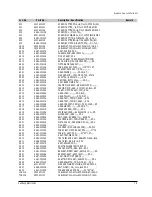
Troubleshooting
6-10
Samsung Electronics
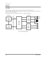
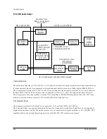
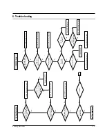
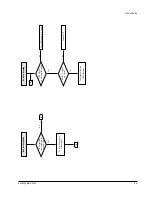
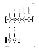
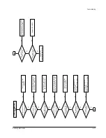
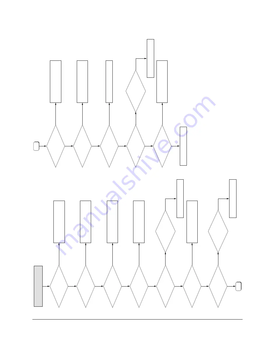
Video output error in
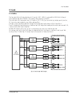
RCA Jacks
Power level is
normal at pin 6, 17, 20, 25, 28,
31, 36, 39 in VIC50?
27MHz clock input
is normal at pin 4 in
VIC50?
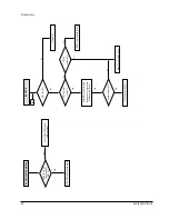
Check the connection between
pin 2 in PIC6 and Emmiter in PQ24.
Check the connection between
pin 10 in VIC6 and pin 4 in VIC50.
Yes
Yes
No
No
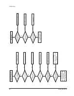
MRST is high state
at pin 40 in VIC50?
Yes
No
Control signal is
normal at pin 41, 42 in VIC50?
(When power on
or open)
Yes
No
SYNC signal is
normal at pin 7, 8 in
VIC50?
Check the soldering of VIC50.
Yes
Check the connection between
pin 1 in FIC1 and pin 40 in VIC50.
Check the connection between
pin 86, 87 in MIC1 and pin 41, 42 in VIC50.
Check the connection with
pin 180, 182, 184 ~ 189 in VIC1.
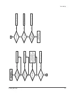
Video data are inputed
normally at pin 9 ~ 16 in
VIC50?
Analog signals output
normally at pin 30, 27, 24,
29, 23, in VIC50?
Yes
No
Yes
D
Change VIC50.
No
No
Check the soldering of VIC50.
Change VIC50.
No
No
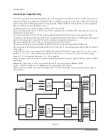
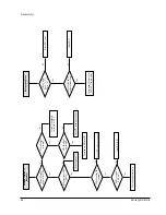
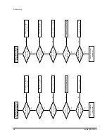
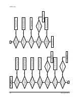
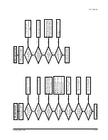
Analog signals
are inputed normally at pin 2, 4,
7 in VIC51, 52?
Power is normal
at pin 16 in VIC51, 52?
Check the connection between
VIC50 and VIC51, 52.
Check the connection between
VIC51, 52 and Emmiter of PQ24.
Yes
No
No
Pin 1 in VIC51, 52 is in
Low state?
Yes
No
Video signals of
about 2V appear at pin 10, 13, 15
in VIC51, 52?
Yes
No
Video signals of
about 1V appear at
output jacks?
Check the soldering of
VIC51, 52.
Yes
Connect to ground.
Check the connection between
VIC51, 52 and output jacks.
Check the RCA cable.
Yes
D
Change VIC51, 52.
No
No
Summary of Contents for DVD-C700
Page 23: ...Reference Information 2 16 Samsung Electronics MEMO ...
Page 49: ...4 24 Samsung Electronics Disassembly and Reaasembly MEMO ...
Page 83: ...Troubleshooting 6 14 Samsung Electronics MEMO ...
Page 89: ...Exploded Views and Parts List 7 6 Samsung Electronics MEMO ...
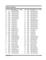
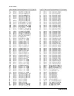
Page 101: ...8 12 Samsung Electronics Electrical Parts List MEMO ...
Page 105: ...PCB Diagrams 10 2 Samsung Electronics 10 1 Main COMPONENT SIDE SOLDER SIDE ...
Page 106: ...PCB Diagrams Samsung Electronics 10 3 10 2 Jack ...
Page 107: ...PCB Diagrams 10 4 Samsung Electronics 10 3 S M P S ...
Page 108: ...PCB Diagrams Samsung Electronics 10 5 10 4 Front COMPONENT SIDE SOLDER SIDE ...
Page 109: ...PCB Diagrams 10 6 Samsung Electronics 10 5 Key COMPONENT SIDE SOLDER SIDE ...
Page 110: ...PCB Diagrams Samsung Electronics 10 7 10 6 Head Phone 10 7 Deck COMPONENT SIDE SOLDER SIDE ...
Page 111: ...PCB Diagrams 10 8 Samsung Electronics 10 8 Sensor 10 9 Motor ...
Page 113: ...Wiring Diagram 11 2 Samsung Electronics MEMO ...
Page 115: ...Schematic Diagrams 12 2 Samsung Electronics 12 1 S M P S ...
Page 116: ...Schematic Diagrams Samsung Electronics 12 3 12 2 Main Power Supply ...
Page 117: ...Schematic Diagrams 12 4 Samsung Electronics 12 3 Main Micom ...
Page 118: ...Schematic Diagrams Samsung Electronics 12 5 12 4 Servo ...
Page 119: ...Schematic Diagrams 12 6 Samsung Electronics 12 5 Video Encoder ...
Page 120: ...Schematic Diagrams Samsung Electronics 12 7 12 6 Video CVBS Output Y Output C Output ...
Page 121: ...Schematic Diagrams 12 8 Samsung Electronics 12 7 Audio DAC ...
Page 122: ...Schematic Diagrams Samsung Electronics 12 9 12 8 Audio ...
Page 123: ...Schematic Diagrams 12 10 Samsung Electronics 12 9 RF ...
Page 124: ...Schematic Diagrams Samsung Electronics 12 11 12 10 ZiVA ...
Page 125: ...Schematic Diagrams 12 12 Samsung Electronics 12 11 DSP ...
Page 126: ...Schematic Diagrams Samsung Electronics 12 13 12 12 Front Micom VFD Display ...
Page 128: ...Schematic Diagrams Samsung Electronics 12 15 12 14 Head Phone ...
Page 129: ...Schematic Diagrams 12 16 Samsung Electronics 12 15 Key ...
Page 130: ...Schematic Diagrams Samsung Electronics 12 17 12 16 Deck ...
Page 131: ...Schematic Diagrams 12 18 Samsung Electronics 12 17 Deck Control ...
Page 132: ...Schematic Diagrams Samsung Electronics 12 19 12 18 Remote Control ...
Page 133: ...Schematic Diagrams 12 20 Samsung Electronics MEMO ...