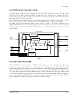
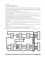
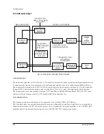

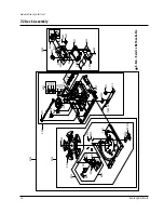

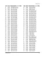
Troubleshooting
Samsung Electronics
6-11
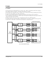
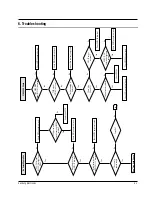
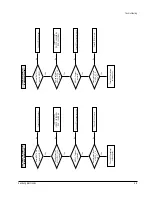
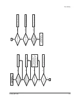
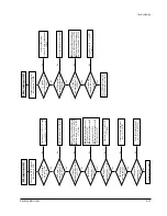
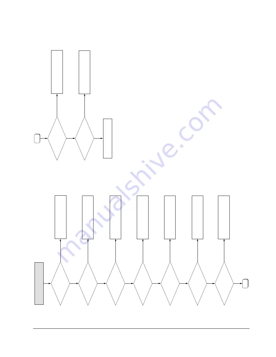
There is no output from
MIC
Is Karaoke mode on the
OSD display on?
Are the outputs of pin 2 of
MIC1 and 2 normal?
Turn on Karaoke mode
on the OSD.
Check the soldering around
jacks of Mic 1 and Mic 2.
Yes
Yes
No
No
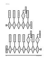
Are the outputs of pin 1 and
7 of KOP1 normal?
Yes
No
Does KVR1 (VR: 20K)
function normally?
Yes
No
Is the output of pin 1
of KOP2 normal?
Yes
Check power input of KOP1
and surrounding circuit.
Check the soldering and defect of
material around KVR1 (VR : 20K).
No
Check the surrounding
circuit of the KOP2.
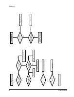
No
Check the input signal of
pin 4 of KCN1.
(DVD: 2.304MHz, CD: 2.116MHz)
Check the input signal of
pin 3 of KCN1.
(DVD: 48KHz, CD: 44.1 kHz)
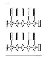
Is the input of pin 20
of KIC1 normal?
Is the input of pin 19
of KIC1 normal?
Yes
No
Yes
E
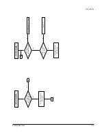
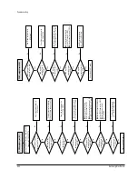
Is the input of pin 18
of KIC1 normal?
Is the input of pin 21
of KIC1 normal?
Check the input signal of pin 1 of KCN1.
(DVD: 18.432MHz, CD: 16.934MHz)
Replace KIC1 (AK5330)
Yes
No
No
Yes
Replace MIC8
(M27C801: MAIN MICOM)
E
Summary of Contents for DVD-C700
Page 23: ...Reference Information 2 16 Samsung Electronics MEMO ...
Page 49: ...4 24 Samsung Electronics Disassembly and Reaasembly MEMO ...
Page 83: ...Troubleshooting 6 14 Samsung Electronics MEMO ...
Page 89: ...Exploded Views and Parts List 7 6 Samsung Electronics MEMO ...
Page 101: ...8 12 Samsung Electronics Electrical Parts List MEMO ...
Page 105: ...PCB Diagrams 10 2 Samsung Electronics 10 1 Main COMPONENT SIDE SOLDER SIDE ...
Page 106: ...PCB Diagrams Samsung Electronics 10 3 10 2 Jack ...
Page 107: ...PCB Diagrams 10 4 Samsung Electronics 10 3 S M P S ...
Page 108: ...PCB Diagrams Samsung Electronics 10 5 10 4 Front COMPONENT SIDE SOLDER SIDE ...
Page 109: ...PCB Diagrams 10 6 Samsung Electronics 10 5 Key COMPONENT SIDE SOLDER SIDE ...
Page 110: ...PCB Diagrams Samsung Electronics 10 7 10 6 Head Phone 10 7 Deck COMPONENT SIDE SOLDER SIDE ...
Page 111: ...PCB Diagrams 10 8 Samsung Electronics 10 8 Sensor 10 9 Motor ...
Page 113: ...Wiring Diagram 11 2 Samsung Electronics MEMO ...
Page 115: ...Schematic Diagrams 12 2 Samsung Electronics 12 1 S M P S ...
Page 116: ...Schematic Diagrams Samsung Electronics 12 3 12 2 Main Power Supply ...
Page 117: ...Schematic Diagrams 12 4 Samsung Electronics 12 3 Main Micom ...
Page 118: ...Schematic Diagrams Samsung Electronics 12 5 12 4 Servo ...
Page 119: ...Schematic Diagrams 12 6 Samsung Electronics 12 5 Video Encoder ...
Page 120: ...Schematic Diagrams Samsung Electronics 12 7 12 6 Video CVBS Output Y Output C Output ...
Page 121: ...Schematic Diagrams 12 8 Samsung Electronics 12 7 Audio DAC ...
Page 122: ...Schematic Diagrams Samsung Electronics 12 9 12 8 Audio ...
Page 123: ...Schematic Diagrams 12 10 Samsung Electronics 12 9 RF ...
Page 124: ...Schematic Diagrams Samsung Electronics 12 11 12 10 ZiVA ...
Page 125: ...Schematic Diagrams 12 12 Samsung Electronics 12 11 DSP ...
Page 126: ...Schematic Diagrams Samsung Electronics 12 13 12 12 Front Micom VFD Display ...
Page 128: ...Schematic Diagrams Samsung Electronics 12 15 12 14 Head Phone ...
Page 129: ...Schematic Diagrams 12 16 Samsung Electronics 12 15 Key ...
Page 130: ...Schematic Diagrams Samsung Electronics 12 17 12 16 Deck ...
Page 131: ...Schematic Diagrams 12 18 Samsung Electronics 12 17 Deck Control ...
Page 132: ...Schematic Diagrams Samsung Electronics 12 19 12 18 Remote Control ...
Page 133: ...Schematic Diagrams 12 20 Samsung Electronics MEMO ...