62
5. PCB Diagrams
5. PCB Diagrams
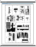
5-1 PCB Diagrams (Main)
(This Document can not be used without Samsung’s authorization)
ྙ
ྚ
ྜ
ྞ
ྜྷ
ྜྷ
ྟ
ྠ
ྡ
No.
Parts Number
Part Name
Function and Rule
1
C
N01
D
oor plunger switch, cooktop warming center
, oven lamp and relay of convection fan connector
T
his is connector which is con
nected with Door plunger switch and Door lock switch. (COM-NO, COM-NC)
2
C
N02
O
ven sensor Connector
This is connector which is connected with oven sensor
.
3
CN04, CN05
R
elay connector
This connector is to get all operating of relay on sub PCB to be connected.
4
C
N07
K
eypad Connector
This is consisted of 15 pin and take a role of getting a cable on keypad to connect with touch PCB.
5
CN08, CN09
A
T
erminal for connecting with SMPS Power Supply
This is to supply power with primary on Low voltage transformer
, and
AC120V with main PCB through
harness. It won
t be problem even though CN08 and CN09 has been changed when you insert housing.
6C
N
10
A
T
erminal for connecting with a small-sized RELA
Y
Power Supply
This is connector which take a role of supplying secondary voltage of Low voltage transformer with main
PCB.
7
Z
NR1
V
aristor
This is the element to protect main PCB, getting varistor to work if over voltage is supplied with varistor
.
8
IC02
DC 12V IC
This is to supply DC12V with main PCB by voltage regulator
.
9
IC03
DC 5V IC
This is to supply DC5V with main PCB by voltage regulator
.
1(5$%65B$$LQGE


