background image

Disassembly & Reassembly

Samsung Electronics

12-5

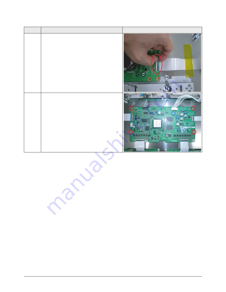
12-1-11 Separation of ASSY LOGIC BOARD

Part Name

Description

Description Photo

Flat Cable

Take care when separating the Logic Board not to damage 

the Flat-Cable Connector Cover.

Logic Board

Remove 4 screws.

: PH,+,WWP,M3,L8,NI PLT

Remove the Logic Board.

Summary of Contents for HPR4272X/XAC

Page 1: ...AY TV FEATURES NTSC ATSC Tuner Built In 12 Bit Processing 68 7 Billion Colors Split Screen Picture In Picture Samsung DNIe Digital Natural Image engine SRS TruSurround XT 1 HDMI Input Energy Saving An...

Page 2: ...is a property of Samsung Electronics Co Ltd Any unauthorized use of Manual can be punished under applicable International and or domestic law Samsung Electronics Co Ltd Jun 2005 Printed in Korea AA82...

Page 3: ...Service Mode 3 2 3 3 Factory Data 3 3 3 4 Service Adjustment 3 11 3 5 Software Upgrade 3 16 3 6 Replacements Calibration 3 18 Chapter 4 Exploded View Part List 4 1 HPR4272X XAC 4 1 Chapter 5 Electrica...

Page 4: ...3 Assy Side AV 10 13 Chapter 11 Operation Instruction Installation 11 1 Product Features and Functions 11 1 11 2 New Features 11 6 11 3 Installation Notes and Precautions 11 8 Chapter 12 Disassembly R...

Page 5: ...ut insulated transformers the product can only be repaired safely when the chassis is connected to the earthed end of the AC power source To make sure the AC power cord is properly connected follow th...

Page 6: ...placed with another irregular one the safety or protective features will be lost even if the new one has a higher voltage or more watts Critical safety parts should be bracketed with Use only regular...

Page 7: ...istance between the blade of the AC plug and that of the conductive material should be more than 1 7 Any B interlock should not be damaged If the metal heat sink is not properly installed no connectio...

Page 8: ...for soldering purposes 6 Use only anti static solder removal devices Most solder removal devices do not support an anti static feature A solder removal device without an anti static feature can store...

Page 9: ...sitioning the product Also check the antenna cable or the external connectors if they are fully unplugged Damage to the cord may cause fire or electric shock 6 Keep the antenna far away from any high...

Page 10: ...1 6 Samsung Electronics MEMO...

Page 11: ...22 Optical Coaxial Output Cabinet P5 Design New Cabinet Chip Description DNVD355BH401A Tuner ATSC NTSC QAM POD NIM Tuner STP22 Component CVBS Y C HDMI PC input Video signal processor SDP43 The DNIe IC...

Page 12: ...S VIDEO1 S VIDEO2 COMPONENT1 480i 480p 720p 1080i COMPONENT2 480i 480p 720p 1080i PC DVI AV Output AUDIO L R Speaker Output 15W 15W 8 Audio Output OPTICAL DIGITALOUT COAXIAL DIGITALOUT ETC DNIe Lite A...

Page 13: ...V PCM HDMI Feature Component Interface 480i 480p 720p 1080i Y Pb Pr Digital Interface HDMI 480p 720p 1080i Auto Program Sleep Timer 180 Minutes Anynet Interface My Color Control Color Weakness Energy...

Page 14: ...Horizontal Frequency KHz Vertical Polarity Horizontal Polarity IBM PC AT Compatible 640 X 350 70 086 31 469 P N 720 X 400 70 087 31 469 N P 640 X 480 59 940 31 469 N N 70 000 35 000 N P N P 72 809 37...

Page 15: ...thout Stand 87 7 Lbs Without Stand Picture Brightness 1 000 Cd m2 1 000 Cd m2 1 500 Cd m2 Contrast Ratio 3 000 1 3 000 1 10 000 1 Picture Enhacer DNIe 2 DNIe 3 DNIe Lite Comb Filter Audio Equalizer 5...

Page 16: ...8 00825G BN68 00825H Samsung Service center Remote Control AAA Batteries BN59 00462A 4301 000103 Power Cord 3903 000144 Anynet Cable BN39 00518A Accessories that can be purchased additionally S VIDEO...

Page 17: ...SMPS MAIN BN96 02213A Voltage Adjustment ASSY PCB P SMPS DC DC BN96 01856A Voltage Adjustment ASSY PCB P SMPS POD BN96 01805A ASSY PDP P LOGIC BOARD BN96 02035A ASSY PDP P X MAIN BOARD BN96 02032A ASS...

Page 18: ...ODE DISPLAY State T STRANUS0S 0036 and T STRANUS5 0117 are firmware version The firmware version is subject to change without notice 6 Buttons operations within Service Mode MENU Full Menu Display Mov...

Page 19: ...VCT Ver Check 0 V Chip Enable 1 Watchdog Enable 1 Spread Enable PC 1 Clock Adjust 4 Nim Version T310 MSP Version G New_WB_CbCr 1 ITEM Range Initial Values of Input Modes TV AV S video Component PC HD...

Page 20: ...0 255 120 120 120 120 02 TCD3 Brightness 0 255 49 49 49 49 03 TCD3 YC Delay 0 15 1 0 1 1 04 Analog Y Offset 0 1023 61 61 61 61 05 Analog PB Offset 0 1023 512 512 512 512 06 Analog PR Offset 0 1023 51...

Page 21: ...7 7 7 7 7 10 PeakTh2 P1 Luma Croma 0x16 7 0 0 255 2 2 2 2 0 0 2 2 2 11 PeakTh3 P1 Luma Croma 0x19 7 0 0 255 32 32 32 32 32 32 32 32 32 12 PeakN1Factor2 P1 Luma Croma 0x14 7 5 P1 Luma Croma 0x13 7 5 0...

Page 22: ...e 0 255 0x20 NICAM Prescale 0 255 0x20 AV Prescale 0 255 0x1C I2S_1 Prescale 0 255 0x10 I2S_3 Prescale 0 255 0x11 Carrier Mute 0 255 On Pilot High 0 255 0x0D Pilot Low 0 255 0x07 Scart1 Out Volume 0 2...

Page 23: ...White Balance Post 1 R Offset Post 512 511 0 0 0 0 2 G Offset Post 512 511 0 0 0 0 3 B Offset Post 512 511 0 0 0 0 4 R Gain Post 0 255 0 128 128 128 5 G Gain Post 0 255 0 128 128 128 6 B Gain Post 0...

Page 24: ...t 0 0 0 0 09 Standard Color 0 0 0 0 10 Standard Sharpness 0 0 0 0 11 Movie Contrast 12 Movie Bright 13 Movie Color 14 Movie Sharpness 15 RF_dB_1 Rf AV Noise Thres1 0 255 20 20 LowPassGain1 0 31 7 14 B...

Page 25: ...0 Test Pattern 01 OSD Pattern 01 Luma Ramp 32 Step 02 Luma Ramp 128 Step 03 White 16 04 White 240 05 Color Bar 06 RGB Ramp 32 Step 07 Cross Hatch 20X20 02 1 Channel Pattern 01 Y Filter 02 V PosGain 03...

Page 26: ...Line Range 0 1 1 02 Sound SD delay 0 2 1 03 Sound HD delay 0 2 1 04 Sound DTV delay 0 1 0 05 DDC Write 0 1 0 06 Auto Voltage Adj 5 07 Image Sticking 0 08 Error Mode Check 1 09 Error Code Table 4 10 Pa...

Page 27: ...pattern Use other equipment only after comparing the result with that of the Master equipment Set Aging Time Longer than 30 min Pattern Resolution Given below Calibration Available None and Pattern u...

Page 28: ...128 128 G Gain 128 128 128 128 128 B gain 128 128 128 128 128 R Cutoff 128 128 128 128 128 G Cutoff 128 128 128 128 128 B Cutoff 128 128 128 128 128 PC R Gain 128 128 128 128 128 G Gain 128 128 128 12...

Page 29: ...nal to the VIDEO IN port 3 Press the Source key to switch to AV S VIDEO mode 4 After confirming that the Lattice pattern appears select the Calibration menu 5 Select the AV Calibration menu 6 In AV Ca...

Page 30: ...the data c Adjust the low light Refer to Picture 2 3 for measurement point Adjust Sub Bright SVP to set the Y value Adjust red offset x and blue offset y to the color coordinates Do not adjust green...

Page 31: ...st white balance with 10 steps gray scale pattern of Picture 2 5 2 When you measure Low Light use 20 IRE portions And When you measure High Light use 70 IRE portion But if color noise is less in 60 IR...

Page 32: ...S 232 serial port and downloaded file If you want to change serial port you must edit bootdn bat and appdn bat bootdn bat sdn 1 0xdeadbbbb rom execution file file to be downloaded port number download...

Page 33: ...een Place the cursor over the On of Function Help and press the Info key on the remote control The version of the program is displayed at the bottom of the Menu screen 2 Procedures for checking in the...

Page 34: ...t 1 SMPS Panel voltages must be adjusted after changing SMPS PCB or PDP module Range Board Adjustment Vs 195 215V SMPS MAIN Va 50 70V Vset 180 210V SMPS DC DC Ve 70 110V Vscan 180 220V Voltage Label S...

Page 35: ...Alignment Adjustment Samsung Electronics 3 19 3 A point of adjusting SMPS DC DC Use base chassis of PDP panel as GND point...

Page 36: ...3 20 Samsung Electronics MEMO...

Page 37: ...BN96 02050A ASSY BOARD P POWER IR SCHUBERT CT5000 1 S A T0003 BN96 01773A ASSY COVER P FRONT 42P5 42S5 EXPORT 1 S A T0023 BN64 00336A KNOB POWER 42P5 PC VIOLET 1 S N A T0044 BN96 01886A ASSY PDP MODU...

Page 38: ...PDP P Y MAIN BOARD M1 SPD 42P5HD D7 1 S A T0124 BN96 02034A ASSY PDP P Y UPPER BUFFER BOAR M1 SPD 42 1 S A T0128 BN39 00518A CBF SIGNAL STEREO NA32KO 1P UL2464 26 20 1 S A T0142 BN96 02035A ASSY PDP...

Page 39: ...Samsung Electronics 5 2 MEMO...

Page 40: ...here is a burnt or damaged cable Check to see if there is a disconnected cable connection or a connection is too loose Check to see if the cables are connected according to the connection diagram 2 Ch...

Page 41: ...cables are improperly connected or the Video Board or SMPS is out of order In this case check the following Check the internal cable connection status inside the unit Check the fuses of each part Chec...

Page 42: ...and CN of the Y Drive Board a spark may be generated by the electric charge of the high capacity capacitor Therefore wait some time after separating the power cord from the unit Does the symptom conti...

Page 43: ...ating and connecting the cables such as CN809 of the Main SMPS CN1 CN2 CN3 CN4 and CN5 of the DC DC SMPS CN of the X Drive Board and CN of the Y Drive Board a spark may be generated by the electric ch...

Page 44: ...ing part of the Video Board is out of order Speaker defect Troubleshooting Procedures Is the cable connection between the main Board and the speaker properly connected Is the output voltage of SMPS no...

Page 45: ...Check the antenna connection settings Antenna 1 NTSC Cable 64QAM 256QAM Antenna 2 NTSC Air 8VSB ATSC Check the tuner output signal CVBS Check the power input of the Main board Troubleshooting Procedur...

Page 46: ...reen Screen noise 7 ASSY PDP P Y BUFF UPPER BOARD BN96 02034A Y Buffer Upper Board Upper screen is blank 8 ASSY PDP P Y BUFF LOWER BOARD BN96 02216A Y Buffer Lower Board Lower screen is blank 9 ASSY P...

Page 47: ...6 8 Samsung Electronics MEMO...

Page 48: ...Block Diagram Samsung Electronics 7 1 7 Block Diagram 7 1 Overall Block Diagram Y Main Board X Main Board 1024x768 Pixels 1024x768x3 Cells R G B 110V CPU Decoder Image Scaler Micom POD...

Page 49: ...lock Control and Switching Block Control and Switching Block Transformer Transformer Transformer Auxiliary Power Auxiliary Power Auxiliary Power Rectification Block Rectification Block Rectification B...

Page 50: ...amsung Electronics 7 3 7 2 3 Module Driver Board Block Diagram 1 Y Main Board Power Input Part Logic Signal Input Part Logic Signal Buffer 2 X Main Board Power Input Part Logic Signal Input Part Logic...

Page 51: ...POL STB R G B 16bit CLK A B BLK POL STB DATA 32bit ADDR 12bit DQS CLK nCLK RELAY_EINT AC OFF EINT Vs ON LVDS SIGNAL SDA SCL TX RX X MAIN CONTROL SIGNAL Y MAIN CONTROL SIGNAL ADC 4bit ADC 3bit ADC 1bi...

Page 52: ...ring Diagram Samsung Electronics 8 1 8 Wiring Diagram 8 1 Overall Wiring ASSY PCB MISC MAIN BN94 00694A ASSY POWER BN96 02050B ASSY SPEAKER BN96 01737A ASSY FUNCTION BN96 02049B ASSY SIDE AV BN94 0073...

Page 53: ...DC DC SMPS CN5007 Y B D Pin No Signal 1 Vs 2 Vs 3 RTN 4 RTN 5 Vset 6 RTN 7 Vscan 8 RTN 9 Vg 10 5 3V CN4 DC DC SMPS CN4004 X B D Pin No Signal 1 Vs 2 Vs 3 RTN 4 RTN 5 Ve 6 RTN 7 RTN 8 Vg 9 5 3V CN5 DC...

Page 54: ...B D CN2077 LOGIC B D Pin No Signal Pin No Signal Pin No Signal 1 12 TXOUT3 23 TXOUT1B 2 GND 13 TXOUT3 24 TXOUT1 3 PW_SDA0 14 TXCLKOUTB 25 TXOUT1 4 GND 15 TXCLKOUTB 26 GND 5 PW_SCL0 16 TXCLKOUT 27 GND...

Page 55: ...5 RTN 6 12V 7 RTN 8 6 5V 9 RTN 10 5V 11 RTN 12 5V CN101 MAIN B D SIDE AV Pin No Signal 1 VIDEO2_CVBS 2 GND 3 VIDEO2_IDENT 4 SVHS2_IDENT 5 VIDEO2_SL_IN 6 GND 7 VIDEO2_SR_IN 8 GND 9 SVHS2_Y 10 GND 11 SV...

Page 56: ...C PAL 42 INCH LJ92 01199A 5 ASSY PDP P Y MAIN BOARD BN96 02033A M1 SPD 42P5HD D71A V4 1002x590 1024x768 NTSC PAL 42 INCH LJ92 01200A 6 ASSY PDP P Y BUFF UPPER BOARD BN96 02034A M1 SPD 42P5HD D71A V4 1...

Page 57: ...9 2 Samsung Electronics MEMO...

Page 58: ...O V 2 3 D N G N I V 4 5 V 0 1 L T M W K 6 0 0 3 I S 9 0 0 1 C I m h o 0 8 3 0 1 R F u 7 4 3 3 0 1 C 0 2 0 1 R m h o K 0 1 1 A B 2 m h o 0 0 1 1 0 0 1 R 4 5 6 7 8 S 0 0 6 P 1 4 M L B 2 1 0 1 D B W 6 1...

Page 59: ...1 0 2 R m h o 0 5 1 1 4 0 1 2 R F n 0 0 1 4 1 1 2 C F E R X F E R X W 0 1 1 3 2 1 2 R m h o K 0 0 1 1 _ 1 _ V 3 3 B 3 0 1 2 R 1 Q 7 6 1 8 1 D 8 9 1 Q 8 0 1 D N G 2 Q I 1 1 H C T A L 1 T U P T U O 0 2...

Page 60: ...N I 2 T 6 0 0 3 C I E W C E 2 3 2 X A M 1 1 C 3 1 0 3 D m h o 5 7 1 2 1 3 R m h o 0 0 1 2 8 Z L R 9 2 1 3 R 8 2 0 3 R 6 2 0 3 R F E R X m h o 0 0 2 0 3 C m h o 0 1 0 0 3 P O 0 7 8 2 0 0 0 5 T C 1 2 3...

Page 61: ...4 7Kohm 3 1 0 4 D 3 3 0 4 D 1 1 E T B 6 5 Z L R R4081 R4081 m h o K 7 2 1 0 0 4 R 1 m h o 0 0 1 8 2 0 4 R 5 6 7 8 9 0 1 8 0 0 4 P T 2 0 0 4 A J L A V L P U S 4 3 0 0 4 L R4039 R4039 22ohm 22ohm F E R...

Page 62: ...3 3 B V 3 3 A V 6 1 F u 0 1 5 2 0 5 C F n 0 0 1 R5027 R5027 33ohm 33ohm V 6 1 F u 2 2 R5041 R5041 33ohm 33ohm 1 1 1 5 C F E R X 5 6 0 5 C F n 0 0 1 6 0 1 5 C 0 7 0 5 R 1 _ 1 _ V 3 3 B F E R X m h o 0...

Page 63: ...1 0 6 D A 1 V 0 5 1 7 3 0 6 R m h o K 7 4 1 4 0 0 6 C N 3 2 0 6 D A 1 5 0 0 6 C N V 5 A 4 7Kohm R6023 R6024 4 7Kohm D G S 2 _ V 3 3 B L 2 0 0 7 N 2 2 0 0 6 Q 2 0 0 6 C F u 0 0 1 V 6 1 V 6 1 8 4 0 6 C...

Page 64: ...8 1 D A 1 A B M 0 2 C A 8 2 A T A D M 1 2 C A 3 M Q D M 2 2 C A 1 2 A T A D M 4 2 C A 8 1 A T A D M 5 2 C A 4 1 A T A D M 6 2 C A 8 A T A D M 7 C A 0 6 A T A D M 8 C A 6 5 A T A D M 7 2 A T A D M 1 2...

Page 65: ...F E R X m h o K 7 4 8 1 0 8 R W 0 1 1 V 6 1 8 0 0 8 C F n 0 0 1 F E R X m h o 0 0 1 3 1 0 8 R F u 0 1 8 4 0 8 C F n 0 0 1 0 3 0 8 C V 0 5 6 4 0 8 C F u 0 1 1 D 1 7 4 8 4 E L 1 3 Q 1 5 4 Q 1 6 7 C C V...

Page 66: ...I_G_DIN01 I_G_DIN01 46 46 47 47 I_G_DIN00 I_G_DIN00 VDD4 VDD4 48 48 N I _ C N Y S V _ I N I _ C N Y S H _ I 5 3 9 1 D D V 6 3 9 0 N I D _ G _ I 7 3 8 0 N I D _ G _ I 8 3 7 0 N I D _ G _ I 9 3 2 0 N I...

Page 67: ...06 1 M 2 5 0 4 C H 4 7 M M 1 0 1 C I m h o K 3 3 TP105 SUPLVAL 1 SUPLVAL 8 2 1 R 3 0 1 L 4 0 1 D 2 8 Z L R F p 0 3 3 5 0 1 C 2 8 Z L R 9 0 1 D 1 1 1 D 2 8 Z L R 2 8 Z L R 0 1 1 D 2 8 Z L R F n 0 0 1 1...

Page 68: ...Schematic Diagram 10 11 Samsung Electronics 10 11 Function A ssy Board This Document can not be used without Samsung s authorization...

Page 69: ...6 1 ZD001 BZX84C5V1 1 2 3 ZD002 BZX84C5V1 1 2 3 ZD003 BZX84C5V1 1 2 3 0 0 1 8 0 6 1 7 0 0 R 0 0 1 8 0 6 1 8 0 0 R C002 1608 100nF C003 1608 100nF C004 1608 5pF C005 1608 5pF C006 1608 5pF 1 0 0 W S M...

Page 70: ...Schematic Diagram 10 13 Samsung Electronics 10 13 Assy Side AV This Document can not be used without Samsung s authorization...

Page 71: ...U button Displays the main on screen menu 3 VOL buttons Press to increase or decrease the volume Also used to select or adjust items on the on screen menu 4 CH buttons Press CH or CH to change channel...

Page 72: ...L R Video Input S Video Input Ferrite Cores The ferrite cores are used to attenuate undesired signals When connecting cables attach one of these ferrite cores to the cable near the connector When you...

Page 73: ...ck on your PC 6 PC AUDIO IN Connect to the audio output jack on your PC 7 OPTICAL DIGITAL AUDIO OUT Connect to a Digital Audio component 8 COAXIAL DIGITAL AUDIO OUT Connect to a Digital Audio componen...

Page 74: ...the Anynet view functions and sets up Anynet devices 9 MENU button Displays the main on screen menu 10 ENTER button Confirms a selection 11 FAV CH button Press to switch to your favorite channels 12...

Page 75: ...ate Audio Program SAP broadcast 26 SET button Used during set up of this Samsung remote control so that it will work compatibly with other devices VCR Cable Box and DVD 27 PIP button Activates picture...

Page 76: ...he PDP panel thus reducing power consumption Procedures for entering the menu Select Menu Setup Energy Saving Mode When pressing the Energy Saving Mode button on the remote control The Energy saving m...

Page 77: ...ate Note This TV has only one tuner and does not allow you to watch one TV channel in the main screen and another channel in the PIP screen Main screen PIP screen TV AV A S Video A Component A PC HDMI...

Page 78: ...y damage to the product or injury to yourself or others if you elect to perform the wall installation 3 This product is for installing on cement walls The product may not stay in place when installed...

Page 79: ...ct If the length is too short or long loosen all or some of the 4 screws on the wall bracket to adjust the length Hinge Left Length between the two locking holes Captive Screws Hinge Right 3 Check the...

Page 80: ...the 4 product holders into the corresponding bracket holes Then place the product so that it is firmly fixed to the bracket Make sure to reinsert and tighten the safety pin to securely hold the produ...

Page 81: ...el brackets are tightened Otherwise the TV panel may fall down Please secure the mounting bracket on the wall surface after setting its angle at 0 Note Note Adjust the bracket angle to 2 o before inst...

Page 82: ...the floor because of possible damage to the screen Always store the TV upright 1 Using the 4 screws for securing the stand pegs and the monitor firmly attach the monitor to the stand pegs The exterior...

Page 83: ...ble is longer than for normal use check the visual quality of the video on the screen and shorten the length if necessary This also applies to the PC RGB D Sub cable When the length of the cable is lo...

Page 84: ...r or game console through a wide TV by selecting the aspect ratio to normal 4 3 or wide 21 9 the left and right or top and bottom of the picture will not be displayed This symptom appears in other man...

Page 85: ...g is a television broadcasting signal digitized and transmitted according to the United States terrestrial digital broadcast standard or ATSC Mono A type of audio interface that transmits the audio si...

Page 86: ...rovide clearer and sharper visual quality Anynet Anynet is an AV network system that enables an easy to use AV interface for users by controlling all connected AV devices through the Anynet menu when...

Page 87: ...ree primary colors of light R G and B the number of possible colors for a pixel is 256 x 256 x 256 16 777 216 or 16 7 million colors If 12 bits are used for a pixel the gradation is 212 or 4096 for a...

Page 88: ...of the signal broadcast from a broadcast station is smaller than that of possible color coordinates Moreover a TV provides a smaller color coordinate area than that of the signal from the broadcastin...

Page 89: ...f t e s e r r o s s e c o r p c e S m 0 7 c e S m 0 7 N O r e l l o r t n o C e t o m e R N O r e l l o r t n o C e t o m e R N O r e l l o r t n o C e t o m e R N O r e l l o r t n o C e t o m e R S...

Page 90: ...NSP 6241A Sound PWM IC 10 IC2015 TAS5122 Sound AMP IC 11 IC3002 3F866B Generates various control signals required for operating the circuit The software is downloaded through PC D SUB Jack 12 IC3003 P...

Page 91: ...ut S Video SPK out CN2001 FAN Conn CN8001 MAIN OOB OOB MAIN SUB 1 POD_SW 2 3 GND 4 S_12V 5 GND 6 S_12V 7 GND 8 S_6 5V 9 GND 10 S_5V 11 GND 12 S_5V 1 FAN_D 2 THER_D 3 STD_5V 4 GND 5 PS_ON 6 D12V 7 GND...

Page 92: ...ion 1 RM01 Remote Control Sensor 2 SW001 Power Button 3 OP001 The Illumination sensor that senses the quantity of light It senses the illumination and automatically adjusts the screen brightness accor...

Page 93: ...6 12V 7 RTN 8 RTN 9 VCA 10 VCS 11 RTN 12 5 3V 3 CN803 MAIN SMPS CN1001 MAIN B D Pin No Signal 1 RTN 2 VT 33V 3 RTN_AMP 4 RTN_AMP 5 18V_AMP 6 18V_AMP 7 RTN 8 12V 9 RTN 10 6V 4 CN810 Main SMPS CN2004 Lo...

Page 94: ...or PDP 42inch The output voltage and current requirements for continu ous operation are stated below Table 1 Table 1 Specification of Output Power Supplies for PDP SMPS 4 Over Voltage Protection The o...

Page 95: ...3 above Current Protection as defined below Table 3 Table 3 Over Current Protection 6 Function of Board Remote Control Using a 250VAC 10A relay The board makes remote control available Protection The...

Page 96: ...charged by Vref through Rt and discharged by an internal current source During change time the internal clock signal blanks the output to the low state Selection of Rt and Ct therefore determines both...

Page 97: ...Circuit Description Samsung Electronics 13 9 Output VA Multi Outputs Pulse VA Main Pulse Multi Outputs Main Pulse...

Page 98: ...ck regulator U605 6 5V Buck regulator U604 KIA278R12 12V 2A KEC 12V regulator U401 KA3845 30V 1A FAIRCHILD VS PWM IC BD101 D15XB60 600V 15A SHINDENGEN Bridge diode D406 D407 D411 D412 RHR15120 1200V 1...

Page 99: ...cs 13 11 13 2 7 POD SMPS 1 J0802 POD SMPS CN8002 MAIN B D Pin No Signal 1 N C 2 33V 3 GND 4 12V 5 GND 6 12V 7 GND 8 6 5V 9 GND 10 5V 11 GND 12 5V 2 J0802 POD SMPS CN811 MAIN SMPS Pin No Signal 1 AC 2...

Page 100: ...the electrolytic capacitor C805 to the secondary coil T801 MAIN TRANS by turning the MOS FET embedded in U802 5M0565R on or off for PWM power and generates a DC output voltage of 5 3V 6 5V 12V and 30...

Page 101: ...l 1 5 3V 2 Vg 3 RTN 4 RTN 5 RTN 6 RTN 7 RTN 8 Va 9 Va 10 N C 11 Vs 12 Vs DC DC SMPS 4 CN1 N A 5 CN5 CN2601 F Buffer Pin No Signal 1 RTN 2 N C 3 5 3V 4 N C 5 Va 2 CN2 DC DC SMPS CN5003 Y B D Pin No Sig...

Page 102: ...ary Power Rectification Block Rectification Block Rectification Block Feedback Block Feedback Block Feedback Block Vs Input Part 205V 195 215 Vscan Output 198V 180 220 Vset Output 198V 180 210 Ve Outp...

Page 103: ...MAIN BOARD BN96 02032A X Drive Board 3 ASSY PDP P Y MAIN BOARD BN96 02033A Y Drive Board 4 ASSY PDP P ADDRESS E BUFFER BOARD BN96 02036A Address Buffer Board 5 ASSY PDP P ADDRESS F BUFFER BOARD BN96...

Page 104: ...1Pin LVDS SPS NIRB ASIC 816P DDR FA DDR MA DDR MB MICOM DRIVE RESET R G B 16bit CLK A B BLK POL STB R G B 16bit CLK A B BLK POL STB DATA 32bit ADDR 12bit DQS CLK nCLK RELAY_EINT AC OFF EINT Vs ON LVDS...

Page 105: ...SIC CHIP The main processor that generates and outputs the logic drive signal and the address data MICOM LOADING 5PIN CONNECTOR Debug only The connector to load the Micom drive program The program is...

Page 106: ...t the output waveform is normal using an oscilloscope Check if the waveform is the same as shown in Figure 2 by connecting the oscilloscope to the No 12 TP in Figure 1 Check if the waveform is the sam...

Page 107: ...That is the pixel whose wall charge has been formed by the Address Discharge forms a Sustain Discharge vis the following Sustain pulse 2 Sustain Discharge A Sustain Discharge is a Self Sustaining Dis...

Page 108: ...Operation Power Supplied from the power board The optimal value may differ from the following a Vs 205V Sustain b Vset 195V Y Rising Ramp c Ve 100V Ve bias d Vscan 190V Scan low bias e Vnf 175V Y fal...

Page 109: ...and 2 Ve bias in the Scan section is maintained 2 Y Drive Board This is connected to the Y port part of the panel It outputs 1 Sustain voltage wave form including ERC and 2 Y Rising Falling Ramp wave...

Page 110: ...PC output electrodes sequentially one line at a time At this time Vscan is called the Scan Bias Voltage A Vscan voltage of approximately 175 Volt Vsc_1 is supplied to the electrode lines For the other...

Page 111: ...nce 0 2 When no signal is output to the gate GND FET changes to an open circuit i e an insulator of resistance High Voltage Switching of the FET Operation 1 When no signal is applied to G1 FET1 is ope...

Page 112: ...Description 13 24 Samsung Electronics Drive Board Connector Layout 1 X Main CN4003 Signal CN4004 Power 1 D5 3V 2 Vg 3 RTN 4 RTN 5 Ve 6 RTN 7 RTN 8 Vs 9 Vs 120mm 310mm CN4000 Panel CN4002 Panel CN4001...

Page 113: ...in 1 Vs 2 Vs 3 RTN 4 RTN 5 Vset 6 RTN 7 Vscan 8 RTN 9 Vg 10 D5 3V CN5003 Powr CN5004 Signal CN5402 Panel 310mm 165mm CN5403 Panel CN5401 Panel CN5501 Panel CN5502 Panel CN5503 Panel CN5006 CN5001 CN50...

Page 114: ...e Y Main board Check OUTL and OUTH and confirm that the forward voltage reduction is between 0 4V 0 5V UP CN5407 1 10pin OUTH 11 33pin OUTL LOW CN5507 50 41pin OUTH 40 17pin OUTL In addition the resis...

Page 115: ...amsung Electronics 13 27 2 Y Main Connect the Y Main and Y Buffer and confirm that the output from TP CN5410 CN5411 of the Y Buffer UP is the same as Attachment 1 when the power is supplied TP Line383...

Page 116: ...tion 13 28 Samsung Electronics 3 X Main Check that the output of X Out of the X board follows the waveform of Attachment 2 when the power is supplied CN4001 Panel CN4002 Panel CN4000 Panel CN4003 Sign...

Page 117: ...Circuit Description Samsung Electronics 13 29 Attachment 1 Y Output Waveform The Scan Waveform Must Be Observed Y Output Waveform 200us div 100V div 1us div 100V div Sustain Waveform...

Page 118: ...Circuit Description 13 30 Samsung Electronics Attachment 2 X Output Waveform X Output Waveform 200us div 100V div 2us div 100V div Sustain Waveform...

Page 119: ...550 and is currently being used in LCD TVs It also uses SMBUS which is the same type as I2C for communication The Ambient Light Sensor can detect up to 1846 Lux in normal mode The data of the sensor c...

Page 120: ...mber of sustain pulses according to the ASL Average Signal Level by R_P_Lower_Gain value In the PDP Logic R_Multi_APC is set to 0X01 Multi_APC operates and R_P_CM_Gain_SW is set to 0X01 so that the up...

Page 121: ...eparation of ASSY COVER STAND CABLE Notice Be sure to separate the power cord before disassembling the unit Discharge the capacitors first when separating PCB s with high capacity capacitors such as S...

Page 122: ...BLK Remove the 2 Hex nuts for the PC input M3 L6 NI PLT SUM24L 4 40 Remove the cover rear 12 1 4 Separation of ASSY COVER P REAR Part Name Description Description Photo Rear Remove 22 screws BH S M4 L...

Page 123: ...nics 12 3 12 1 6 Separation of ASSY PCB MISC MAIN Part Name Description Description Photo Main Board Remove 5 screws PH WWP M3 L8 NI PLT Remove all connectors from the board Remove the Main Board 12 1...

Page 124: ...ASSY SMPS DC DC PCB then remove the board Wear gloves when handling the power board as there may be some remaining electrical charge in the capacitor Specifically avoid touching any part of the capac...

Page 125: ...12 1 11 Separation of ASSY LOGIC BOARD Part Name Description Description Photo Flat Cable Take care when separating the Logic Board not to damage the Flat Cable Connector Cover Logic Board Remove 4 sc...

Page 126: ...d To separate the Flat Cable of the X Board press the upper and the lower sides of the connector While pressing the connector apply slight force toward the direction of the cable to release the connec...

Page 127: ...d connectors from the Panel Assy by pulling the holder from both the top and bottom ends Y Scan Remove 2 screws PH WWP M3 L8 NI PLT Connectors Separate the Scan Boards from the Y Main Board by detachi...

Page 128: ...acket Remove 8 screws BH S M4 L8 ZPC BLK Separate PDP module from Front cover Please lay the PDP panel face down on a soft surface when separating front cover Remove 16 screws BH S M4 L10 ZPC BLK TCP...

Reviews: