background image

Troubleshooting

4-8

Samsung Electronics

Condition Name

Description

Related Board

No Voltage Output

Operating Voltage don't exist

PSU

No Display

Operating Voltage exist, but an Image doesn't exist on screen Y-MAIN, X-MAIN, Logic Main, Cable

Abnormal Display

Abnormal Image (not open or short) is no screen

Y-MAIN, X-MAIN, Logic Main

Sustain Open

Some horizontal lines don't exist on screen

Scan Buffer, FPC of X/Y

Sustain Short

Some horizontal lines appear to be linked on screen

Scan Buffer, FPC of X/Y

Address Open

Some vertical lines don't exist on screen

Logic Main, Logic Buffer, TCP

Address Short

Some vertical lines appear to be linked on screen

Logic Main, Logic Buffer, TCP

"

"

Drive Board Troubleshooting

1) Troubleshooting Summary

Summary of Contents for HPT4254 - 42" Plasma TV

Page 1: ...ssembly Reassembly 4 Troubleshooting 5 Exploded View Part List 6 Wiring Diagram 7 Schematic Diagram 0 12314 HP T4254 HP T5054 5166768 9 74A BCD4 8 EF GHG FIF GHG Refer to the service manual in the GSPN see the rear cover for the more information ...

Page 2: ...stic law Samsung Electronics Co Ltd Feb 2007 Printed in Korea AA82 04340A Area Web Site North America service samsungportal com Latin America latin samsungportal com CIS cis samsungportal com Europe europe samsungportal com China china samsungportal com Asia asia samsungportal com Mideast Africa mea samsungportal com GSPN Global Service Partner Network ...

Page 3: ...sories 2 4 Chapter 3 Disassembly Reassembly 3 1 Overhaul Disassembly Reassembly 3 1 Chapter 4 Troubleshooting 4 1 Troubleshooting 4 1 4 2 Adjustment 4 16 4 3 Upgrade 4 33 Chapter 5 Exploded View Part List 5 1 HPT4254X XAA Exploded View 5 1 5 2 HPT5054X XAA Exploded View 5 3 5 3 HPT4254X XAA Service Item 5 5 5 4 HPT5054X XAA Service Item 5 6 Chapter 6 Wiring Diagram 6 1 Overall Wiring 6 1 Chapter 7...

Page 4: ...insulated transformers the product can only be repaired safely when the chassis is connected to the earth end of the AC power source To make sure the AC power cord is properly connected follow the instructions below Use the voltmeter to measure the voltage between the chassis and the earth ground If the measurement is over 1 0V unplug the AC power cord and change the polarity before re inserting i...

Page 5: ...eplaced with another irregular one the safety or protective features will be lost even if the new one has a higher voltage or more watts Critical safety parts should be bracketed with Use only regular parts for replacements in particular flame resistance and dielectric strength specifications Irregular parts or materials may cause electric shock or fire Precaution 1 2 Samsung Electronics ...

Page 6: ...istance between the blade of the AC plug and that of the conductive material should be more than 1 7 Any B interlock should not be damaged If the metal heat sink is not properly installed no connection to the AC power should be made 8 Make sure the grounding lead of the tester is connected to the chassis ground before connecting to the positive lead The ground lead of the tester should be removed ...

Page 7: ...ns for soldering purposes 6 Use only anti static solder removal devices Most solder removal devices do not support an anti static feature A solder removal device without an anti static feature can store enough static electricity to cause damage to the ESD 7 Do not remove the ESD from the protective box until the replacement is ready Most ESD replacements are covered with lead which will cause a sh...

Page 8: ...ositioning the product Also check the antenna cable or the external connectors if they are fully unplugged Damage to the cord may cause fire or electric shock 6 Keep the antenna far away from any high voltage cables and install it firmly Contact with the high voltage cable or the antenna falling over may cause fire or electric shock 7 When connecting the RF antenna check for a DTV receiving system...

Page 9: ...1 6 Samsung Electronics MEMO ...

Page 10: ...cation Model HP T4254 HP T5054 Screen Size 42 Inches 16 9 50 Inches 16 9 Dimensions WxHxD 41 5 x 29 9 x 12 4 inches 48 4 x 33 4 x 12 4 inches Weight 73 2 lbs 33 2 kg 97 lbs 44 kg PC Resolution 1024 x 768 75Hz 1365 x 768 60Hz Voltage AC 100 240V 60Hz ANTENNA input ANT 1 AIR IN ANT 2 CABLE IN 75 unbalanced VIDEO input AV1 AV2 S VIDEO1 S VIDEO2 COMPONENT1 480i 480p 720p 1080i COMPONENT2 480i 480p 720...

Page 11: ...me Theater You can listen to 5 1 channel sound through the home theater s speakers Otherwise you can only listen to 2 channel stereo sound in other cases Make sure to connect the Digital Audio IN Optical of the home theater and the TV correctly to listen to TV sound through the home theater However you cannot listen to sound from the BD recorder that is sent to the home theater via the TV in 5 1 c...

Page 12: ... Ratio 10000 1 10000 1 7 000 1 Picture Enhacer FBE2 FBE2 LBE Comb Filter Audio Equalizer 5 Band 5 Band 5 Band Auto Volume Control Surround Sound SRS TruSurround XT SRS TruSurround XT SRS TruSurround XT Dolby Digital AC3 Speaker Output 10W 10W 15W 15W 10W 10W Features PIP Double Window Caption Still Image EPG My Color Control Color Weakness X X Energy Saving Anynet X Connections Antenna 2 Cable Air...

Page 13: ...Manual BN68 00872A AA68 03870B AA68 03242F Cloth Clean BN63 01798A Ferrite Core for Power Cord 3301 001110 Ferrite Core for Side AV S VIDEO 3301 001305 Ferrite Core for Headphone 3301 001456 Cover Bottom Screws 2ea BN63 03055A 6003 001621 Accessories that can be purchased additionally S VIDEO Cable 47 244 inches BN39 00149A Electronics Store Internal shopping mall HDMI Cable 118 11 inches BN39 006...

Page 14: ...ssories Item Item code Remark Accessories that can be purchased additionally Optical Cable None Electronics Store Internal shopping mall PC Cable 72 047 inches BN39 00115A PC Audio Cable 78 740 inches BN39 00061B Antenna Cable 118 11 inches BN39 00333A ...

Page 15: ...2 6 Samsung Electronics MEMO ...

Page 16: ...ge the capacitors first when separating PCB s with high capacity capacitors such as SMPS X Main Board Y Main Board etc A spark may be generated by the electric charge and there is danger of electronic shock Check that the cables are properly connected referring to the circuit diagram when disassembling or assembling the unit taking care not to damage the cables Take care not to scratch the Glass F...

Page 17: ...ion Description Photo FILTER EMI AC LINE Detach connector from SMPS Remove 2 screws PH WWP M3 L8 NI PLT Remove a screw BH S M4 L10 ZPC BLK Remove FILTER EMI AC LINE 3 1 4 Separation of BRACKET PCB Part Name Description Description Photo Bracket PCB Remove a screw BH S M4 L10 ZPC BLK Remove the BRACKET PCB ...

Page 18: ...ws BH S M4 L10 ZPC BLK Remove 2 screws BH B M4 L3 ZPC BLK Remove Bracket 50 Bracket Remove 4 screws BH S M4 L10 ZPC BLK Remove 2 screws BH B M4 L3 ZPC BLK Remove Bracket 3 1 6 Separation of ASSY BOARD P SIDE AV Part Name Description Description Photo Side AV Remove a screw BH B M4 L3 ZPC BLK Remove a screw BH S M4 L10 ZPC BLK Remove the Side AV ...

Page 19: ...2 screws BH B M4 L3 ZPC BLK Remove 6 screws BH S M4 L10 ZPC BLK Remove Wall Bracket Please lay the PDP panel face down on a soft surface when separating front cover 50 Wall Bracket Remove 2 screws BH B M4 L3 ZPC BLK Remove 6 screws BH S M4 L10 ZPC BLK Remove Wall Bracket Please lay the PDP panel face down on a soft surface when separating front cover ...

Page 20: ...emove 4 screws BH WP B M4 0 L3 ZPC BLK SWRCH18A Remove the Speaker 50 Speaker Remove 4 screws BH WP B M4 0 L3 ZPC BLK SWRCH18A Remove the Speaker 3 1 9 Separation of ASSY BOARD P POWER IR Part Name Description Description Photo Power IR Board Detach all connectors from the Power IR Board Remove the Power IR PCB unlocking the 2 holders ...

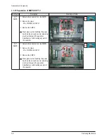
Page 21: ...ear gloves when handling the power board as there may be some remaining electrical charge in the capacitor Specifically avoid touching any part of the capacitor 50 SMPS Detach all connectors from the SMPS Remove 8 screws PH WWP M3 L8 NI PLT Remove the SMPS Wear gloves when handling the power board as there may be some remaining electrical charge in the capacitor Specifically avoid touching any par...

Page 22: ...BOARD Part Name Description Description Photo 42 Logic Board Detach all connectors from the Logic Main Board Remove 4 screws WSP PH M3 L8 NI PLT Remove the Logic Main Board 50 Logic Board Detach all connectors from the Logic Main Board Remove 4 screws WSP PH M3 L8 NI PLT Remove the Logic Main Board ...

Page 23: ...n Description Photo Flat Cable Detach all Connectors from the X Main Board To separate the Flat Cable of the X Board press the upper and the lower sides of the connector 42 X Main Board Remove 4 screws PH WWP M3 L8 NI PLT Remove the X Main Board 50 X Main Board Remove 4 screws PH WWP M3 L8 NI PLT Remove the X Main Board ...

Page 24: ...DULE P Y MAIN BOARD Part Name Description Description Photo Flat Cable Detach the 6 scan board connectors from the panel by pulling the holder from both the top and bottom ends 42 Y Scan Board Remove 3 screws PH WWP M3 L8 NI PLT 50 Y Scan Board Remove 5 screws PH WWP M3 L8 NI PLT ...

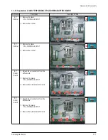
Page 25: ...ctronics Part Name Description Description Photo 42 Y Main Board Remove 4 screws PH WWP M3 L8 NI PLT Detach all connectors from the Y Main Board 50 Y Main Board Remove 4 screws PH WWP M3 L8 NI PLT Detach all connectors from the Y Main Board ...

Page 26: ...s PH WWP M3 L8 NI PLT Remove the still bar 50 Still Bar Remove 4 screws PH WWP M3 L8 NI PLT Remove the still bar 42 Buffer Board Detach the all connectors from the buffer board Remove 12 screws PH WWP M3 L8 NI PLT Remove the E Board and F Board 50 Buffer Board Detach the all connectors from the buffer board Remove 14 screws PH WWP M3 L8 NI PLT Remove the E Board and F Board ...

Page 27: ...e 2 screws BH B M4 L3 ZPC BLK Remove the Function Board Disassembly Reassembly 3 12 Samsung Electronics 3 1 15 Separation of ASSY PANEL BRACKETS Part Name Description Description Photo Panel Brackets Remove 3 screws BH B M4 L3 ZPC BLK Remove 4 screws BH S M4 L10 ZPC BLK Remove the Side Panel Brackets ...

Page 28: ... or damaged cable Check to see if there is a disconnected or loose cable connection Check to see if the cables are connected according to the connection diagram 2 Check the power input to the Main Board 3 Check the voltage in and out between the SMPS Main Board between the SMPS X Y Main Board and between the Logic Boards 4 Troubleshooting 4 1 Troubleshooting ...

Page 29: ...mproperly connected or the Main Board or SMPS is not functioning In this case check the following Check the internal cable connection status inside the unit Check the fuses of each part Check the output voltage of SMPS Replace the Main Board Troubleshooting Procedures Is the AC IN socket connector and the SMPS CN800 connected Insert the AC in connector and the SMPS CN800 connector Is the Fuse F801...

Page 30: ... defective assemblies by connecting the cables one by one Troubleshooting Procedures Caution When separating and connecting the cables such as CN810 CN809 CN808 CN807 of the Main SMPS CN4701 of the X Main Board and CN5707 of the Y Main Board a spark may be generated by the electric charge of the high capacity capacitor Therefore wait some time after disconnecting the power cord from the unit Does ...

Page 31: ...eparating and connecting the cables such as CN810 CN809 CN808 CN807 of the Main SMPS CN4701 of the X Main Board and CN5707 of the Y Main Board a spark may be generated by the electric charge of the high capacity capacitor Therefore wait some time after disconnecting the power cord from the unit CN810 CN809 CN808 CN807 Are the Vs and Va voltages normal after removing all cables from the SMPS CN810 ...

Page 32: ... the Main Board is not functioning Speaker defect Troubleshooting Procedures Is the cable connection between the Main Board and the speaker properly connected Connect the cable properly or replace the cable if necessary Is the output voltage of SMPS normal CN801 13 Replace the SMPS Replace the Main Board Is the speaker output terminal of the Main Board normal Replace the Speaker Yes No No No Yes Y...

Page 33: ...is OK Major Checklist Check the antenna connection settings Air NTSC ATSC Cable NTSC Check the CVBS cable connection Check the power input of the Main board Troubleshooting Procedures Is the antenna connection setting properly configured Configure properly Replace the SMPS Check CN1101 pin2 for 5V Replace the Main Board No No Yes Yes ...

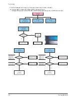
Page 34: ...mal Check the U101 D108 PFC Normal Abnormal Check the U201 Q203 Q204 VA Multi Check the U501 Abnormal Abnormal Check the U601 Normal VS Normal Abnormal Check the Q401 Q402 Check the Other board Image Board or Driver Board or Cable Power ON SMPS Troubleshooting ...

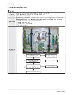
Page 35: ...l Image not open or short is no screen Y MAIN X MAIN Logic Main Sustain Open Some horizontal lines don t exist on screen Scan Buffer FPC of X Y Sustain Short Some horizontal lines appear to be linked on screen Scan Buffer FPC of X Y Address Open Some vertical lines don t exist on screen Logic Main Logic Buffer TCP Address Short Some vertical lines appear to be linked on screen Logic Main Logic Buf...

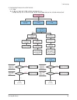
Page 36: ...ates a PSU output error Check the FUSE Check the input voltage YES NO YES NO Y MAIN Check several points FUSE FET DIODE Y MAIN Normal State Replace the Board Replace the Board OK OPEN SHORT OK F5001 for VDD F5002 for Vs F5004 for VCC F5005 for OUT_L Q5009 Q5021 D5005 D5007 D5008 X MAIN Check several points FUSE FET DIODE X MAIN Normal State Replace the Board Replace the Board OK OPEN SHORT OK F400...

Page 37: ...oard Replace the Board OK OPEN SHORT OK F5001 for VDD F5002 for Vs F5004 for VCC F5005 for OUT_L Q5009 Q5021 X MAIN Check several points FUSE FET X MAIN Normal State Replace the Board Replace the Board OK OPEN SHORT OK F4001 for VCC F4002 for Vs F4004 for VDD F4005 for Ve Q4002 Q4003 Q4011 Q4016 Abnormal Display Abnormal Image is on Screen except abnormality in Sustain or Address Abnormal Display ...

Page 38: ...echeck the status Done Defect is from Y buffer Replace the Panel There is a defect on the FPC OK NG Sustain Short some horizontal lines appear to be linked on Video Y FPC Sustain Short Discharging in unwanted Scan line After Changing Y buffer recheck the status Done Defect is from Y buffer OK NG Replace the Panel There is a defect on the FPC ...

Page 39: ...nternal mode screen is normal Reload the data onto the MICOM and recheck it Check if there is an open or short circuit on the Buffer Board and the Logic Main address data output section Check the FFC connection status Check the detailed waveform and control the signal waveform OK NG OK NG Check if a specific TCP Block screen is displayed abnormally OK NG OK Replace Logic Main Address Buffer E or F...

Page 40: ... upper lower buffers E F COF defect burnt Replace the module A green screen appears when the TV is turned on The Scale is not reseting Replace the Main board The OSD box appears but there is no text Incorrect program version Check the version of each program Replace the Main board A blank upper or lower block appears on the screen Upper Lower Y Buffer defect Replace the corresponding upper lower b...

Page 41: ...icture does not appear Replace the Main board A vertical green line appears on the screen The SMPS voltage is incorrect Adjust the SMPS voltage according to the voltage printed on the module label Dim screen blurred in red X Main board defect Replace the X Main board A blank screen appears Replace the Y Main board ...

Page 42: ...ER Row Bar screen is blank 6 ASSY PDP MODULE P ADDRESS E BUFFER Corresponding Buffer Board block screen is blank 7 ASSY PDP MODULE P ADDRESS F BUFFER Corresponding Buffer Board block screen is blank 8 ASSY PCB MISC MAIN No Power Abnormal screen for each input source PIP screen trouble Sound trouble 9 ASSY BOARD P FUNCTION The side function key does not work properly 10 ASSY BOARD P POWER IR The re...

Page 43: ...eplacement of Board If adjustment equipment is available PDP Option of Factory Mode set the Factory Data Type item as the suitable value of relevant model Adjust Calibration of Factory Mode for each mode Adjust White Balance of Factory Mode If adjustment equipment is not available Write down the value of HDMI White Balance of Factory Mode before replacing Board PDP Option of Factory Mode set the F...

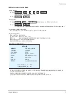
Page 44: ...ode Using the Numeric 0 9 keys you can select a channel Using the SOURCE key you can switch AV modes 5 Initial SERVICE MODE DISPLAY State The version of the firmware displayed at the bottom of the screen may differ and the firmware is subject to change for the improvement of product functions If you have adjusted the settings in Service Mode you have to reset the product If you exit Service Mode w...

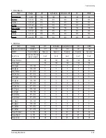
Page 45: ... On On On On On RS 232 JACK AutoWM AutoWM AutoWM AutoWM AutoWM Gamma 0 9 0 9 0 9 0 9 0 9 HSCB STD STD STD STD STD LVDS_TX_Fmt 0 0 0 0 0 LVDS_TX_Bit 12Bit 12Bit 12Bit 12Bit 12Bit Panel Display Time 0Hr 0Hr 0Hr 0Hr 0Hr Mute Time RF 2 2 2 2 2 CH Memory SAMEX SAMEX SAMEX SAMEX SAMEX shop mode Off Off Off Off Off Downloadable RRT On On On On On PC Mode ident Auto Auto Auto Auto Auto IRE Off Off Off Off...

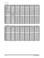
Page 46: ... Dynamic Dynamic Dynamic Dynamic Color Tone Coo2 Cool1 Normal Warm1 Warm2 Cool1 Cool1 Cool1 Cool1 Cool1 Msub Contrast 128 128 128 128 128 Msub Bright 128 128 128 128 128 W2_Rgain 127 128 0 0 0 0 0 W2_Bgain 127 128 0 0 0 0 0 W2_Roffset 511 512 0 0 0 0 0 W2_Boffset 511 512 0 0 0 0 0 W1_Rgain 127 128 0 0 0 0 0 W1_Bgain 127 128 0 0 0 0 0 W1_Roffset 511 512 0 0 0 0 0 W1_Boffset 511 512 0 0 0 0 0 Nor_Rg...

Page 47: ...8 8 8 8 Roffset 68 68 67 110 67 Goffset 68 68 67 110 67 Boffset 68 68 67 110 67 RGain 294 294 274 265 274 GGain 294 294 274 265 274 BGain 294 294 274 265 274 Item Range RF AV S video Component HD PC HDMI H2gain 10 10 10 10 10 H4gain 10 16 16 10 16 V2gain 10 10 10 10 10 V4gain 10 16 16 10 16 Sr2gain 0 0 0 0 0 Sr4gain 0 0 0 0 0 Sl2gain 0 0 0 0 0 Sl4gain 0 0 0 0 0 Peakth1 4 4 4 4 4 Peakth2 47 47 47 4...

Page 48: ...dB3_NoiseAmount 14 14 0 0 0 dB3_Peaking_th1 128 128 0 0 0 dB3_Vpeaking_th1 80 80 0 0 0 Item Range RF AV S video Component HD PC HDMI U Delay 0 0 0 0 0 V Delay 0 0 0 0 0 UV Delay Item Range RF AV S video Component HD PC HDMI TCD3_Contrast 114 114 126 126 126 TCD3_Bright 45 45 40 40 40 TCD3_YC_Delay 0 0 0 0 0 ANALOG_Y_Offset 66 66 67 20 66 ANALOG_PB_Offset 128 128 128 23 128 ANALOG_PR_Offset 128 128...

Page 49: ..._PC_Low 0x4 0x4 0x4 0x4 0x4 1st_PC_High 0xEB 1xEB 1xEB 0xEB 0xEB 1st_PC_Delta 0x4 0x4 0x4 0x4 0x4 None None None 2nd_AV_Low 0x1 0x1 0x1 0x1 0x1 2nd_AV_High 0xEB 1xEB 1xEB 0xEB 0xEB 2nd_AV_Delta 0x8 0x8 0x8 0x8 0x8 2nd_COMP_Low 0x1 0x1 0x1 0x1 0x1 2nd_COMP_High 0xEB 1xEB 1xEB 0xEB 0xEB 2nd_COMP_Delta 0x8 0x8 0x8 0x8 0x8 2nd_PC_Low 0x1 0x1 0x1 0x1 0x1 2nd_PC_High 0xEB 1xEB 1xEB 0xEB 0xEB 2nd_PC_Delt...

Page 50: ... 120 120 Skin Enable 1 1 1 1 1 Skin Tu 130 130 130 128 134 Skin Tv 130 130 130 128 134 Sub Color 128 128 140 130 140 M Skin Tu 100 100 100 100 100 M Skin Tv 100 100 100 100 100 M Au Sub color 128 128 128 128 128 MW_Skin Tu 100 100 100 100 100 MW_Skin Tv 100 100 100 100 100 M Wi Sub color 128 128 128 128 128 7 MSP44XX Item Range RF AV S video Component HD PC HDMI FM_Precale 31 31 31 31 31 Melody Vo...

Page 51: ...xD 0xD 0xD 0xD 0xD VSB 0xC 0xC 0xC 0xC 0xC VSB 0x12 0x12 0x12 0x12 0x12 VSB 0x10 0x10 0x10 0x10 0x10 VSB 0x11 0x11 0x11 0x11 0x11 VSB 0x10 0x10 0x10 0x10 0x10 VSB_EQ_CTRL1 0x30E 0x30E 0x30E 0x30E 0x30E VSB_EQ_CTRL2 0x104 0x104 0x104 0x104 0x104 VSB_EQ_INIT_STEP 0x3161 0x3161 0x3161 0x3161 0x3161 VSB_EQ_STEP 0x6111 0x6111 0x6111 0x6111 0x6111 VSB_PTL_STEP 0x522 0x522 0x522 0x522 0x522 VSB_PTL_ALPHA...

Page 52: ...0 0 Model Select CALLQ90 CALLQ90 CALLQ90 CALLQ90 CALLQ90 Panel Select W2A W2A W2A W2A W2A Panel Type No Info No Info No Info No Info No Info Panel Version W2 W2 W2 W2 W2 Logic SW Version 61128 61128 61128 61128 61128 Factory Update Off Off Off Off Off Factory Data Type NONE NONE NONE NONE NONE CDC_SW OFF OFF OFF OFF OFF CDC_STRENG_TH 0 0 0 0 0 BRE_SE OFF OFF OFF OFF OFF PANEL TEMP 0 0 0 0 0 15 RES...

Page 53: ...n 24 Chess Pattern 4 Use Equipment CA210 Master MSPG925 Generator Use other equipment only after comparing the result with that of the Master equipment Chess Pattern Input mode Calibration Pattern CVBS IN Model_ 1 Perform in NTSC B W Pattern 24 Lattice Component IN Model_ 6 Perform in 720p B W Pattern 24 Lattice PC Analog IN Model_ 21 Perform in VESA XGA 1024x768 B W Pattern 24 Lattice HDMI IN Per...

Page 54: ... is complete it returns to the high level menu 8 You can see the change of the Comp Calibration status from Failure to Success Method of Color Calibration PC 1 Apply the VESA XGA Lattice N0 21 pattern signal to the PC IN port 2 Press the Source key to switch to PC mode 3 Enter Service mode 4 Select the Calibration menu 5 Select the PC Calibration menu 6 In PC Calibration Off status press the key t...

Page 55: ...ut to HDMI mode Enter the White Balance menu of service mode Contact CA 210 sensor to glass filter Adjust the low light Adjust Sub Bright LBE to set the Y value Adjust R Offset x and B Offset y to the color coordinates Do not adjust G Offset data Adjust the high light Adjust Sub Contrast LBE to set the Y value Adjust R Gain x and B Gain y to the color coordinates Do not adjust the G gain data SAMS...

Page 56: ...L1 10 500 0 0 L L 2780 5 2850 5 1 0fL0 0 3fL 10 500 0 0 COMP 720P H L 2780 3 2850 3 23fL 20fL1 10 500 0 0 L L 2780 5 2850 5 1 3fL0 0 2fL 10 500 0 0 HDMI 720P H L 2780 3 2850 3 23fL 20fL1 10 500 0 0 L L 2780 5 2850 5 1 2fL0 0 1fL 10 500 0 0 PC XGA 1024 768 H L 2790 5 2940 5 21fL 20fL1 L L 2870 5 2970 5 0 8fL0 0 2fL ...

Page 57: ...items listed after changing each Replaced assembly items Check Items ASSY PCB MISC MAIN 1 Auto Program 2 White Balance Adjust SMPS PDP TV Vs Va voltage check and adjust ASSY PDP MODULE P LOGIC MAIN Not to be adjusted ASSY PDP MODULE P X MAIN ASSY PDP MODULE P Y MAIN ASSY PDP MODULE P Y MAIN SCAN BUFFER ASSY PDP MODULE P Y MAIN SCAN BUFFER ASSY PDP MODULE P ADDRESS E BUFFER ASSY PDP MODULE P ADDRES...

Page 58: ...Va Adjustment Va Test point Vs Test point Value Board Adjustment Vs 210 SMPS Va 63 Vset Ve 94 Vscan 190 Voltage Adjustment 1 After replacing the SMPS or PDP panel you must adjust the voltage referring to the voltage label printed on the panel If you do not adjust the voltage an abnormal discharge symptom may appear ...

Page 59: ...32 Samsung Electronics Y RR and Y FR controls 60usec 80usec Test Point Rising ramp variable resistor Falling ramp variable resistor Set the main reset rising 60usec falling 80usec by change the value of variable resistor ...

Page 60: ...ade in Menu SETUP Select the SW Upgrade from the menu Select USB from the menu The banner OSD Scaning for USB is displayed 3 The banner OSD Upgrade version to version is displayed Select Yes 4 The banner OSD Upgrade version to version is displayed It takes about 30 sec Warning Don t remove USB flash driver during upgrade 5 The banner OSD Upgrade is completed is displayed when the upgrade is comple...

Page 61: ...Menu Select the Setup menu in the Menu screen Place the cursor over the On of Function Help and press the Info key on the remote control The version of the program is displayed at the bottom of the Menu screen 2 How to check Program Version on factory mode MAIN PROGRAM VERSION MICOM VERSION MAIN PROGRAM VERSION MICOM VERSION ...

Page 62: ...4 35 Samsung Electronics MEMO ...

Page 63: ...ded View Part List 5 Exploded View Part List 5 1 HPT4254X XAA Exploded View T0074 T0268 T0175 T0456 M0146 M0105 M0149 T0044 M0412 T0079 T0915 M0013 M0013 T0920 M0111 T0003 M0146 M0150 M0112 T0023 T0023 CIS7 T0056 M0105 M0145 M0020 ...

Page 64: ... ASSY BRACKET P FILTER TOP 42Q9 AL6063 T1 1 S N A M0150 BN96 04686A ASSY BRACKET P FILTER BOTTOM 42Q9 AL6063 1 S N A M0150 BN96 04691B ASSY BRACKET P SUPPORT FILTER 42Q9 Al 60 1 S N A M0412 BN96 04903A ASSY BRACKET P PCB Q9 SECC 0 8 1 S N A T0003 BN96 04712B ASSY COVER P FRONT 42C9 ABS HB BK23 STEA 1 S A T0023 BN96 04707A ASSY COVER P KNOB POWER C9 Q9 ABS HB 1 S N A T0023 BN64 00567A KNOB POWER 42...

Page 65: ...ics 5 3 Exploded View Part List 5 2 HPT5054X XAA Exploded View T0074 T0268 T0003 M0146 M0150 M0112 T0023 T0023 CIS7 T0056 M0105 M0145 T0175 T0456 M0146 M0105 M0149 T0044 M0013 T0920 M0111 T0915 T0079 M0412 M0013 M0020 ...

Page 66: ...A ASSY BRACKET P FILTER TOP 50Q9 AL6063 T1 1 S N A M0150 BN96 04692A ASSY BRACKET P SUPPORT FILTER 50Q9 AL606 1 S N A M0150 BN96 04689A ASSY BRACKET P FILTER BOTTOM 50Q9 AL6063 1 S N A M0412 BN96 04903A ASSY BRACKET P PCB Q9 SECC 0 8 1 S N A T0003 BN96 04713B ASSY COVER P FRONT 50C9 ABS HB BK23 STEA 1 S A T0023 BN96 04707A ASSY COVER P KNOB POWER C9 Q9 ABS HB 1 S N A T0023 BN64 00567A KNOB POWER 4...

Page 67: ...1 T0074 BN59 00599A REMOCON Bordeaux plus TM87C SAMSUNG28P E 1 T0079 BN94 01226A ASSY PCB MISC MAIN HPT4254X C9 F34B LIL 1 T0175 BN96 04704A ASSY SPEAKER P 8ohm C9 10W 4P connector 1 T0764 BN44 00159A SMPS PDP TV PS42P7H DYREL AC DC 370W AC1 1 T1910 BN96 04593A ASSY PDP MODULE P X MAIN 42HD W2 PL42AX0 1 T1911 BN96 04594A ASSY PDP MODULE P Y MAIN 42HD W2 PL42AX0 1 T1914 BN96 04597A ASSY PDP MODULE ...

Page 68: ...rdeaux plus TM87C SAMSUNG28P E 1 T0079 BN94 01230A ASSY PCB MISC MAIN HPT5054X C9 F34B LIL 1 T0175 BN96 04704A ASSY SPEAKER P 8ohm C9 10W 4P connector 1 T0764 BN44 00160A SMPS PDP TV PS50P7H DYREL AC DC 460W AC1 1 T1910 BN96 04573A ASSY PDP MODULE P X MAIN 50HD W2 PL50HW0 1 T1911 BN96 04574A ASSY PDP MODULE P Y MAIN 50HD W2 PL50HW0 1 T1914 BN96 04578A ASSY PDP MODULE P ADDRESS E_BU 50HD W2 P 1 T19...

Page 69: ...Samsung Electronics 5 7 MEMO ...

Page 70: ...N809 CN808 CN810 CN4701 CN4002 CN4001 CN4004 CN2004 CN2600 CN2610 CN2510 CN1 CN3 CN800 LOGIC BOARD SMPS X DRIVE Y DRIVE Y MAIN SCAN AC INLET F BUFFER FUNCTION POWER SW CN101 SIDE AV CN2609 CN2000 CN2001 CN2006 SPEAKER CN801 CN2002 CN1605 CN1606 CN1203 MAIN BOARD 8 9 10 11 CN2028 3 4 5 6 7 CN1101 CN2202 CN1404_SIDE 2 CN2003 E BUFFER CN2500 CN2509 1 42 Overall Wiring ...

Page 71: ...N2510 CN1 CN3 CN800 LOGIC BOARD SMPS X DRIVE Y DRIVE Y MAIN SCAN HIGH F BUFFER FUNCTION POWER SW CN101 SIDE AV Y MAIN SCAN LOW CN2609 CN2003 CN2000 CN2001 CN2006 CN2005 SPEAKER CN801 CN2002 MAIN BOARD CN2500 CN2509 E BUFFER 4 5 6 7 3 8 10 11 9 CN1101 CN2202 CN1605 CN1606 CN1203 CN1404_SIDE 2 1 AC INLET 50 Overall Wiring Wiring Diagram 6 2 Samsung Electronics ...

Page 72: ... Exploded View Part List Use LVDS 31P 30P POWER 24P Flat Cable Code 42 BN39 00826A 50 BN39 00859A 42 BN39 00802K 50 BN39 00802C 42 BN96 05164A 50 BN96 05176A Photo Use Y Drive X Drive Address Code Photo Use Logic Front SPEAKER Code Photo Use FUNCTION AC_INPUT Code 42 2901 001378 50 2901 001340 Photo ...

Page 73: ...ND_STBY 16 5V 5 GND_18V AMP 17 GND_12V 6 GND_18V AMP 18 GND_12V 7 18V AMP 19 12V 8 18V AMP 20 GND_12V 9 GND_5V 21 12V 10 GND_5V 22 12V 11 GND_5V 23 N C FAN_ON 12 GND_5V 24 N C FAN_DET CN1404 MAIN B D CN101 SIDE AV Pin No Signal Pin No Signal Pin No Signal Pin No Signal 1 GND 12 TXC 23 NC 34 VIDEO_SR_IN 2 TX2 13 GND 24 NC 35 VIDEO_SL_IN 3 TX2 14 MICOM_CEC 25 GND 36 HP_IDENT 4 GND 15 GND 26 SVHS_IDE...

Page 74: ...3 MAIN B D SPEAKER Pin No Signal 1 R _OUT 2 R _OUT 3 L _OUT 4 L _OUT CN1605 MAIN B D FUNCTION Pin No Signal 1 KEY_INPUT1 2 KEY_INPUT2 3 GND CN800 SMPS AC INLET Pin No Signal 1 AC Neutral 2 N C 3 AC Live CN807 SMPS CN2000 LOGIC B D Pin No Signal 1 STBY 2 VS_ON 3 N C 4 PS_ON 5 RTN 6 5 3V 7 RTN 8 RTN 9 5 3V 10 5 3V CN1606 MAIN B D POWER IR Pin No Signal 1 IR 2 GND 3 A5V_1 4 LED_STB 5 BUZZER 6 KEY_INP...

Page 75: ... CN807 SMPS and Logic Board Connect CN801 CN801 SMPS and Main Board Connect CN800 CN800 SMPS and AC Inlet Connect CN4701 CN4701 SMPS and X Drive Connect CN4004 CN4004 Logic Board and X Drive Connect CN4002 CN4002 Module and X Drive Connect CN4001 CN4001 Module and X Drive Connect CN4000 Module and X Drive Connect CN2000 CN2000 SMPS and Logic Board Connect CN2001 CN2001 Main Board and Logic Board C...

Page 76: ... Loc No Description CN1606 CN1606 Power SW Assy and Main Board Connect CN1203 CN1203 Speaker and Main Board Connect CN101 CN101 Side AV Assy and Main Board Connect CN1 CN1 Function Assy and Main Board Connect CN3 CN3 Power SW Assy and Main Board Connect ...

Page 77: ...6 8 Samsung Electronics MEMO ...

Page 78: ...d decodes the video signal encoded by the Video Board outputs the ADDRESS data signal for each pattern and generates X and Y drive signals The Address Buffer Board buffers and transfers the ADDRESS data output signal using TCP IC LVDS with built in video signal processing W L error diffusion APC FCR etc applied and 1 ASIC chip Outputs the address Drive IC control and data signals to the Buffer Boa...

Page 79: ...7 2 Samsung Electronics MEMO ...

Page 80: ...L A V L P U S 1 2 1 P T 1 7 4 1 C F u 0 0 1 V 6 1 5 1 1 C I A D 7 1 1 1 P A J D A 1 2 T U O V N I V 3 V 5 B E K A L _ V 5 2 V 5 2 F u 0 0 1 8 8 1 C 8 6 1 C 3 1 1 D B 2 9 1 C F n 0 0 1 V 6 1 V 3 6 F u 0 2 1 1 L 5 1 1 P T 1 3 0 1 L 1 2 3 1 1 P T L A V L P U S F n 0 0 1 8 1 1 R m h o K 6 3 W 0 1 1 8 7 1 C F p 0 8 1 3 7 1 C L 2 6 1 C F n 0 0 1 6 1 1 D B 9 7 1 C E R O C _ V 2 1 0 7 1 C F n 0 0 1 V 5 2 ...

Page 81: ...0 1 1 S P K 1 0 2 W S 1 2 3 5 1 2 R m h o K 1 V 5 A D 4 2 2 D F S W 8 4 1 4 N 1 m h o 0 1 8 2 2 R 1 0 2 C V 6 1 F u 0 1 TP207 1 10Kohm R210 V 5 A m h o K 2 2 6 5 2 R F n 0 0 1 3 0 2 C V 6 1 F u 1 10Kohm R247 R281L 1 5Kohm 9 0 2 C 0 1 2 Q Y 3 2 6 1 C S K E B C 6 1 2 P T 1 8 1 2 D 1 1 E T B 6 5 Z L R 10Kohm R208 10Kohm R267 R213 10Kohm V 6 1 D 4 2 2 C F u 0 1 1 10Kohm R203 1 2 3 F E R X 4 2 2 P T m ...

Page 82: ... 5 T Z B F E R X F E R X F E R X 1 0 3 D 8 Q Y B D N A T S 0 8 9 I2S_DEL_OUT F E R X 1 10W 2 3 3 R 470Kohm 2 7 3 7 C N C N 4 7 5 7 C N T U O _ F I D P S 6 7 1 _ O I R T C D 7 7 0 _ O I R T C D 8 7 9 7 L E S _ R D A I2S_DEL_IN 2 N I _ A N A N E T S E T 6 6 7 6 N I _ L A T X T U O _ L A T X 8 6 9 6 P T 7 I2S_DA_IN1 T U O _ L C _ D U A 0 7 1 7 C N C N 58 59 AVSS I2S_DA_OUT 6 AVSS 60 1 6 P U S V A 2 6...

Page 83: ...4 C V 5 2 F n 0 0 1 m h o K 7 4 3 1 4 R W 0 1 1 V 0 5 F n 0 0 1 m h o 7 4 7 1 4 R 3 2 4 R m h o K 3 3 1 0 4 D B D N G S L L P _ D D V D F E R X F n 0 0 1 V 0 5 8 0 4 C V 0 5 F n 1 0 1 4 C m h o 7 4 D408 1N4148WS F 4 2 4 R 8 2 4 C D N G S 6 0 4 D B V 0 5 F n 1 V 0 5 F n 1 F u 1 V 0 1 SGND 7 2 4 C F u 0 1 1 0 4 C V 6 1 9 1 4 C 1 4 0 4 C V 0 5 F n 1 F n 1 V 0 5 5 2 4 C 5 0 4 P T 7 0 4 P T 1 D401 1N41...

Page 84: ...1 F u 2 2 2 1 5 C 6 1 5 P T 1 m h o K 0 0 1 6 0 5 R E B C 3 Y 3 2 6 1 C S K 2 0 5 Q 2 0 5 C I A D 7 1 1 1 P A J D A 1 2 T U O V N I V 1 7 0 5 P T 1 1 5 0 5 P T 1 6 0 5 P T 6 7 8 3 0 5 P T m h o 3 3 2 0 5 A R W 6 1 1 1 2 3 4 5 5 0 5 R W 0 1 1 m h o K 0 2 2 C m h o K 0 2 2 W 0 1 1 7 0 5 R 1 0 5 Q Q K 2 1 4 2 C S 2 E B W 0 1 1 4 0 5 R m h o K 0 0 1 1 1 5 C F n 0 0 1 V 6 1 2 0 5 L H u 0 8 6 2 0 5 P T ...

Page 85: ...m h o 0 1 CDS3C30GTH D603 1 2 6 1 6 P T 1 F n 0 0 1 1 3 6 C H 3 7 6 R m h o 0 H 4 7 6 R F u 0 1 m h o 0 4 0 6 L 9 2 6 C 1 1 0 6 R m h o 0 0 1 H 9 4 6 P T 1 9 0 6 P T 1 H 8 4 6 P T 1 D601 CDS3C30GTH 1 2 6 0 6 P T D628 CDS3C30GTH 1 2 9 0 6 L m h o 0 7 4 4 1 6 R 2 0 6 L F n 0 0 1 8 2 6 C 6 2 6 P T 1 9 4 6 R m h o 0 0 1 F n 0 0 1 CDS3C30GTH 1 2 2 3 6 C H T G 0 3 C 3 S D C 1 1 6 D 1 2 D637 8 0 6 P T 1 ...

Page 86: ... 8 1 0 7 P T m h o 0 B 3 0 7 A R W 6 1 1 7 1 7 P T 1 S 8 1 7 R m h o 0 2 1 7 P T 1 5 0 7 D B T J 0 0 6 8 0 6 1 M 1 H H 1 2 S 0 2 7 R m h o 0 D741B CDS3C30GTH B 2 0 7 L m h o 7 4 B 2 5 7 R 6 4 7 R m h o 0 1 B 4 3 7 R m h o 0 m h o 7 4 B 2 3 7 R F u 0 1 V 6 1 B 0 1 7 P T 1 1 B 0 1 7 C D703B CDS3C30GTH 1 2 5 2 7 P T 3 2 7 P T 1 0 2 7 P T 1 1 2 3 H T G 0 3 C 3 S D C B 4 0 7 D 1 2 MMBD4148SE D720B H T ...

Page 87: ...4 8 C V 5 2 1 m h o 0 1 5 6 8 R m h o K 0 1 7 4 8 R 3 0 8 P T 4 0 8 D 1 2 3 9 1 8 R 1 2 8 P T 1 7 3 8 C F n 0 0 1 m h o 0 1 V 6 1 7 0 8 R 9 8 8 R m h o K 7 4 2 0 8 L H u 0 1 m h o K 1 6 2 8 R m h o 5 7 3 4 8 R m h o 0 0 1 m h o 0 D 3 8 8 R 3 3 8 P T 1 4 3 8 P T 1 3 9 8 R m h o K 0 1 5 0 8 P T 1 2 5 8 R V 0 5 F p 9 3 9 4 8 C m h o 7 4 L 2 0 0 7 N 2 1 0 8 Q V 5 2 8 2 8 C F n 0 0 1 m h o 0 1 1 6 8 R ...

Page 88: ..._ V 3 3 B 5 0 0 1 D B F n 0 0 1 V 6 1 V 6 1 F u 0 1 5 1 0 1 C 2 5 0 1 C V 0 5 3 4 0 1 C F u 0 1 V 6 1 F n 7 2 3 2 0 1 C 3 1 0 1 D B W 0 1 1 m h o K 5 1 5 0 0 1 R F n 0 0 1 8 0 0 1 C m h o K 0 1 3 3 0 1 C F n 0 0 1 4 0 0 1 R F n 0 0 1 2 0 0 1 D B 7 5 0 1 C F n 0 0 1 8 2 0 1 C F n 0 0 1 1 2 0 1 C F n 0 0 1 7 4 0 1 C 2 4 0 1 C F u 0 1 F n 0 0 1 0 5 0 1 C V 6 1 V 6 1 F u 0 1 9 0 0 1 D B 9 0 0 1 C 6 0 ...

Page 89: ... 3 D M 9 3 1 0 M Q D 4 1 1 _ N F E R V 0 4 1 M D D V 127 TA1P 128 TA1M 9 2 1 O S S V _ S D V L 3 1 1 _ P F E R V 0 3 1 O D D V _ S D V L 1 3 1 A D D V _ S D V L 2 3 1 A S S V _ S D V L 3 3 1 D S S V _ S D V L 2 1 1 B F 120 TD1M TCLK1P 121 122 TCLK1M 123 TC1P 124 TC1M 125 TB1P 126 TB1M 112 V5SF 113 LVDS_VSSP 114 LVDS_VDDP 115 LVDS_VSSO 116 LVDS_VDDO 117 TE1P 118 TE1M 119 TD1P 105 SDA 106 SCL VDDC 1...

Page 90: ...Q D D V D12 DQ24 2 D Q D D V D3 VDD 4 D S S V D5 VSSQ 6 D S S V C3 VSSQ C4 VSSQ C5 VSSQ C6 VDD C7 VDD C8 VSSQ C9 VSSQ 1 D 7 Q D 7 B Q D D V B8 DQ30 9 B Q D D V 1 C 6 Q D C10 VSSQ C11 DQ26 C12 DQ25 2 C 5 Q D B10 NC 1 1 B Q D D V DQ27 B12 B2 VDDQ B3 NC B4 VDDQ 5 B 1 Q D 6 B Q D D V A3 VSSQ 4 A 3 Q D 5 A 2 Q D 6 A 0 Q D A7 DQ31 A8 DQ29 A9 DQ28 1 B 4 Q D G M 5 I B 0 2 3 9 A 6 M E 1 0 2 1 C I A1 DQS0 A...

Page 91: ... 1 3 1 4 1 1 F E R X 10nF C947 L A V L P U S 7 1 9 P T m h o 0 8 0 9 R C943 100nF C948 10nF F E R X m h o 0 F E R X m h o 0 0 1 7 1 9 R G N I R _ 3 R _ R W P 8 N G N I R _ 3 R _ R W P G N I R _ R _ D N G 9 N 2 _ A 3 3 D D V A 3 P 3 R 2 _ A 3 3 S S V A 1 1 9 R 1 1 N 2 1 N G N I R _ 1 R _ R W P 3 1 N G N I R _ R _ D N G 4 1 N 1 _ A I 2 1 S S V A 2 _ P 3 3 S S V A 3 N G N I R _ 1 R _ R W P 4 N G N I ...

Page 92: ... h o 0 m h o 0 0 1 6 3 3 1 R 3 2 0 4 R m h o 0 R1376 R4010 4 7Kohm V 0 5 4 7Kohm V 6 1 F u 0 0 1 1 1 3 1 C F n 1 8 0 3 1 C C C V _ C D D 7 0 3 1 P T 1 6 0 3 1 Q Y 3 2 6 1 C S K E B C D 3 5 3 1 R m h o 0 1 _ V 3 3 B 4 7Kohm R1374 m h o 0 4 3 3 1 R m h o 3 3 6 6 3 1 R V 6 1 F u 2 2 2 2 3 1 C R1381 4 7Kohm m h o 0 0 1 9 4 3 1 R 0 6 3 1 R m h o 3 3 Y 3 2 6 1 C S K 5 0 3 1 Q E B C m h o 3 3 2 3 3 1 R V...

Page 93: ...ohm R1436 4 0 4 1 A R m h o 0 0 1 4 0 4 1 R 4 5 4 1 R m h o 0 0 1 m h o 0 0 1 3 5 4 1 R F E R X F E R X F E R X F E R X F E R X F E R X F E R X F E R X 6 2 I 6 O 7 8 3 I 9 7 O F E R X F E R X F E R X F E R X 4 I 7 1 8 1 0 O 9 1 2 E O 0 I 2 C C V 0 2 4 O 3 4 1 I 5 O 5 1 1 E O D N G 0 1 1 1 7 I 3 O 2 1 6 I 3 1 2 O 4 1 5 I 5 1 6 1 1 O 2 0 4 1 C I 2 R T D 4 4 2 C H V 4 7 C M R1418 4 7Kohm m h o 0 0 1 ...

Page 94: ... 2 E 5 2 F 2 M Q D M B 6 2 F 2 S Q D M B 5 2 G 3 2 Q D M B 2 2 Q D M B 6 2 G 1 2 Q D M B 4 2 H 5 2 H 6 2 E A 3 Q D M B 5 2 F A 0 Q D M B 1 Q D M B 6 2 F A 5 2 B 9 2 Q D M B 8 2 Q D M B 6 2 B 7 2 Q D M B 5 2 C 6 2 C 6 2 Q D M B 5 2 Q D M B 5 2 D 6 2 D 6 2 A A 5 2 B A 0 S Q D M B 6 2 B A 0 M Q D M B 6 Q D M B 5 2 C A 6 2 C A 7 Q D M B 5 2 D A 4 Q D M B 5 Q D M B 6 2 D A 2 Q D M B 5 2 E A 2 1 0 3 1 C...

Page 95: ...1 R 0 1 A 9 A 8 8 A 9 m h o K 7 4 8 0 6 1 R 6 Q D 4 1 Q D 4 4 5 4 7 Q D 5 1 Q D 6 4 E O 7 4 8 4 S S V 2 1 A 5 1 1 A 6 7 3 Q D 7 3 1 1 Q D 4 Q D 8 3 2 1 Q D 9 3 3 1 A 4 0 4 5 Q D 3 1 Q D 1 4 2 4 Q D D V 3 4 0 Q D 3 4 1 A 8 Q D 0 3 1 3 1 Q D 9 Q D 2 3 S S V 3 3 4 3 2 Q D 0 1 Q D 5 3 6 3 1 2 2 2 1 A 3 2 0 A C N 4 2 5 2 D D V E C 6 2 K L C 7 2 8 2 Y D R 9 2 D V A 5 1 P R 6 1 7 A 6 A 7 1 8 1 5 A 9 1 4 ...

Page 96: ... PWR25 T23 PWR25 4 T 1 0 D N G 2 1 R W P 0 1 U 2 1 R W P 6 1 R R17 PWR25 3 2 R 1 0 D N G 3 R 1 0 D N G 4 R 3 R W P 0 1 T 2 1 R W P 2 1 R W P 1 1 T 2 1 T 2 1 R W P PWR25 P23 4 P 1 0 D N G 0 1 R 2 1 R W P 1 1 R 2 1 R W P 2 1 R 1 0 D N G 3 1 R 1 0 D N G 1 0 D N G 4 1 R R15 GND01 2 1 R W P 0 1 P 1 1 P 2 1 R W P 2 1 P 1 0 D N G 3 1 P 1 0 D N G 4 1 P 1 0 D N G 5 1 P 1 0 D N G 2 1 R W P 6 1 P P17 PWR25 1...

Reviews: