KS57C2308/P2308/C2316/P2316
MEMORY MAP
4-5
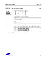
CLMOD
−
−
Clock Output Mode Control Register
FD0H
Bit
Identifier
RESET
Value
Read/Write
Bit Addressing
CLMOD.3
W
4
0
3
.3
Register ID
Register name
Register location
in RAM bank 15
Bit number in
MSB to LSB order
Bit identifier used
for bit addressing
Bit value immediately
following a
RESET
Type of addressing
that must be used to
address the bit
(1-bit, 4-bit, or 8-bit)
R = Read-only
W = Write-only
R/W = Read/write
Register and bit IDs
used for bit addressing
Description of the
effect of specific
bit
Name of individual
bit or related bits
W
0
2
.2
4
W
0
1
.1
4
W
0
0
.0
4
CLMOD.2
CLMOD.1 - .0
Associated
hardware module
CPU
Bit 2
0
Always logic zero
Enable/Disable Clock Output Control Bit
0
1
Disable clock output
Enable clock output
Clock Source and Frequency Selection Control Bits
Select CPU clock source
Select system clock fxx/8 (524 kHz at 4.19 MHz)
0
0
1
1
0
1
0
1
Select system clock fxx/64 (65.5 kHz at 4.19
Select system clock fxx/16 (262 kHz at 4.19
Figure 4-1. Register Description Format
Summary of Contents for KS57C2308
Page 30: ...ADDRESS SPACES KS57C2308 P2308 C2316 P2316 2 22 NOTES ...
Page 168: ...SAM47 INSTRUCTION SET KS57C2308 P2308 C2316 P2316 5 94 NOTES ...
Page 170: ......
Page 206: ...POWER DOWN KS57C2308 P2308 C2316 P2316 8 8 NOTES ...
Page 210: ...RESET KS57C2308 P2308 C2316 P2316 9 4 NOTES ...
Page 222: ...I O PORTS KS57C2308 P2308 C2316 P2316 10 12 NOTES ...
Page 272: ...LCD CONTROLLER DRIVER KS57C2308 P2308 C2316 P2316 12 24 NOTES ...
Page 280: ...SERIAL I O INTERFACE KS57C2308 P2308 C2316 P2316 13 8 NOTES ...
Page 294: ...MECHANICAL DATA KS57C2308 P2308 C2316 P2316 15 2 NOTES ...
Page 310: ...KS57P2308 P2316 OTP KS57C2308 P2308 C2316 P2316 16 16 NOTES ...
Page 318: ......
Page 320: ......
Page 322: ......
Page 325: ......
Page 327: ......


