background image

4-14 

4. Troubleshooting

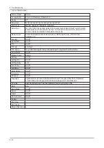
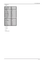
Option Table(Service)

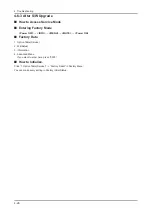
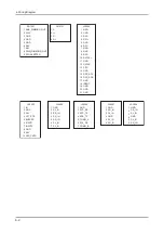
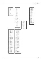
Factory Reset

Default

Country(0x55)

Others-0~3/Russia-4~5/Nordic-6~9

Ready

Off

Panel Inch

19”/22”/23”/26”/27”/32”/37”/40”/42”/46”/50”/52”/57”

Dimm Type

INT/INT_NEG/EXT_POS/EXT_NEG/EXT

Panel Type

19A T/22A T/22D T/26A AG/26L AG/26D T/32L AG/32L NG/32D NG/32D AG/37L AG/37I NG/40L 

AG/40A AG/32A AG 7/32A AG 8/37L NG/26 D T NF/32D AG NF/32A AG NF/37L NG NF/37I NG 

NF/40L AG NF/40A AG NF/32A PB/26A PB/37L PB/40A PB

Model Option

Amber/Coral/Jade/Tanzanite/Hanaro/Jade_FBE/Pyrope/Pyrope_3D/Carnelian/ 

Carnelian_3D

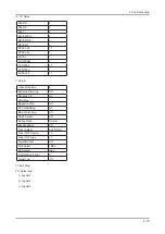
On/Off

Light Effect

On/Off

TTX

On/Off

TTX List

FLOF/List

TTX Group

Lang OSD/W Europe/E Europe/Russia/Greek/Turkey/Arab/Farsi/ArabHbrw

Carrier Mute

On/Off

Volume Curve

EU/EA

HotPlug

On/Off

HotPlugCtrl

On/Off

HotPlugDelay

0~63

Auto Power

On/Off

LNA Menu

On/Off

Hotel Option

On/Off

D.Gamma

On/Off

PC Ident

On/Off

Language

English/Germany/French/Italia/Spain/Netherland/Portuguese/Greek/Czech/Serbian/

Croatian/Romanian/Hungarian/Polish/Russian/Bulgarian/Turkish/Slovakia

Ch Table

SUWON/SESK/SHE/TTSEC/SEIN/SDMA/TSED/SAVINA/SIEL/TSE

DDR

Etron

Shop Mode

On/Off

Nordic

On/Off

Arabic

On/Off

NT Conversion

On/Off

Control
PDP Filter
PDP Group
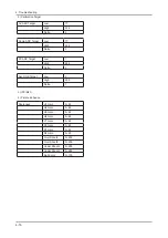
Spread Spectrum

1.

Summary of Contents for LE19A65 A Series

Page 1: ...ICE Manual TFT LCD TV Contents LE19A65 A LE22A65 A Refer to the service manual in the GSPN see the rear cover for the more information 1 Precautions 2 Product specifications 3 Disassembly and Reassembly 4 Troubleshooting 5 Exploded View Part List 6 Wiring Diagram ...

Page 2: ...nd Reassemble 3 1 3 1 Disassembly 3 1 4 Troubleshooting 4 1 4 1 Troubleshooting 4 1 4 2 Alignments and Adjustments 4 11 4 3 Factory Mode Adjustments 4 12 4 4 White Balance Calibration 4 20 4 5 White Ratio Balance Adjustment 4 22 4 6 HOW TO UPGRADE 4 23 5 Exploded View Part List 5 1 5 1 LE19A656A Exploded View 5 1 5 2 LE22A656A Exploded View 5 3 5 3 LE19A656A Parts List 5 5 5 4 LE22A656A Parts List...

Page 3: ...urope samsungportal com China http china samsungportal com Asia http asia samsungportal com Mideast Africa http mea samsungportal com This Service Manual is a property of Samsung Electronics Co Ltd Any unauthorized use of Manual can be punished under applicable International and or domestic law 2008 Samsung Electronics Co Ltd All rights reserved Printed in Korea P N BN82 00378A 00 ...

Page 4: ...tains electrostatically sensitive devices Use caution when handling these components 3 1 Disassembly Cautions 1 Disconnect the monitor from the power source before disassembly 2 Follow these directions carefully never use metal instruments to pry apart the cabinet Description Picture Description Screws 1 Place monitor face down on cushioned table Remove the screws from the Stand Remove stand x 7 x...

Page 5: ...3 2 3 Disassembly and Reassemble Description Picture Description Screws 2 Lift up rear cover and remove the stand 3 Remove Screw from the stand BRKT and lift up the stand BRKT x 2 ...

Page 6: ...3 3 3 Disassembly and Reassemble Description Picture Description Screws 4 Disonnect cable from the boards 5 Remove the screws of Scaler board s shield case and boards x 8 x 1 ...

Page 7: ...3 4 3 Disassembly and Reassemble Description Picture Description Screws 6 Remove screws and Lift up the Lod pa x 4 Reassembly procedures are in the reverse order of disassembly procedures ...

Page 8: ...5 1 5 Exploded View Part List 5 Exploded View Part List 5 1 LE19A650A Exploded View T0003 T0175 M0215 M0014 T0447 M0174 M0027 M0107 M0013 ...

Page 9: ...148B ASSY COVER P FRONT 19 L650 EO READY PM 1 S A M0215 BN07 00462A LCD PANEL M190A1 L07 1 S A T0175 BN96 06823A ASSY SPEAKER P 16ohm CORAL LCD 22 19 3 1 S A M0014 BN94 01818C ASSY PCB MAIN LE19A650A1X CIS 1 S A M0013 BN96 07438B ASSY COVER P REAR 19 L650 EO READY ABS 1 S A M0027 BN96 04794C ASSY STAND P BASE AMBER 19 ABS PMMA HB R 1 S A ...

Page 10: ...5 3 5 Exploded View Part List 5 2 LE22A650A Exploded View T0003 T0175 M0215 T0447 M0013 M0014 M0107 M0174 M0027 ...

Page 11: ... READY PM 1 S A M0215 BN07 00487A LCD PANEL LTM220M1 L01 2 1 S A T0175 BN96 06823A ASSY SPEAKER P 16ohm CORAL LCD 22 19 3 1 S A M0115 BN61 02947A BRACKET STAND LINK JASMINE 32 SECC T1 6 1 S A M0014 BN94 01818D ASSY PCB MAIN LE22A650A1X CIS 1 S A M0013 BN96 07439B ASSY COVER P REAR 22 L650 EO READY ABS 1 S A M0027 BN96 06463C ASSY STAND P BASE AMBER 22 ABS PMMA HB R 1 S A ...

Page 12: ... A 3 CCM1 BN63 02183D COVER SHEET Rhcm PE Vinyl T0 05 680mm 20 0 45 S N A 3 M0006 BN63 04360B COVER REAR 19 L650 EO READY ABS PMMA HB 1 S N A 3 T0071 BN64 00840C INLAY TERMINAL 22L650 EO READY PS SHEET 1 S N A 3 T0064 BN65 00002A CLAMPER CORE BORDEAUX LDPE BLK 1 S N A 3 T0069 BN60 00027C SPACER FELT 19R7 FELT 90 T0 35 10 2 S N A 3 M0113 BN61 02621A BRACKET VESA 19R7 SECC T1 0 2 S N A 0 1 M0001 BN9...

Page 13: ...02691 JACK PIN 2P Ni WHT RED STRAIGHT 1 S A 3 JA333 3722 002703 JACK PIN 3P Ni GRN BLU RED STRAIGHT 1 S A 3 CIS3 BN40 00099A TUNER HTM 6C 235S HTM 6C 235S PAL BG DK 1 S A 3 M0107 BN63 01847A SHIELD COVER ROME SPTE T0 3 49 5 79 5 HE 1 S N A 3 HDCP BN97 00688A ASSY HDCP BN46 00018A PS 42V6S D73A GENE 1 S N A 4 BN46 00018A KEY CODE CERTIFICATE HDCP KEY PPM42M5S 1 S N A 3 T0174 BN97 02209A ASSY SMD LE...

Page 14: ... S A 4 D1005 0403 001425 DIODE ZENER BZX84C33 31 35V 350mW SOT 23 1 S A 4 D0254 0404 001271 DIODE SCHOTTKY SSA34 40V 3000mA SMA TP 1 S A 4 D3053 0406 001172 DIODE TVS CDS3C30GTH 48 50V SMD 1 S A 4 D3054 0406 001172 DIODE TVS CDS3C30GTH 48 50V SMD 1 S A 4 D3055 0406 001172 DIODE TVS CDS3C30GTH 48 50V SMD 1 S A 4 D3056 0406 001172 DIODE TVS CDS3C30GTH 48 50V SMD 1 S A 4 D3057 0406 001172 DIODE TVS C...

Page 15: ...S A 4 Q409 0505 000110 FET SILICON 2N7002 N 60V 115mA 7 5ohm 0 1 S A 4 Q409 0505 000110 FET SILICON 2N7002 N 60V 115mA 7 5ohm 0 1 S A 4 Q409 0505 000110 FET SILICON 2N7002 N 60V 115mA 7 5ohm 0 1 S A 4 Q409 0505 000110 FET SILICON 2N7002 N 60V 115mA 7 5ohm 0 1 S A 4 Q409 0505 001170 FET SILICON SI9933ADY T1 P 20V 3 4A 0 0 1 S A 4 Q409 0505 001170 FET SILICON SI9933ADY T1 P 20V 3 4A 0 0 1 S A 4 IC20...

Page 16: ... A 4 R110 2007 000138 R CHIP 100ohm 5 1 16W TP 1005 1 S N A 4 R110 2007 000138 R CHIP 100ohm 5 1 16W TP 1005 1 S N A 4 R110 2007 000138 R CHIP 100ohm 5 1 16W TP 1005 1 S N A 4 R110 2007 000138 R CHIP 100ohm 5 1 16W TP 1005 1 S N A 4 R110 2007 000138 R CHIP 100ohm 5 1 16W TP 1005 1 S N A 4 R110 2007 000138 R CHIP 100ohm 5 1 16W TP 1005 1 S N A 4 R110 2007 000138 R CHIP 100ohm 5 1 16W TP 1005 1 S N ...

Page 17: ...5 1 S N A 4 R110 2007 000140 R CHIP 1Kohm 5 1 16W TP 1005 1 S N A 4 R110 2007 000140 R CHIP 1Kohm 5 1 16W TP 1005 1 S N A 4 R110 2007 000141 R CHIP 2 2Kohm 5 1 16W TP 1005 1 S N A 4 R110 2007 000141 R CHIP 2 2Kohm 5 1 16W TP 1005 1 S N A 4 R110 2007 000141 R CHIP 2 2Kohm 5 1 16W TP 1005 1 S N A 4 R110 2007 000141 R CHIP 2 2Kohm 5 1 16W TP 1005 1 S N A 4 R110 2007 000141 R CHIP 2 2Kohm 5 1 16W TP 1...

Page 18: ... TP 1005 1 S A 4 R110 2007 000148 R CHIP 10Kohm 5 1 16W TP 1005 1 S A 4 R110 2007 000148 R CHIP 10Kohm 5 1 16W TP 1005 1 S A 4 R110 2007 000148 R CHIP 10Kohm 5 1 16W TP 1005 1 S A 4 R110 2007 000148 R CHIP 10Kohm 5 1 16W TP 1005 1 S A 4 R110 2007 000148 R CHIP 10Kohm 5 1 16W TP 1005 1 S A 4 R110 2007 000148 R CHIP 10Kohm 5 1 16W TP 1005 1 S A 4 R110 2007 000148 R CHIP 10Kohm 5 1 16W TP 1005 1 S A ...

Page 19: ...5 1 16W TP 1005 1 S A 4 R110 2007 000157 R CHIP 47Kohm 5 1 16W TP 1005 1 S A 4 R110 2007 000162 R CHIP 100Kohm 5 1 16W TP 1005 1 S A 4 R110 2007 000162 R CHIP 100Kohm 5 1 16W TP 1005 1 S A 4 R110 2007 000162 R CHIP 100Kohm 5 1 16W TP 1005 1 S A 4 R110 2007 000162 R CHIP 100Kohm 5 1 16W TP 1005 1 S A 4 R110 2007 000162 R CHIP 100Kohm 5 1 16W TP 1005 1 S A 4 R110 2007 000162 R CHIP 100Kohm 5 1 16W T...

Page 20: ...P 1005 1 S A 4 R110 2007 000171 R CHIP 0ohm 5 1 16W TP 1005 1 S A 4 R110 2007 000171 R CHIP 0ohm 5 1 16W TP 1005 1 S A 4 R110 2007 000171 R CHIP 0ohm 5 1 16W TP 1005 1 S A 4 R110 2007 000171 R CHIP 0ohm 5 1 16W TP 1005 1 S A 4 R110 2007 000171 R CHIP 0ohm 5 1 16W TP 1005 1 S A 4 R110 2007 000171 R CHIP 0ohm 5 1 16W TP 1005 1 S A 4 R110 2007 000171 R CHIP 0ohm 5 1 16W TP 1005 1 S A 4 R110 2007 0001...

Page 21: ...R CHIP 39Kohm 5 1 16W TP 1005 1 S A 4 R110 2007 000932 R CHIP 470ohm 5 1 16W TP 1005 1 S N A 4 R110 2007 000932 R CHIP 470ohm 5 1 16W TP 1005 1 S N A 4 R110 2007 000932 R CHIP 470ohm 5 1 16W TP 1005 1 S N A 4 R110 2007 000932 R CHIP 470ohm 5 1 16W TP 1005 1 S N A 4 R110 2007 000932 R CHIP 470ohm 5 1 16W TP 1005 1 S N A 4 R110 2007 000932 R CHIP 470ohm 5 1 16W TP 1005 1 S N A 4 R110 2007 000950 R C...

Page 22: ...R110 2007 002425 R CHIP 1ohm 5 1 10W TP 1608 1 S A 4 R110 2007 002425 R CHIP 1ohm 5 1 10W TP 1608 1 S A 4 R110 2007 002425 R CHIP 1ohm 5 1 10W TP 1608 1 S A 4 R110 2007 007107 R CHIP 100Kohm 1 1 16W TP 1005 1 S N A 4 R110 2007 007107 R CHIP 100Kohm 1 1 16W TP 1005 1 S N A 4 R110 2007 007136 R CHIP 4 7Kohm 1 1 16W TP 1005 1 S N A 4 R110 2007 007141 R CHIP 240ohm 5 1 16W TP 1005 1 S N A 4 R110 2007 ...

Page 23: ...RK 100ohm 5 1 16W L CHIP 8P TP 3 1 S A 4 RA5028 2011 001093 R NETWORK 100ohm 5 1 16W L CHIP 8P TP 3 1 S A 4 RA5029 2011 001093 R NETWORK 100ohm 5 1 16W L CHIP 8P TP 3 1 S A 4 RA5032 2011 001093 R NETWORK 100ohm 5 1 16W L CHIP 8P TP 3 1 S A 4 RA5033 2011 001093 R NETWORK 100ohm 5 1 16W L CHIP 8P TP 3 1 S A 4 C120 2203 000233 C CER CHIP 0 1nF 5 50V C0G 1005 1 S A 4 C120 2203 000233 C CER CHIP 0 1nF ...

Page 24: ... C CER CHIP 22nF 10 50V X7R 1608 1 S A 4 C120 2203 002398 C CER CHIP 22nF 10 50V X7R 1608 1 S A 4 C120 2203 002398 C CER CHIP 22nF 10 50V X7R 1608 1 S A 4 C120 2203 002525 C CER CHIP 0 56nF 10 50V X7R TP 1005 1 S N A 4 C120 2203 002525 C CER CHIP 0 56nF 10 50V X7R TP 1005 1 S N A 4 C120 2203 002525 C CER CHIP 0 56nF 10 50V X7R TP 1005 1 S N A 4 C120 2203 002525 C CER CHIP 0 56nF 10 50V X7R TP 1005...

Page 25: ... 4 C120 2203 005809 C CER CHIP 1000nF 10 16V X7R 2012 1 S A 4 C120 2203 005809 C CER CHIP 1000nF 10 16V X7R 2012 1 S A 4 C120 2203 005809 C CER CHIP 1000nF 10 16V X7R 2012 1 S A 4 C120 2203 005809 C CER CHIP 1000nF 10 16V X7R 2012 1 S A 4 C120 2203 005809 C CER CHIP 1000nF 10 16V X7R 2012 1 S A 4 C120 2203 005809 C CER CHIP 1000nF 10 16V X7R 2012 1 S A 4 C120 2203 005809 C CER CHIP 1000nF 10 16V X...

Page 26: ...006361 C CER CHIP 10000nF 10 10V X5R 2012 1 S A 4 C120 2203 006361 C CER CHIP 10000nF 10 10V X5R 2012 1 S A 4 C120 2203 006361 C CER CHIP 10000nF 10 10V X5R 2012 1 S A 4 C120 2203 006361 C CER CHIP 10000nF 10 10V X5R 2012 1 S A 4 C120 2203 006361 C CER CHIP 10000nF 10 10V X5R 2012 1 S A 4 C120 2203 006361 C CER CHIP 10000nF 10 10V X5R 2012 1 S A 4 C120 2203 006361 C CER CHIP 10000nF 10 10V X5R 201...

Page 27: ...0 2203 006681 C CER CHIP 100nF 80 20 25V Y5V 1005 1 S N A 4 C120 2203 006681 C CER CHIP 100nF 80 20 25V Y5V 1005 1 S N A 4 C120 2203 006681 C CER CHIP 100nF 80 20 25V Y5V 1005 1 S N A 4 C120 2203 006681 C CER CHIP 100nF 80 20 25V Y5V 1005 1 S N A 4 C120 2203 006681 C CER CHIP 100nF 80 20 25V Y5V 1005 1 S N A 4 C120 2203 006681 C CER CHIP 100nF 80 20 25V Y5V 1005 1 S N A 4 C120 2203 006681 C CER CH...

Page 28: ...00nF 10 16V X5R TP 2012 1 S N A 4 C120 2203 007176 C CER CHIP 10000nF 10 16V X5R TP 2012 1 S N A 4 C120 2203 007176 C CER CHIP 10000nF 10 16V X5R TP 2012 1 S N A 4 C120 2203 007176 C CER CHIP 10000nF 10 16V X5R TP 2012 1 S N A 4 C120 2203 007176 C CER CHIP 10000nF 10 16V X5R TP 2012 1 S N A 4 C120 2203 007176 C CER CHIP 10000nF 10 16V X5R TP 2012 1 S N A 4 C120 2203 007176 C CER CHIP 10000nF 10 16...

Page 29: ...1236 BEAD SMD 60ohm 1608 1 S N A 4 T0568 3301 001236 BEAD SMD 60ohm 1608 1 S N A 4 T0568 3301 001324 BEAD SMD 15ohm 2012 600mA TP 0 1ohm 1 S A 4 T0568 3301 001324 BEAD SMD 15ohm 2012 600mA TP 0 1ohm 1 S A 4 T0568 3301 001324 BEAD SMD 15ohm 2012 600mA TP 0 1ohm 1 S A 4 T0568 3301 001324 BEAD SMD 15ohm 2012 600mA TP 0 1ohm 1 S A 4 T0568 3301 001324 BEAD SMD 15ohm 2012 600mA TP 0 1ohm 1 S A 4 T0568 3...

Page 30: ...R WALL POSITION COMM SAMSUNG 1 S N A 3 BN68 00850H MANUAL FLYER WALL MOUNT COMM SAMSUNG Eng 1 S N A 3 M0132 BN96 01272A ASSY MISC P SCREW VE15UO 1 S N A 3 6902 000128 BAG ZIPPER LDPE T0 05 W200 L150 TRP 8 2 1 S N A 3 T0101 BN61 01162A BRACKET WALL VE15 SECC 2 0 1 S N A 0 1 M0019 BN92 03478A ASSY LABEL LE19A650A1XXC 1 S N A 0 1 M0003 BN92 03496D ASSY BOX 19AA1 EO AMBER 1 S N A 2 BN69 02632A BOX 01 ...

Page 31: ... BOSS TAPE AMBER ACRYL T1 1 W8 0mm WHITE 0 6 S N A 3 H BOSS B BN61 03261M BOSS TAPE AMBER ACRYL T1 1 W16 0mm WHITE 0 6 S N A 3 M0175 BN96 08120F ASSY BOARD P TOUCH FUNCTION IR LN22A650A 1 S N A 0 1 M0002 BN90 01673B ASSY COVER REAR 22 L650 EO READY 1 S N A 2 T0081 6002 001294 SCREW TAPPING BH M4 L16 ZPC BLK 7 S A 2 M0013 BN96 07439B ASSY COVER P REAR 22 L650 EO READY ABS 1 S A 3 T0069 AA63 60122D ...

Page 32: ... 235S HTM 6C 235S PAL BG DK 1 S A 3 M0107 BN63 01847A SHIELD COVER ROME SPTE T0 3 49 5 79 5 HE 1 S N A 3 HDCP BN97 00688A ASSY HDCP BN46 00018A PS 42V6S D73A GENE 1 S N A 4 BN46 00018A KEY CODE CERTIFICATE HDCP KEY PPM42M5S 1 S N A 3 T0174 BN97 02209B ASSY SMD LE22A650A1XXC 1 S N A 4 SUB05 0202 001477 SOLDER CREAM LST309 M D20 45um 96 5Sn 1 574 S N A 4 D2012 0401 000133 DIODE SWITCHING RLS4148 75V...

Page 33: ... A 4 D3053 0406 001172 DIODE TVS CDS3C30GTH 48 50V SMD 1 S A 4 D3054 0406 001172 DIODE TVS CDS3C30GTH 48 50V SMD 1 S A 4 D3055 0406 001172 DIODE TVS CDS3C30GTH 48 50V SMD 1 S A 4 D3056 0406 001172 DIODE TVS CDS3C30GTH 48 50V SMD 1 S A 4 D3057 0406 001172 DIODE TVS CDS3C30GTH 48 50V SMD 1 S A 4 D3058 0406 001172 DIODE TVS CDS3C30GTH 48 50V SMD 1 S A 4 D3068 0406 001172 DIODE TVS CDS3C30GTH 48 50V S...

Page 34: ...ohm 0 1 S A 4 Q409 0505 000110 FET SILICON 2N7002 N 60V 115mA 7 5ohm 0 1 S A 4 Q409 0505 000110 FET SILICON 2N7002 N 60V 115mA 7 5ohm 0 1 S A 4 Q409 0505 001170 FET SILICON SI9933ADY T1 P 20V 3 4A 0 0 1 S A 4 Q409 0505 001170 FET SILICON SI9933ADY T1 P 20V 3 4A 0 0 1 S A 4 IC2002 1001 000164 IC ANALOG MULTIPLEX 74HC4052 CMOS SOP 16 1 S A 4 IC112 1103 000129 IC EEPROM 24C02 2Kbit 256x8Bit SOP 8P 5x...

Page 35: ... N A 4 R110 2007 000138 R CHIP 100ohm 5 1 16W TP 1005 1 S N A 4 R110 2007 000138 R CHIP 100ohm 5 1 16W TP 1005 1 S N A 4 R110 2007 000138 R CHIP 100ohm 5 1 16W TP 1005 1 S N A 4 R110 2007 000138 R CHIP 100ohm 5 1 16W TP 1005 1 S N A 4 R110 2007 000138 R CHIP 100ohm 5 1 16W TP 1005 1 S N A 4 R110 2007 000138 R CHIP 100ohm 5 1 16W TP 1005 1 S N A 4 R110 2007 000138 R CHIP 100ohm 5 1 16W TP 1005 1 S ...

Page 36: ...5 1 S N A 4 R110 2007 000141 R CHIP 2 2Kohm 5 1 16W TP 1005 1 S N A 4 R110 2007 000141 R CHIP 2 2Kohm 5 1 16W TP 1005 1 S N A 4 R110 2007 000141 R CHIP 2 2Kohm 5 1 16W TP 1005 1 S N A 4 R110 2007 000141 R CHIP 2 2Kohm 5 1 16W TP 1005 1 S N A 4 R110 2007 000141 R CHIP 2 2Kohm 5 1 16W TP 1005 1 S N A 4 R110 2007 000141 R CHIP 2 2Kohm 5 1 16W TP 1005 1 S N A 4 R110 2007 000141 R CHIP 2 2Kohm 5 1 16W ...

Page 37: ... TP 1005 1 S A 4 R110 2007 000148 R CHIP 10Kohm 5 1 16W TP 1005 1 S A 4 R110 2007 000148 R CHIP 10Kohm 5 1 16W TP 1005 1 S A 4 R110 2007 000148 R CHIP 10Kohm 5 1 16W TP 1005 1 S A 4 R110 2007 000148 R CHIP 10Kohm 5 1 16W TP 1005 1 S A 4 R110 2007 000148 R CHIP 10Kohm 5 1 16W TP 1005 1 S A 4 R110 2007 000148 R CHIP 10Kohm 5 1 16W TP 1005 1 S A 4 R110 2007 000148 R CHIP 10Kohm 5 1 16W TP 1005 1 S A ...

Page 38: ...Kohm 5 1 16W TP 1005 1 S A 4 R110 2007 000162 R CHIP 100Kohm 5 1 16W TP 1005 1 S A 4 R110 2007 000162 R CHIP 100Kohm 5 1 16W TP 1005 1 S A 4 R110 2007 000162 R CHIP 100Kohm 5 1 16W TP 1005 1 S A 4 R110 2007 000162 R CHIP 100Kohm 5 1 16W TP 1005 1 S A 4 R110 2007 000162 R CHIP 100Kohm 5 1 16W TP 1005 1 S A 4 R110 2007 000162 R CHIP 100Kohm 5 1 16W TP 1005 1 S A 4 R110 2007 000162 R CHIP 100Kohm 5 1...

Page 39: ... 1005 1 S A 4 R110 2007 000171 R CHIP 0ohm 5 1 16W TP 1005 1 S A 4 R110 2007 000171 R CHIP 0ohm 5 1 16W TP 1005 1 S A 4 R110 2007 000171 R CHIP 0ohm 5 1 16W TP 1005 1 S A 4 R110 2007 000171 R CHIP 0ohm 5 1 16W TP 1005 1 S A 4 R110 2007 000171 R CHIP 0ohm 5 1 16W TP 1005 1 S A 4 R110 2007 000171 R CHIP 0ohm 5 1 16W TP 1005 1 S A 4 R110 2007 000171 R CHIP 0ohm 5 1 16W TP 1005 1 S A 4 R110 2007 00017...

Page 40: ...32 R CHIP 470ohm 5 1 16W TP 1005 1 S N A 4 R110 2007 000932 R CHIP 470ohm 5 1 16W TP 1005 1 S N A 4 R110 2007 000932 R CHIP 470ohm 5 1 16W TP 1005 1 S N A 4 R110 2007 000932 R CHIP 470ohm 5 1 16W TP 1005 1 S N A 4 R110 2007 000950 R CHIP 47ohm 5 1 4W TP 3216 1 S A 4 R110 2007 000950 R CHIP 47ohm 5 1 4W TP 3216 1 S A 4 R110 2007 000950 R CHIP 47ohm 5 1 4W TP 3216 1 S A 4 R110 2007 000950 R CHIP 47o...

Page 41: ...100Kohm 1 1 16W TP 1005 1 S N A 4 R110 2007 007107 R CHIP 100Kohm 1 1 16W TP 1005 1 S N A 4 R110 2007 007136 R CHIP 4 7Kohm 1 1 16W TP 1005 1 S N A 4 R110 2007 007141 R CHIP 240ohm 5 1 16W TP 1005 1 S N A 4 R110 2007 007319 R CHIP 390ohm 1 1 16W TP 1005 1 S N A 4 R110 2007 007334 R CHIP 200Kohm 1 1 16W TP 1005 1 S N A 4 R110 2007 007735 R CHIP 91ohm 1 1 10W TP 1608 1 S A 4 R110 2007 007791 R CHIP ...

Page 42: ...01093 R NETWORK 100ohm 5 1 16W L CHIP 8P TP 3 1 S A 4 RA5033 2011 001093 R NETWORK 100ohm 5 1 16W L CHIP 8P TP 3 1 S A 4 C120 2203 000233 C CER CHIP 0 1nF 5 50V C0G 1005 1 S A 4 C120 2203 000233 C CER CHIP 0 1nF 5 50V C0G 1005 1 S A 4 C120 2203 000233 C CER CHIP 0 1nF 5 50V C0G 1005 1 S A 4 C120 2203 000233 C CER CHIP 0 1nF 5 50V C0G 1005 1 S A 4 C120 2203 000233 C CER CHIP 0 1nF 5 50V C0G 1005 1 ...

Page 43: ...CER CHIP 0 56nF 10 50V X7R TP 1005 1 S N A 4 C120 2203 002525 C CER CHIP 0 56nF 10 50V X7R TP 1005 1 S N A 4 C120 2203 002525 C CER CHIP 0 56nF 10 50V X7R TP 1005 1 S N A 4 C120 2203 002525 C CER CHIP 0 56nF 10 50V X7R TP 1005 1 S N A 4 C120 2203 002525 C CER CHIP 0 56nF 10 50V X7R TP 1005 1 S N A 4 C120 2203 002525 C CER CHIP 0 56nF 10 50V X7R TP 1005 1 S N A 4 C120 2203 002525 C CER CHIP 0 56nF ...

Page 44: ... A 4 C120 2203 005809 C CER CHIP 1000nF 10 16V X7R 2012 1 S A 4 C120 2203 005809 C CER CHIP 1000nF 10 16V X7R 2012 1 S A 4 C120 2203 005809 C CER CHIP 1000nF 10 16V X7R 2012 1 S A 4 C120 2203 005809 C CER CHIP 1000nF 10 16V X7R 2012 1 S A 4 C120 2203 005809 C CER CHIP 1000nF 10 16V X7R 2012 1 S A 4 C120 2203 005968 C CER CHIP 4 7NF 10 50V X7R TP 1005 1 S N A 4 C120 2203 005968 C CER CHIP 4 7NF 10 ...

Page 45: ...361 C CER CHIP 10000nF 10 10V X5R 2012 1 S A 4 C120 2203 006361 C CER CHIP 10000nF 10 10V X5R 2012 1 S A 4 C120 2203 006361 C CER CHIP 10000nF 10 10V X5R 2012 1 S A 4 C120 2203 006361 C CER CHIP 10000nF 10 10V X5R 2012 1 S A 4 C120 2203 006361 C CER CHIP 10000nF 10 10V X5R 2012 1 S A 4 C120 2203 006361 C CER CHIP 10000nF 10 10V X5R 2012 1 S A 4 C120 2203 006361 C CER CHIP 10000nF 10 10V X5R 2012 1...

Page 46: ...0 2203 006681 C CER CHIP 100nF 80 20 25V Y5V 1005 1 S N A 4 C120 2203 006681 C CER CHIP 100nF 80 20 25V Y5V 1005 1 S N A 4 C120 2203 006681 C CER CHIP 100nF 80 20 25V Y5V 1005 1 S N A 4 C120 2203 006681 C CER CHIP 100nF 80 20 25V Y5V 1005 1 S N A 4 C120 2203 006681 C CER CHIP 100nF 80 20 25V Y5V 1005 1 S N A 4 C120 2203 006681 C CER CHIP 100nF 80 20 25V Y5V 1005 1 S N A 4 C120 2203 006681 C CER CH...

Page 47: ... CHIP 10000nF 10 16V X5R TP 2012 1 S N A 4 C120 2203 007176 C CER CHIP 10000nF 10 16V X5R TP 2012 1 S N A 4 C120 2203 007176 C CER CHIP 10000nF 10 16V X5R TP 2012 1 S N A 4 C120 2203 007176 C CER CHIP 10000nF 10 16V X5R TP 2012 1 S N A 4 C120 2203 007176 C CER CHIP 10000nF 10 16V X5R TP 2012 1 S N A 4 C3059 2402 001129 C AL SMD 47UF 20 16V WT TP 6 3X5 2MM 1 S A 4 C1025 2402 001238 C AL SMD 1uF 20 ...

Page 48: ...0mA TP 0 1ohm 1 S A 4 T0568 3301 001324 BEAD SMD 15ohm 2012 600mA TP 0 1ohm 1 S A 4 T0568 3301 001324 BEAD SMD 15ohm 2012 600mA TP 0 1ohm 1 S A 4 T0568 3301 001324 BEAD SMD 15ohm 2012 600mA TP 0 1ohm 1 S A 4 T0568 3301 001404 BEAD SMD 30ohm 2012 TP 15 9OHM 30MHz 1 S A 4 T0568 3301 001404 BEAD SMD 30ohm 2012 TP 15 9OHM 30MHz 1 S A 4 T0568 3301 001404 BEAD SMD 30ohm 2012 TP 15 9OHM 30MHz 1 S A 4 T05...

Page 49: ...WARRANTY CARD comm Samsu 1 S N A 2 T0511 BN68 01593A MANUAL USERS COMM SAMSUNG 12Lang W EUROP 1 S N A 0 1 M0019 BN92 03478A ASSY LABEL LE19A650A1XXC 1 S N A 0 1 M0003 BN92 03497D ASSY BOX 22AA1 EO AMBER 1 S N A 2 BN69 02633A BOX 01 SET 22L650 CB A 01 SW 50 YEL W620 1 S N A 0 1 M0113 BN92 03499A ASSY P MATERIAL 22AA1 AMBER 1 S N A 2 T0524 6902 000758 BAG PE HDPE HDPE NITRON T0 015 T0 015 T1 1 S N A...

Page 50: ...tandards Institute ANSI C101 1 Leakage Current for Appliances and Underwriters Laboratories UL Publication UL1410 59 7 With the unit completely reassembled plug the AC line cord directly into a 120V AC outlet With the unit s AC switch first in the ON position and then OFF measure the current between a known earth ground metal water pipe conduit etc and all exposed metal parts including metal cabin...

Page 51: ...ground lead last 1 3 Electrostatically Sensitive Devices ESD Precautions Some semiconductor solid state devices can be easily damaged by static electricity Such components are commonly called Electrostatically Sensitive Devices ESD Examples of typical ESD are integrated circuits and some field effect transistors The following techniques will reduce the incidence of component damage caused by stati...

Page 52: ...om being exposed to moisture Otherwise it may cause a fire or electric shock Make sure to turn the power off and unplug the power cord from the outlet before repositioning the product Also check the antenna cable or the external connectors if they are fully unplugged Damage to the cord may cause fire or electric shock Keep the antenna far away from any high voltage cables and install it firmly Con...

Page 53: ...1 4 1 Precautions Memo ...

Page 54: ...rate TTL P or N Maximum Pixel Clock rate 80MHz Active Display Horizontal Vertical 27 47 x 15 44 inches 697 68 H x 392 26 V mm AC power voltage Frequency AC 110V 240V 50 60Hz Power Consumption 50 W 1W stand by Dimensions 18 90 x 7 09 x 15 59 inches 480 0 x 180 2 x 396 0 mm with stand 18 90 x 2 34 x 13 98 inches 480 0 x 59 5 x 355 0 mm without stand Set W x D x H Weight Set 12 35 lbs 5 6Kg TV System...

Page 55: ...lock rate 80MHz Active Display Horizontal Vertical 473 76 H x 296 1 V mm AC power voltage Frequency AC 110V 240V 50 60Hz Power Consumption 60 W 1W stand by Dimensions 22 14 x 8 50 x 17 8 inches 562 4 x 216 x 452 2 mm with stand 22 14 x 8 50 x 15 85 inches 562 4 x 216 x 402 6mm without stand Set W x D x H Weight Set 15 87lbs 7 2Kg TV System Tuning Frequency Synthesize Refer to detailed Frequency Ta...

Page 56: ...7 585 25 UHF T 277 25 SUPER T 276 00 T 277 25 34 34 593 591 25 UHF U 283 25 SUPER U 282 00 U 283 25 35 35 599 597 25 UHF V 289 25 SUPER V 288 00 V 289 25 36 36 605 603 25 UHF W 295 25 SUPER W 294 00 W 295 25 37 37 611 609 25 UHF AA 301 25 HYPER AA 300 00 AA 301 25 38 38 617 615 25 UHF BB 307 25 HYPER BB 306 00 BB 307 25 39 39 623 621 25 UHF CC 313 25 HYPER CC 312 00 CC 313 25 40 40 629 627 25 UHF ...

Page 57: ...9 25 91 91 91 625 25 ULTRA 91 624 00 91 625 25 92 92 92 631 25 ULTRA 92 630 00 92 631 25 93 93 93 637 25 ULTRA 93 636 00 93 637 25 94 94 94 643 25 ULTRA 94 642 00 94 643 25 95 95 A 5 91 25 FM A 5 90 00 A 5 91 25 96 96 A 4 97 25 FM A 4 96 00 A 4 97 25 97 97 A 3 103 25 FM A 3 102 00 A 3 103 25 98 98 A 2 109 25 MID A 2 108 00 A 2 109 25 99 99 A 1 115 25 MID A 1 114 00 A 1 115 25 100 100 100 649 25 UL...

Page 58: ...s with stand 18 90 x 2 34 x 13 98 inches without stand 22 22 14 x 8 50 x 17 80 inches with stand 22 14 x 2 70 x 15 85 inches without stand 22 24 23 x 9 12 x 17 43 inches with stand 24 23 x 3 20 x 15 88 inches without stand 19 18 9 x 7 09 x 15 47 inches with stand 18 9 x 2 26 x 14 19 inches without stand Weight 19 12 35 lbs set 22 15 87 lbs set 22 16 53 lbs set 19 11 46 lbs set Brightness 300 nit 3...

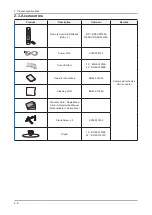
Page 59: ...5A READY BN59 00676A Samsung Electronics Service center Power Cord 3903 000145 Cover Bottom 19 BN63 03039A 22 BN63 04269B Owner s Instructions BN68 01424A Cleaning Cloth BN63 01798A Warranty Card Registration Card Safety Guide Manual Not available in all locations Stand Screw x 4 6002 001294 Stand 19 BN90 01200E 22 BN90 01510C ...

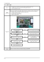
Page 60: ...e various cable connections first Check to see if there is a burnt or damaged cable Check to see if there is a disconnected or loose cable connection Check to see if the cables are connected according to the connection diagram Check the power input to the Main Board 1 2 ...

Page 61: ...ollowing Check the internal cable connection status inside the unit Check the fuses of each part Check the output voltage of SMPS Replace the Main Board Diagnostics Caution Make sure to disconnect the power before working on the SMPS IP Does proper DC 3 3V appear at C1013 Check a IC1011 Change a main PCB ass y No Yes Does proper DC 5V 2 5V 1 2V appear at C1051 C1057 C1066 No Yes LAMP off power ind...

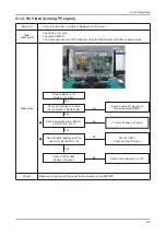
Page 62: ...able Change a PC cable No Does the digital data appear at the output of LVDS RA5012 13 Power Indicator is off Lamp on no video No Check a PC source and check the connection of DSUB cable Check a IC5001 Change a main PCB ass y Yes Does the signal appear at BD3014 3015 3016 R G B Please Call to Samsung Co LTD No Check a LVDS cable Replace a lcd panel Yes Yes Input a analog PC signal and connected ca...

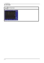
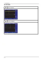
Page 63: ...4 4 4 Troubleshooting WAVEFORMS 1 R G B Output Signal ...

Page 64: ...ing the Main Board and the Panel is disconnected Diagnostics Power Indicator is off Lamp on no video No Check the connection of HDMI cable Check a IC5001 Change a main PCB ass y No Does the digital data appear at the No output of LVDS RA5012 14 No Please Contact Tech support Check the LVDS cable Replace the LCD panel Yes Input a HDMI cable Yes Yes 3 1 Caution Make sure to disconnect the power befo...

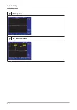
Page 65: ...4 6 4 Troubleshooting WAVEFORMS 2 Digital Output Data 3 Signal of HDMI Data ...

Page 66: ...and the Panel is disconnected Diagnostics No Check a B voltage 3 of Tuner 5V change a main PCB ass y No No Power Indicator is off Lamp on no picure Yes Change a main PCB ass y Does the signal appear at L3001 Does the signal appear at R3169 No Please Call to Samsung Co LTD Check the LVDS cable Replace the LCD panel Yes Connect the RF cable and check RF signal Yes 1 2 Caution Make sure to disconnect...

Page 67: ...4 8 4 Troubleshooting WAVEFORMS 3 CVBS Output Signal 4 Tuner_CVBS Output Signal ...

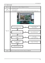
Page 68: ...cted Diagnostics No Check sound cables of each source and a connection harness No Picture is display no sound Check IC2002 Change a main PCB ass y No Does the signal appear at C2058 65 Does the signal appear at 3 13 of IC2002 Change a main PCB ass y No Does the signal appear at BD2006 9 Replace the speaker ass y Yes Connect a sound cable control a volume Yes 1 Yes 3 Yes 2 Caution Make sure to disc...

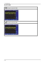
Page 69: ...4 10 4 Troubleshooting WAVEFORMS 6 The Signal are Inputed to IC2002 7 The Signal are Inputed to IC2001 ...

Page 70: ...s essential Avoid overload Excessive signal from a sweep generator might overload the front end of the TV When inserting signal markers do not allow the marker generator to distort test result Connect the TV only to an AC power source with voltage and frequency as specified on the backcover nameplate Do not attempt to connect or disconnect any wire while the TV is turned on Make sure that the powe...

Page 71: ... PICTURE ON FACTORY The buttons are active in the service mode 1 Remote Control Key Power Arrow Up Arrow Down Arrow Left Arrow Right Menu Enter Number Key 0 9 2 Function Control Key Power CH CH VOL VOL Menu TV VIDEO Enter 4 3 2 Panel Check You have to check Panel Maker Because of different adjustments as follows First of all Check the label rating 1 Label Rating File LCD PANEL MARK A ACER AUO S SE...

Page 72: ...ctory Data Option Table Service WB Adjust Information Checksum T AMB22PEUMD XXXX Main Micom Ver T PERLDEUC XXXX DTV MICOM Ver EDID L12_1680_1050 Success IF 19 1440 x 900 HDCP Success Month Day Year Hour Min Sec 4 Advanced Menu 1 2 3 ...

Page 73: ... Pyrope Pyrope_3D Carnelian Carnelian_3D Anynet On Off Light Effect On Off TTX On Off TTX List FLOF List TTX Group Lang OSD W Europe E Europe Russia Greek Turkey Arab Farsi ArabHbrw Carrier Mute On Off Volume Curve EU EA HotPlug On Off HotPlugCtrl On Off HotPlugDelay 0 63 Auto Power On Off LNA Menu On Off Hotel Option On Off D Gamma On Off PC Ident On Off Language English Germany French Italia Spa...

Page 74: ...ess IF 19 1440 x 900 HDCP Success Month Day Year Hour Min Sec 4 Advanced Menu I MST68981 1 ADC Calibration ADC Calibration AV COMP PC HDMI DTV CVBS Y Offs 0 255 CVBS Y Gain 0 255 Ana Y G Offs 0 255 Ana U B Offs 0 255 Ana V R Offs 0 255 Ana Y G Gain 0 255 Ana U B Gain 0 255 Ana V R Gain 0 255 RGB R Offs 0 255 RGB G Offs 0 255 RGB B Offs 0 255 RGB R Gain 0 255 RGB G Gain 0 255 RGB B Gain 0 255 ...

Page 75: ... Delta 3 PC ADC Target Low 1 High 254 Delta 3 ALL RGB Target Low 2 High 235 Delta 1 3 IPC MJC 4 Picture Enhance Sharpness H1 Gain 0 63 H2 Gain 0 63 H3 Gain 0 63 H4 Gain 0 63 V1 Gain 0 63 V2 Gain 0 63 D1 Gain 0 63 D2 Gain 0 63 Over Shoot2 0 255 Over Shoot3 0 255 Under Shoot2 0 255 Under Shoot3 0 255 Sub Color 0 100 ...

Page 76: ... 0 B Slope Gain 45 B Tilt Min 40 B Tilt Max 120 Lfunc Basis 80 Hfunc Basis 85 Mean Offset1 30 Mean Offset2 235 Mean Slope 112 ACR Offset 15 ACR Th1 10 ACR Th2 110 Skin Enable 1 Skin Uv 138 Mskin Uv 140 Sub Color 128 Msub Color 112 2 FRCS 3 FRCM 4 LD 5 PDP LOGIC ...

Page 77: ... Time 8 Ch1BW 2 Ch2BW 1 Num of Check 1 Num of Double Check 5 Mono Weight 1 Stereo Weight 1 Dual Weight 1 BG M2S Threshold 144 DK M2S Threshold 80 BG S2M Threshold 176 DK S2M Threshold 0 FINE Vol 20 Detection Threshold Ext Volume Scale 2 Ext Prescale Speaker 0 R2E Scart2 Offset 2 NTP3000 NTP Master Volume 30 NTP PWM Modulation 239 NTP DRC Thresh 18 NTP Speaker EQ On ...

Page 78: ...Adjust Video Mute time 8 Dynamic Dimming Off Dynamic CE On LNA Plus Megazine LNA Off DTV WatchDog On Main WatchDog Off UART Select Off Debug Mode Normal BackEndMute Off Tuner Select ALPS_Slim Tuner TOP Semco 10 Tuner TOP Alps 13 PixelShift Test Off FBE Select FBE3 Hp Detexct High D WatchDog Count 0 Visual Test Off VI Bus Stop VII Defect Log 1 LogList1 2 LogList2 3 LogList3 ...

Page 79: ...Source HDMI 2 Setting Mode 1280 720 60Hz 3 Pattern Pattern 24 Chess Pattern Chess Pattern 4 Use Equipment CA210 Master MSPG925 Generator Use other equipment only after comparing the result with that of the Master equipment Input mode Calibration Pattern CVBS IN Model_ 2 Perform in PAL B W Pattern 24 Lattice Component IN Model_ 6 Perform in 720p B W Pattern 24 Lattice PC Analog IN Model_ 21 Perform...

Page 80: ...ete it returns to the high level menu 8 You can see the change of the Comp Calibration status from Failure to Success Method of Color Calibration PC 1 Apply the VESA XGA Lattice N0 21 pattern signal to the PC IN port 2 Press the Source key to switch to PC mode 3 Enter Service mode 4 Select the Calibration menu 5 Select the PC Calibration menu 6 In PC Calibration Off status press the key to perform...

Page 81: ...aries with Panel s size and Specification 1 2 3 Equipment CS 210 Pattern MIK K 7256 92 Flat W B Pattern as standard Use other equipment only after comparing the result with that of the Master equipment Set Aging time 60min Calibration and Manual setting for WB adjustment HDMI Time 6 720P Pattern 24 Chessboard Calibration Manual adjustment 92 pattern 720p COMP Time 6 720P Pattern 24 Chessboard Cali...

Page 82: ... 272 278 17 0 cd m2 3 5 Ft Sub_BR 128 12 000 0 HDMI 720P H L 272 278 Sub_CT 140 12 000 0 L L 272 278 17 0 cd m2 5 0 Ft Sub_BR 128 12 000 0 Adjustment Specification White Balance High light 3 Low light 5 Luminance High light 0 1Ft L Low light 0 1Ft L 4 6 HOW TO UPGRADE 4 6 1 ATV S W Order Description ETC 1 Open the Flash Downloader 2 Connect DDC Manager to the TV Set with D SUB Cable ...

Page 83: ...4 24 4 Troubleshooting Order Description ETC 3 Open the Flash Downloader 4 Click Connect Before clicking the icon TV shoud be turned on 5 Click Program ...

Page 84: ...n 2 Open the Samsung Set top Box upgrade Wizard 3 1 Choose the DTV S W by clicking Browse 2 After choosing the S W click the Next icon 4 1 Choose the DTV S W by clicking Browse 2 After choosing the S W click the Next icon It doesn t matter soft or hard power off and on 5 After scaning COM port Model and Version click Next ...

Page 85: ...tory Mode Power OFF INFO MENU MUTE Power ON Factory Data Option Table Service WB Adjust Information Advanced Menu If you want to enter here press 0000 How to Initialize Click 1 Option Table Service Factory Reset in Factory Menu You can make every setting in Factory Initial Status 1 2 3 4 ...

Page 86: ...6 1 6 Wiring Diagram 6 Wiring Diagram 6 1 Wiring Diagram CN1 CN6002 CN304 CN2 CN1001 CN301 CN2 CN3002 CN2101 Driver T CON Function IR Speaker IP Board Main Board ...

Page 87: ... CEC 14 GND 15 DDC_SCL 16 DDC_SDA 17 GND 18 IDENT 19 GND 20 GND 21 GND 1 IR 1 GND 1 GND 1 GND 1 GND 2 GND 2 SL_IN 2 SVC_RX 2 SR_IN 2 SR_IN 3 A5V 3 SR_IN 3 SVC_TX 3 SL_IN 3 SL_IN 4 LET_STB 4 SR_IN 4 SDA_TX 4 GND 4 GND 5 BUZZER 5 SR_IN 5 COMM_A 5 SL_IN 5 SL_IN 6 INPUT1 6 SL_IN 6 SCL_RX 6 SR_IN 6 SR_IN 7 INPUT2 7 SL_IN 7 COMM_B 8 GND 9 A5V 10 LED_CNTR JA3002 CN3002 JA3005 JA3006 JA3007 JA3008 CN1001 ...

Page 88: ...PANEL_VCC 2 ODD_TX0 3 PANEL_VCC 3 ODD_TX1 4 NC 4 ODD_TX1 5 NC 5 ODD_TX2 6 NC 6 ODD_TX2 7 GND 7 GND 8 EVEN_TX3 8 ODD_TXCLK 9 EVEN_TX3 9 ODD_TXCLK 10 EVEN_TXCLK 10 ODD_TX3 11 EVEN_TXCLK 11 ODD_TX3 12 EVEN_TX2 12 EVEN_TX0 13 EVEN_TX2 13 EVEN_TX0 14 GND 14 GND 15 EVEN_TX1 15 EVEN_TX2 16 EVEN_TX2 16 EVEN_TX1 17 GND 17 GND 18 EVEN_TX0 18 EVEN_TX2 19 EVEN_TX0 19 EVEN_TX2 20 ODD_TX3 20 EVEN_TXCLK 21 ODD_T...

Page 89: ...6 4 6 Wiring Diagram 6 2 Wiring Picture 6 2 1 LE19A656A 6 2 2 LE19A651A ...

Page 90: ...6 5 6 Wiring Diagram 6 2 3 LE22A656A 6 2 4 LE19A651A ...

Page 91: ...e CN3002 Function IR Connection Main Board and Function IR Assy defective symptom Control panel remocon doesn t work CN6002_DIP T CON The LVDS signal transferred from Main Board to Panel defective symptom No picture but panel on CN1 CN2 Panel CN304 3 CN301 2 IP Board Supply power and signal from SMPS to Inverter defective symptom No picture but normal sound ...

Page 92: ...6 7 6 Wiring Diagram 6 4 Cables Code BN39 00953D 30P 200mm Photo ...

Page 93: ...6 8 6 Wiring Diagram Memo ...

Reviews: