background image

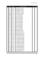
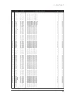
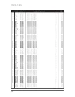
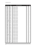
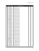
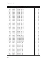
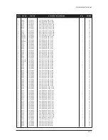
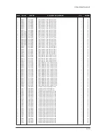
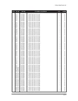
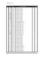
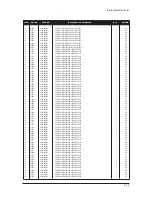
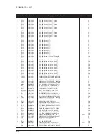
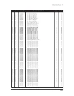
6 Electrical Parts List

6-17

Level

Loc. No.

Code No.

Description & Specification

Q'ty

SA/SNA

....4

C1074

2203-005005

C-CER,CHIP;100nF,10%,16V,X7R,1608

1

S.A

....4

C1078

2203-005005

C-CER,CHIP;100nF,10%,16V,X7R,1608

1

S.A

....4

C1079

2203-005005

C-CER,CHIP;100nF,10%,16V,X7R,1608

1

S.A

....4

C1093

2203-005005

C-CER,CHIP;100nF,10%,16V,X7R,1608

1

S.A

....4

C1104

2203-005005

C-CER,CHIP;100nF,10%,16V,X7R,1608

1

S.A

....4

C1148

2203-005005

C-CER,CHIP;100nF,10%,16V,X7R,1608

1

S.A

....4

C1169

2203-005005

C-CER,CHIP;100nF,10%,16V,X7R,1608

1

S.A

....4

C1181

2203-005005

C-CER,CHIP;100nF,10%,16V,X7R,1608

1

S.A

....4

C1194

2203-005005

C-CER,CHIP;100nF,10%,16V,X7R,1608

1

S.A

....4

C1207

2203-005005

C-CER,CHIP;100nF,10%,16V,X7R,1608

1

S.A

....4

C2042

2203-005005

C-CER,CHIP;100nF,10%,16V,X7R,1608

1

S.A

....4

C2045

2203-005005

C-CER,CHIP;100nF,10%,16V,X7R,1608

1

S.A

....4

C2047

2203-005005

C-CER,CHIP;100nF,10%,16V,X7R,1608

1

S.A

....4

C2049

2203-005005

C-CER,CHIP;100nF,10%,16V,X7R,1608

1

S.A

....4

C2055

2203-005005

C-CER,CHIP;100nF,10%,16V,X7R,1608

1

S.A

....4

C2060

2203-005005

C-CER,CHIP;100nF,10%,16V,X7R,1608

1

S.A

....4

C3009

2203-005005

C-CER,CHIP;100nF,10%,16V,X7R,1608

1

S.A

....4

C3010

2203-005005

C-CER,CHIP;100nF,10%,16V,X7R,1608

1

S.A

....4

C3014

2203-005005

C-CER,CHIP;100nF,10%,16V,X7R,1608

1

S.A

....4

C3015

2203-005005

C-CER,CHIP;100nF,10%,16V,X7R,1608

1

S.A

....4

C3016

2203-005005

C-CER,CHIP;100nF,10%,16V,X7R,1608

1

S.A

....4

C3018

2203-005005

C-CER,CHIP;100nF,10%,16V,X7R,1608

1

S.A

....4

C3019

2203-005005

C-CER,CHIP;100nF,10%,16V,X7R,1608

1

S.A

....4

C3022

2203-005005

C-CER,CHIP;100nF,10%,16V,X7R,1608

1

S.A

....4

C3026

2203-005005

C-CER,CHIP;100nF,10%,16V,X7R,1608

1

S.A

....4

C3027

2203-005005

C-CER,CHIP;100nF,10%,16V,X7R,1608

1

S.A

....4

C3032

2203-005005

C-CER,CHIP;100nF,10%,16V,X7R,1608

1

S.A

....4

C3037

2203-005005

C-CER,CHIP;100nF,10%,16V,X7R,1608

1

S.A

....4

C3040

2203-005005

C-CER,CHIP;100nF,10%,16V,X7R,1608

1

S.A

....4

C3042

2203-005005

C-CER,CHIP;100nF,10%,16V,X7R,1608

1

S.A

....4

C3044

2203-005005

C-CER,CHIP;100nF,10%,16V,X7R,1608

1

S.A

....4

C3046

2203-005005

C-CER,CHIP;100nF,10%,16V,X7R,1608

1

S.A

....4

C3047

2203-005005

C-CER,CHIP;100nF,10%,16V,X7R,1608

1

S.A

....4

C3049

2203-005005

C-CER,CHIP;100nF,10%,16V,X7R,1608

1

S.A

....4

C4002

2203-005005

C-CER,CHIP;100nF,10%,16V,X7R,1608

1

S.A

....4

C4097

2203-005005

C-CER,CHIP;100nF,10%,16V,X7R,1608

1

S.A

....4

C4101

2203-005005

C-CER,CHIP;100nF,10%,16V,X7R,1608

1

S.A

....4

C4103

2203-005005

C-CER,CHIP;100nF,10%,16V,X7R,1608

1

S.A

....4

C4107

2203-005005

C-CER,CHIP;100nF,10%,16V,X7R,1608

1

S.A

....4

C4112

2203-005005

C-CER,CHIP;100nF,10%,16V,X7R,1608

1

S.A

....4

C4115

2203-005005

C-CER,CHIP;100nF,10%,16V,X7R,1608

1

S.A

....4

C4131

2203-005005

C-CER,CHIP;100nF,10%,16V,X7R,1608

1

S.A

....4

C4133

2203-005005

C-CER,CHIP;100nF,10%,16V,X7R,1608

1

S.A

....4

C4135

2203-005005

C-CER,CHIP;100nF,10%,16V,X7R,1608

1

S.A

....4

C5001

2203-005005

C-CER,CHIP;100nF,10%,16V,X7R,1608

1

S.A

....4

C5002

2203-005005

C-CER,CHIP;100nF,10%,16V,X7R,1608

1

S.A

....4

C5011

2203-005005

C-CER,CHIP;100nF,10%,16V,X7R,1608

1

S.A

....4

C5012

2203-005005

C-CER,CHIP;100nF,10%,16V,X7R,1608

1

S.A

....4

C5084_LNA

2203-005005

C-CER,CHIP;100nF,10%,16V,X7R,1608

1

S.A

....4

C5085_RDY

2203-005005

C-CER,CHIP;100nF,10%,16V,X7R,1608

1

S.A

....4

C5115_RDY

2203-005005

C-CER,CHIP;100nF,10%,16V,X7R,1608

1

S.A

....4

C6000_FRC

2203-005005

C-CER,CHIP;100nF,10%,16V,X7R,1608

1

S.A

....4

C6001_FRC

2203-005005

C-CER,CHIP;100nF,10%,16V,X7R,1608

1

S.A

....4

C6002_FRC

2203-005005

C-CER,CHIP;100nF,10%,16V,X7R,1608

1

S.A

....4

C6003_FRC

2203-005005

C-CER,CHIP;100nF,10%,16V,X7R,1608

1

S.A

....4

C6004_FRC

2203-005005

C-CER,CHIP;100nF,10%,16V,X7R,1608

1

S.A

....4

C6005_FRC

2203-005005

C-CER,CHIP;100nF,10%,16V,X7R,1608

1

S.A

....4

C6006_FRC

2203-005005

C-CER,CHIP;100nF,10%,16V,X7R,1608

1

S.A

....4

C6007_FRC

2203-005005

C-CER,CHIP;100nF,10%,16V,X7R,1608

1

S.A

....4

C6008_FRC

2203-005005

C-CER,CHIP;100nF,10%,16V,X7R,1608

1

S.A

....4

C6011_FRC

2203-005005

C-CER,CHIP;100nF,10%,16V,X7R,1608

1

S.A

....4

C6012_FRC

2203-005005

C-CER,CHIP;100nF,10%,16V,X7R,1608

1

S.A

....4

C6013_FRC

2203-005005

C-CER,CHIP;100nF,10%,16V,X7R,1608

1

S.A

....4

C6014_FRC

2203-005005

C-CER,CHIP;100nF,10%,16V,X7R,1608

1

S.A

....4

C6015_FRC

2203-005005

C-CER,CHIP;100nF,10%,16V,X7R,1608

1

S.A

....4

C6016_FRC

2203-005005

C-CER,CHIP;100nF,10%,16V,X7R,1608

1

S.A

....4

C6023_FRC

2203-005005

C-CER,CHIP;100nF,10%,16V,X7R,1608

1

S.A

....4

C6024_FRC

2203-005005

C-CER,CHIP;100nF,10%,16V,X7R,1608

1

S.A

....4

C6025_FRC

2203-005005

C-CER,CHIP;100nF,10%,16V,X7R,1608

1

S.A

....4

C6026_FRC

2203-005005

C-CER,CHIP;100nF,10%,16V,X7R,1608

1

S.A

Summary of Contents for LE40M91B

Page 1: ...TFT LCD TV Chassis GMD40SEU Model LE40M91B Manual SERVICE TFT LCD TV Fashion Feature Luxurious Slim Design Supreme Picture Quality Supreme Sound Quality Supreme Convenience Quality Convenience for Users ...

Page 2: ...hout prior written permission of Samsung Electronics Co Ltd LE40M91BX Service Manual First edition June 2006 Printed in Korea Trademarks Samsung is the registered trademark of Samsung Electronics Co Ltd LE40M91BX and MacMaster Cable Adapter are trademarks of Samsung Electronics Co Ltd Macintosh Power Macintosh are trademarks of Apple Computer Inc All other trademarks are the property of their resp...

Page 3: ...Contents ...

Page 4: ...Contents ...

Page 5: ... City Gyeonggi Do Korea 443 742 Printed in Korea P N BN82 00145G 00 URL http itself sec samsung co kr This Service Manual is a property of Samsung Electronics Co Ltd Any unauthorized use of Manual can be punished under applicable International and or domestic law ...

Page 6: ...heck Figure 1 1 WARNING Do not use an isolation transformer during this test Use a leakage current tester or a metering system that complies with American National Standards Institute ANSI C101 1 Leakage Current for Appliances and Underwriters Laboratories UL Publication UL1410 59 7 Figure 1 1 Leakage Current Test Circuit 1 1 4 Product Safety Notices Some electrical and mechanical parts have speci...

Page 7: ...ord from the AC source and turn the power switch ON Connect an insulation resistance meter 500 V to the blades of the AC plug The insulation resistance between each blade of the AC plug and accessible conductive parts see above should be greater than 1 megohm 6 Always connect a test instrument s ground lead to the instrument chassis ground before connecting the positive lead always remove the inst...

Page 8: ...it may cause a fire or electric shock 5 Make sure to turn the power off and unplug the power cord from the outlet before repositioning the product Also check the antenna cable or the external connectors if they are fully unplugged Damage to the cord may cause fire or electric shock 6 Keep the antenna far away from any high voltage cables and install it firmly Contact with the high voltage cable or...

Page 9: ...hosting No Smearing Edge in image powered by Smooth Motion Driver Engine of Samsung LCD TV Wide Color Gamut More natural and vivid picture quality by WCG 127 High Dynamic Contrast 10000 1 Highest dynamic Contrast Ratio Best Off Angle Viewing Widened Viewing Angle 178 178 Left Right Real 10 Bit Panel 10 Bit Signal Processing 10 Bit Game Mode Present the most suitable picture for gaming Swivel Stand...

Page 10: ...8 mm AC power voltage Frequency AC 220 240V 50 60 Hz Power Consumption 210W 2W Dimensions W x D x H Set 994 x 326 x 696 mm 39 13 x 12 83 x 27 40 inches After installation Stand 994 x 92 x 647 mm 39 13 x 3 62 x 25 47 inches Without stand Weight Set After installation Stand 24 5Kg 54 01 lbs TV System Tunning Frequency Synthesize System PAL SECAM Sound MONO STEREO NICAM Environmental Considerations O...

Page 11: ... 30 61 kHz 60 75 Hz 16 777 216 colors PC Resolution Maximum mode Input Signal Sync Signal Video Signal Power Consumption Normal Power Saving 210W 2W 100W 125W 205W 1W H V Separate TTL P or N 0 7 Vp p 75ohm H V Separate TTL P or N 0 7 Vp p 75ohm WXGA 1360 x 768 60 Hz WXGA 1360 x 768 60 Hz LE26R71B LE32R71B LE40R71B 2 3 Spec Comparison ...

Page 12: ...Specifications 2 4 2 4 Option Specification Item Item Name Remote Control Batteries AAA x 2 Power Cord Cover Bottom Stand Cleaning Cloth BN59 00570A 3903 000042 BN63 02957A BN90 01048A BN63 01798A Code No Remark ...

Page 13: ...hing is essential 4 Avoid overload Excessive signal from a sweep generator might overload the front end of the TV When inserting signal markers do not allow the marker generator to distort test result 5 Connect the TV only to an AC power source with voltage and frequency as specified on the backcover nameplate 6 Do not attempt to connect or disconnect any wire while the TV is turned on Make sure t...

Page 14: ... 3 2 1 Entering Factory Mode If you have Factory remote control The buttons are active in the service mode 1 Remote Control Key Power Arrow Up Arrow Down Arrow Left Arrow Right Menu Enter Number Key 0 9 2 Function Control Key Power CH CH VOL VOL Menu TV VIDEO Enter ...

Page 15: ...Month Day Year Hour Min Sec 1 Calibration 1 AV Calibration 2 Comp Calibration 3 PC Calibration 4 HDMI Calibration 2 Option Table XXXX XXXX Inch Option Gamma Panel Option 2HDMI Hot Plug CLK C â Hot Plug Delay LNA 40 AMLCD LED_120 ON OFF ON OFF 9 ON ON OFF English ON OFF ON Flof OFF ON ON 8 Auto ON OFF Large OFF OFF SUWON UK OFF Carrier Mute Language Auto FM High Deviaion TTX TTX List ACR Dynamic CE...

Page 16: ... 32 129 128 129 128 128 128 128 32 128 128 128 140 129 128 128 28 130 128 120 TV AV Component PC DVI HDMI No 1 Item Motion Range 0 255 EEPROM TV AV S Video 80h Component PC Control IC Remark X No 1 2 3 4 5 Item V Peaking Peaking Delay Peaking Gain Peaking Width Peaking f0 Range 0 255 0 255 0 255 0 255 0 255 EEPROM TV AV 80h 80h 80h 80h 80h Component Control IC Remark X X X X X No 1 2 3 4 Range 0 2...

Page 17: ...20h 78h 78h 00h 40h 80h 80h D6h FEh FEh EEPROM Range TV AV S Video Component 00h 00h DVI HDMI PC 5 Picture Gain Adjust No Item 1 2 3 4 5 6 R Offset G Offset B Offset R Gain G Gain B Gain 00 255 00 255 00 255 00 255 00 255 00 255 151 SC1 RGB 151 SC1 RGB 151 SC1 RGB 123 SC1 RGB 123 SC1 RGB 123 SC1 RGB PC Calibration 128 PC Calibration 128 PC Calibration 128 PC Calibration 192 PC Calibration 192 PC C...

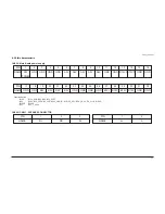
Page 18: ...6 17 No 1 2 3 4 5 Item Video Mute Time Melody Volume Ana_Dimm_Max TTX Contrast TTX Brightness Dynamic Contrast Dynamic Brightness Dynamic Color Dynamic Sharpness Standard Contrast Standard Brightness Standard Color Standard Sharpness Movie Contrast Movie Brightness Movie Color Movie Sharpness LNA PLUS RFDB_1 Level RFDB_2 Level RFDB_3 Level RFDB_4 Level 10 5 FEH 50 50 100 50 55 75 80 50 50 50 70 50...

Page 19: ...3 Alignments and Adjustments 3 7 1 2 3 4 Spectrum Delta Positive Negative ON 3 8 2 9 12C Check 10 Chip Debugger OFF 11 Checksum XXXX XXXX 12 Reset 13 Spread Spectrum ...

Page 20: ...nce Adjustment If picture color is wrong check White Balance condition Equipment CA210 Patten Toshiba Adjust W B in Factory Mode Sub brightness and R G B Offset controls low light region Sub contrast and R G B Gain controls high light region Source AV PAL composite Component 1280 720 60Hz HDMI DVI 1280 720 60Hz Toshiba Patten Test Pattern MSPG 945 Series Pattern 16 Color temperature 1500K 500 6 20...

Page 21: ...nput to the mode in which the adjustment will be made RF DTV PC DVI Input signal VIDEO Mode Model 2 744 484 Mode Pattern 16 DTV DVI Mode Model 6 1280 720 Mode Pattern 16 HDMI Mode Model 6 1280 720 Mode Pattern 16 b Enter factory color control confirm the data c Adjust the low light Refer to table 1 2 in adjustment position by mode Adjust sub Brightness to set the Y value Adjust red offset x and bl...

Page 22: ...ust the high light Refer to table 1 2 in adjustment position by mode Adjust red gain x and blue gain y to the color coordinates Do not adjust the green gain and sub contrast Y data Picture 4 3 Toshiba ABL Pattern High light Measurement point ...

Page 23: ...pgrade 3 5 1 How to Update Flash ROM 1 Installthe Flash Downloader ConnectSet Service Jack and Jig Cable to execute Program Update 2 Flash Downloader program update Before Turning on the set Click connect which is under of OSD Screen Turn on the Set ...

Page 24: ... burnt or damaged cable Check to see if there is a disconnected cable connection or a connection is too loose Check to see if the cables are connected according to the connection diagram 2 Check the power input to the Main Board 3 Check the voltage in and out between the SMPS Main Board between the SMPS INVERTER Board and between the Main LVDS Boards ...

Page 25: ... cable No Does proper DC A3 3V A5V appear at C1059 C1167 Check a IC1008 IC1004 Change a main PCB ass y Yes No Does proper DC 5V 3 3V 1 9V appear at C1015 C1194 C6026 Check a IC1015 IC812 IC1002 IC606 IC818 Change a main PCB ass y Yes A power is supplied to set Check a other function No picture part Replace a lcd panel No No LAMP off power indicator LED blue color ...

Page 26: ...ppear at the input of LBE RA6053 5 Check IC4001 Change a main PCB ass y Yes Yes No Yes Check a LVDS cable Replace a lcd panel Please Call to Samsung Co LTD No Does the digital data appear at the output of IC4003 RA6019_FRC 6021_FRC Check IC4003 Change a main PCB ass y No Does the digital data appear at the input of IC6003 6004 RA6001_FRC RA6003_FRC RA6005_FRC RA6009_FRC RA6016_FRC RA6018_FRC Check...

Page 27: ...4 Troubleshooting 4 4 WAVEFORMS 1 R G B Output Signal of IC500 ...

Page 28: ...s Power Indicator is off Lamp on no video No No No 3 2 Yes Check a LVDS cable Replace a lcd panel Please Call to Samsung Co LTD No Does the digital data appear at the output of IC4003 RA6019_FRC 6021_FRC Check IC4003 Change a main PCB ass y No Does the digital data appear at the input of IC6003 6004 RA6001_FRC RA6003_FRC RA6005_FRC RA6009_FRC RA6016_FRC RA6018_FRC Check IC6005 Change a main PCB as...

Page 29: ...4 Troubleshooting 4 6 2 Digital Output Data of IC500 3 Signal of HDMI Data ...

Page 30: ... on no picure No Connect the RF cable and check RF signal No No No Yes 4 4 3 Yes Check a LVDS cable Replace a lcd panel Please Call to Samsung Co LTD No Does the digital data appear at the output of IC4003 RA6019_FRC 6021_FRC Check IC4003 Change a main PCB ass y No Does the digital data appear at the input of IC6003 6004 RA6001_FRC RA6003_FRC RA6005_FRC RA6009_FRC RA6016_FRC RA6018_FRC Check IC600...

Page 31: ...4 Troubleshooting 4 8 WAVEFORMS 4 Tuner_CVBS Output Signal 3 CVBS Output Signal ...

Page 32: ... video signal No No Yes 4 Yes Check a LVDS cable Replace a lcd panel Please Call to Samsung Co LTD No Does the digital data appear at the output of IC4003 RA6019_FRC 6021_FRC Check IC4003 Change a main PCB ass y No Does the digital data appear at the input of IC6003 6004 RA6001_FRC RA6003_FRC RA6005_FRC RA6009_FRC RA6016_FRC RA6018_FRC Check IC6005 Change a main PCB ass y Yes Does the digital data...

Page 33: ...4 Troubleshooting 4 10 WAVEFORMS 4 CVBS Output Signal ...

Page 34: ...a IC4001 Change a main PCB ass y No Yes 5 2 Yes Check a LVDS cable Replace a lcd panel Please Call to Samsung Co LTD No Does the digital data appear at the output of IC4003 RA6019_FRC 6021_FRC Check IC4003 Change a main PCB ass y No Does the digital data appear at the input of IC6003 6004 RA6001_FRC RA6003_FRC RA6005_FRC RA6009_FRC RA6016_FRC RA6018_FRC Check IC6005 Change a main PCB ass y Yes Doe...

Page 35: ...4 Troubleshooting 4 12 2 Digital Output Data of IC500 5 Analog Signal Y C to IC500 WAVEFORMS ...

Page 36: ...nection harness and headphone jack Side AV Yes Yes No Check the DC 12V of IC1015 Check a IC1015 Change a main PCB ass y Yes No Does the signal appear at L1014 L1015 L1018 L1019 Change a main PCB ass y Yes Replace the speaker ass y No 4 2 7 No Sound 6 7 Connect a sound cable control a volume Picture is display no sound No ...

Page 37: ...4 Troubleshooting 4 14 WAVEFORMS 6 The Signal are Inputed to IC1015 7 DC 12V ...

Page 38: ...Exploded View Parts List 5 1 5 Exploded View and Parts List You can search for updated part codes through ITSELF web site URL http itself sec samsung co kr T0003 T0175 T0175 M0215 T0447 M0014 M0013 M0013 ...

Page 39: ... T0175 BN96 03271A ASSY SPEAKER P 8ohm Mosel 32 Left 10W BA 1 S A T0175 BN96 03272A ASSY SPEAKER P 8ohm Mosel 32 Right 10W B 1 S A M0215 BN07 00343A LCD PANEL LTA400WH LL1 10bit 40inch 1 07 1 S A T0447 BN96 04218A ASSY BRACKET P PANEL 40M9 EO LED MOSEL 1 S N A M0014 BN94 01065A ASSY PCB MAIN LE40M91BX XEC 1 S A M0013 BN96 04217A ASSY STAND P BASE LED MOSEL 40 ABS PMMA 1 S A ...

Page 40: ...04216A ASSY COVER P 40M9 EO HIPS HB BK500 1 S A 3 M0081 6003 001003 SCREW TAPTITE BH B M4 L12 ZPC BLK SWR 2 S N A 3 T0069 AA63 60122K SPACER FELT SPD 42P3S FELT L60 D20 T0 35 7 S N A 3 M0006 BN63 02830A COVER REAR 40 LED MOSEL HIPS HB BK500 1 S N A 3 T0071 BN64 00481A INLAY TERMINAL MOSEL 40 EO PS SHEET T0 5 1 S N A 3 T0064 BN65 00002A CLAMPER CORE BORDEAUX PP V0 BLK 1 S N A 3 BN61 02776A HOLDER W...

Page 41: ...WITCHING MMBD4148SE 100V 200mA SO 1 S A 4 D2068 0401 001056 DIODE SWITCHING MMBD4148SE 100V 200mA SO 1 S A 4 D2069 0401 001056 DIODE SWITCHING MMBD4148SE 100V 200mA SO 1 S A 4 D2072 0401 001056 DIODE SWITCHING MMBD4148SE 100V 200mA SO 1 S A 4 D2085 0401 001056 DIODE SWITCHING MMBD4148SE 100V 200mA SO 1 S A 4 D2086 0401 001056 DIODE SWITCHING MMBD4148SE 100V 200mA SO 1 S A 4 D2087 0401 001056 DIODE...

Page 42: ...0406 001172 DIODE TVS CDS3C30GTH 48V 0W SMD 1 S A 4 D2082 0406 001172 DIODE TVS CDS3C30GTH 48V 0W SMD 1 S A 4 D2083 0406 001172 DIODE TVS CDS3C30GTH 48V 0W SMD 1 S A 4 D1002 0407 000123 DIODE ARRAY DAN202K 80V 100mA CA2 3 SOT 1 S A 4 D1011 0407 000123 DIODE ARRAY DAN202K 80V 100mA CA2 3 SOT 1 S A 4 D1020 0407 000123 DIODE ARRAY DAN202K 80V 100mA CA2 3 SOT 1 S A 4 D3001 0407 000123 DIODE ARRAY DAN2...

Page 43: ...OSI FIXED REG AP1117D 25A TO 252 3P 1 S A 4 IC012 1203 003000 IC POSI ADJUST REG MIC49150WR S PAK 5P 1 S A 4 IC012 1203 003038 IC POSI ADJUST REG LP2995 SO 8P 4 9x3 9 1 S A 4 T0170 1203 003059 IC SWITCH VOL REG MP1583 SOIC 8P 4 9x3 1 S A 4 T0170 1203 003059 IC SWITCH VOL REG MP1583 SOIC 8P 4 9x3 1 S A 4 T0087 1203 003561 IC POSI FIXED REG NCP551SN15T1G TSOP 5 1 S A 4 IC1009 1204 002464 IC AUDIO PR...

Page 44: ...07 000070 R CHIP 0ohm 5 1 10W TP 1608 1 S A 4 R2112 2007 000070 R CHIP 0ohm 5 1 10W TP 1608 1 S A 4 R2113 2007 000070 R CHIP 0ohm 5 1 10W TP 1608 1 S A 4 R2114 2007 000070 R CHIP 0ohm 5 1 10W TP 1608 1 S A 4 R2115 2007 000070 R CHIP 0ohm 5 1 10W TP 1608 1 S A 4 R2233 2007 000070 R CHIP 0ohm 5 1 10W TP 1608 1 S A 4 R3003 2007 000070 R CHIP 0ohm 5 1 10W TP 1608 1 S A 4 R3024 2007 000070 R CHIP 0ohm ...

Page 45: ...07 000071 R CHIP 22ohm 5 1 10W TP 1608 1 S A 4 R2246 2007 000071 R CHIP 22ohm 5 1 10W TP 1608 1 S A 4 R2247 2007 000071 R CHIP 22ohm 5 1 10W TP 1608 1 S A 4 R2251 2007 000071 R CHIP 22ohm 5 1 10W TP 1608 1 S A 4 R2252 2007 000071 R CHIP 22ohm 5 1 10W TP 1608 1 S A 4 R2253 2007 000071 R CHIP 22ohm 5 1 10W TP 1608 1 S A 4 R2254 2007 000071 R CHIP 22ohm 5 1 10W TP 1608 1 S A 4 R4015 2007 000071 R CHI...

Page 46: ...011 2007 000074 R CHIP 100ohm 5 1 10W TP 1608 1 S A 4 R1012 2007 000074 R CHIP 100ohm 5 1 10W TP 1608 1 S A 4 R1013 2007 000074 R CHIP 100ohm 5 1 10W TP 1608 1 S A 4 R1014 2007 000074 R CHIP 100ohm 5 1 10W TP 1608 1 S A 4 R1017 2007 000074 R CHIP 100ohm 5 1 10W TP 1608 1 S A 4 R1018 2007 000074 R CHIP 100ohm 5 1 10W TP 1608 1 S A 4 R1032 2007 000074 R CHIP 100ohm 5 1 10W TP 1608 1 S A 4 R1033 2007...

Page 47: ...00077 R CHIP 470ohm 5 1 10W TP 1608 1 S A 4 R1054 2007 000077 R CHIP 470ohm 5 1 10W TP 1608 1 S A 4 R1098 2007 000077 R CHIP 470ohm 5 1 10W TP 1608 1 S A 4 R2004 2007 000077 R CHIP 470ohm 5 1 10W TP 1608 1 S A 4 R2006 2007 000077 R CHIP 470ohm 5 1 10W TP 1608 1 S A 4 R2033 2007 000077 R CHIP 470ohm 5 1 10W TP 1608 1 S A 4 R2034 2007 000077 R CHIP 470ohm 5 1 10W TP 1608 1 S A 4 R2037 2007 000077 R ...

Page 48: ... 10W TP 1608 1 S A 4 R3082 2007 000084 R CHIP 4 7Kohm 5 1 10W TP 1608 1 S A 4 R3086 2007 000084 R CHIP 4 7Kohm 5 1 10W TP 1608 1 S A 4 R3087 2007 000084 R CHIP 4 7Kohm 5 1 10W TP 1608 1 S A 4 R3108 2007 000084 R CHIP 4 7Kohm 5 1 10W TP 1608 1 S A 4 R3109 2007 000084 R CHIP 4 7Kohm 5 1 10W TP 1608 1 S A 4 R3110 2007 000084 R CHIP 4 7Kohm 5 1 10W TP 1608 1 S A 4 R3111 2007 000084 R CHIP 4 7Kohm 5 1 ...

Page 49: ...7 000093 R CHIP 20Kohm 5 1 10W TP 1608 1 S A 4 R2161 2007 000093 R CHIP 20Kohm 5 1 10W TP 1608 1 S A 4 R3004 2007 000094 R CHIP 22Kohm 5 1 10W TP 1608 1 S A 4 R5154_RDY 2007 000094 R CHIP 22Kohm 5 1 10W TP 1608 1 S A 4 R2010 2007 000097 R CHIP 47Kohm 5 1 10W TP 1608 1 S A 4 R2011_EU 2007 000097 R CHIP 47Kohm 5 1 10W TP 1608 1 S A 4 R2012_EU 2007 000097 R CHIP 47Kohm 5 1 10W TP 1608 1 S A 4 R2162 2...

Page 50: ...7 000309 R CHIP 10ohm 5 1 10W TP 1608 1 S A 4 R3067 2007 000309 R CHIP 10ohm 5 1 10W TP 1608 1 S A 4 R3068 2007 000309 R CHIP 10ohm 5 1 10W TP 1608 1 S A 4 R3069 2007 000309 R CHIP 10ohm 5 1 10W TP 1608 1 S A 4 R3091 2007 000309 R CHIP 10ohm 5 1 10W TP 1608 1 S A 4 R3092 2007 000309 R CHIP 10ohm 5 1 10W TP 1608 1 S A 4 R3093 2007 000309 R CHIP 10ohm 5 1 10W TP 1608 1 S A 4 R3094 2007 000309 R CHIP...

Page 51: ...4 R2175_EU 2007 007733 R CHIP 51ohm 1 1 10W TP 1608 1 S A 4 R1083 2007 008720 R CHIP 4 7ohm 1 1 4W TP 3216 1 S A 4 R1088 2007 008720 R CHIP 4 7ohm 1 1 4W TP 3216 1 S A 4 R1094 2007 008720 R CHIP 4 7ohm 1 1 4W TP 3216 1 S A 4 R1097 2007 008720 R CHIP 4 7ohm 1 1 4W TP 3216 1 S A 4 RA4005_FRC 2011 000002 R NET 22ohm 5 1 16W L CHIP 8P TP 3216 1 S A 4 RA4006_FRC 2011 000002 R NET 22ohm 5 1 16W L CHIP 8...

Page 52: ...IP 8P TP 3216 1 S A 4 RA3006 2011 001093 R NET 100OHM 5 1 16W L CHIP 8P TP 3216 1 S A 4 RA3010 2011 001093 R NET 100OHM 5 1 16W L CHIP 8P TP 3216 1 S A 4 RA3012 2011 001093 R NET 100OHM 5 1 16W L CHIP 8P TP 3216 1 S A 4 RA3013 2011 001093 R NET 100OHM 5 1 16W L CHIP 8P TP 3216 1 S A 4 RA3014 2011 001093 R NET 100OHM 5 1 16W L CHIP 8P TP 3216 1 S A 4 RA3015 2011 001093 R NET 100OHM 5 1 16W L CHIP 8...

Page 53: ...0 25V Y5V 1608 1 S A 4 C4036 2203 000189 C CER CHIP 100nF 80 20 25V Y5V 1608 1 S A 4 C4038 2203 000189 C CER CHIP 100nF 80 20 25V Y5V 1608 1 S A 4 C4039 2203 000189 C CER CHIP 100nF 80 20 25V Y5V 1608 1 S A 4 C4040 2203 000189 C CER CHIP 100nF 80 20 25V Y5V 1608 1 S A 4 C4041 2203 000189 C CER CHIP 100nF 80 20 25V Y5V 1608 1 S A 4 C4042 2203 000189 C CER CHIP 100nF 80 20 25V Y5V 1608 1 S A 4 C4043...

Page 54: ...10nF 10 50V X7R 1608 1 S A 4 C1198 2203 000257 C CER CHIP 10nF 10 50V X7R 1608 1 S A 4 C2056 2203 000257 C CER CHIP 10nF 10 50V X7R 1608 1 S A 4 C2065 2203 000257 C CER CHIP 10nF 10 50V X7R 1608 1 S A 4 C2066 2203 000257 C CER CHIP 10nF 10 50V X7R 1608 1 S A 4 C2068 2203 000257 C CER CHIP 10nF 10 50V X7R 1608 1 S A 4 C3035 2203 000257 C CER CHIP 10nF 10 50V X7R 1608 1 S A 4 C4005 2203 000257 C CER...

Page 55: ...30 2203 000815 C CER CHIP 0 033nF 5 50V C0G 1608 1 S A 4 C2031 2203 000815 C CER CHIP 0 033nF 5 50V C0G 1608 1 S A 4 C1119 2203 000888 C CER CHIP 4 7nF 10 50V X7R 1608 1 S A 4 C1120 2203 000888 C CER CHIP 4 7nF 10 50V X7R 1608 1 S A 4 C4003 2203 000888 C CER CHIP 4 7nF 10 50V X7R 1608 1 S A 4 C4004 2203 000888 C CER CHIP 4 7nF 10 50V X7R 1608 1 S A 4 C5003 2203 000888 C CER CHIP 4 7nF 10 50V X7R 1...

Page 56: ...05 C CER CHIP 100nF 10 16V X7R 1608 1 S A 4 C4002 2203 005005 C CER CHIP 100nF 10 16V X7R 1608 1 S A 4 C4097 2203 005005 C CER CHIP 100nF 10 16V X7R 1608 1 S A 4 C4101 2203 005005 C CER CHIP 100nF 10 16V X7R 1608 1 S A 4 C4103 2203 005005 C CER CHIP 100nF 10 16V X7R 1608 1 S A 4 C4107 2203 005005 C CER CHIP 100nF 10 16V X7R 1608 1 S A 4 C4112 2203 005005 C CER CHIP 100nF 10 16V X7R 1608 1 S A 4 C4...

Page 57: ...0 20 10V Y5V 1608 1 S A 4 C4106 2203 005065 C CER CHIP 1000nF 80 20 10V Y5V 1608 1 S A 4 C4113 2203 005065 C CER CHIP 1000nF 80 20 10V Y5V 1608 1 S A 4 C4114 2203 005065 C CER CHIP 1000nF 80 20 10V Y5V 1608 1 S A 4 C4117 2203 005065 C CER CHIP 1000nF 80 20 10V Y5V 1608 1 S A 4 C4118 2203 005065 C CER CHIP 1000nF 80 20 10V Y5V 1608 1 S A 4 C6055_FRC 2203 005065 C CER CHIP 1000nF 80 20 10V Y5V 1608 ...

Page 58: ...5R TP 3216 1 S A 4 C1083 2203 006333 C CER CHIP 10000nF 20 16V X5R TP 3216 1 S A 4 C1085 2203 006333 C CER CHIP 10000nF 20 16V X5R TP 3216 1 S A 4 C1088 2203 006333 C CER CHIP 10000nF 20 16V X5R TP 3216 1 S A 4 C1089 2203 006333 C CER CHIP 10000nF 20 16V X5R TP 3216 1 S A 4 C1090 2203 006333 C CER CHIP 10000nF 20 16V X5R TP 3216 1 S A 4 C1091 2203 006333 C CER CHIP 10000nF 20 16V X5R TP 3216 1 S A...

Page 59: ...32 2402 001097 C AL SMD 0 1UF 20 50V WT TP 4 3X4 3X5 2 1 S A 4 C5033 2402 001097 C AL SMD 0 1UF 20 50V WT TP 4 3X4 3X5 2 1 S A 4 C1010 2402 001128 C AL SMD 100 ìF 20 16V TP 6 3X5 7mm 1 S A 4 C1015 2402 001128 C AL SMD 100 ìF 20 16V TP 6 3X5 7mm 1 S A 4 C1036 2402 001128 C AL SMD 100 ìF 20 16V TP 6 3X5 7mm 1 S A 4 C1042 2402 001128 C AL SMD 100 ìF 20 16V TP 6 3X5 7mm 1 S A 4 C1059 2402 001128 C AL ...

Page 60: ...1 2801 003954 CRYSTAL SMD 27MHz 30ppm 28 AAN 16pF 50oh 1 S A 4 X6000_FRC 2801 004004 CRYSTAL SMD 20 25MHz 20ppm 28 AAN 13pF 2 1 S A 4 X4001 2801 004483 CRYSTAL SMD 28 322MHz 30ppm HC 49 20pF 5 1 S A 4 F103 2901 001114 FILTER EMI SMD 25VDC 2 0ADC 100nF 3 2x 1 S A 4 T0568 3301 000314 BEAD SMD 120ohm 1 6x0 8x0 8mm 1 S N A 4 T0568 3301 000314 BEAD SMD 120ohm 1 6x0 8x0 8mm 1 S N A 4 T0568 3301 001145 B...

Page 61: ... 200ohm 2 0x1 2x1 3mm 150mA TP 1 S N A 4 T0568 3301 001593 BEAD SMD 200ohm 2 0x1 2x1 3mm 150mA TP 1 S N A 4 T0568 3301 001593 BEAD SMD 200ohm 2 0x1 2x1 3mm 150mA TP 1 S N A 4 CN2001 3701 001311 CONNECTOR HDMI 21P 2R FEMALE SMD S AU30U 1 S A 4 CN2003 3701 001311 CONNECTOR HDMI 21P 2R FEMALE SMD S AU30U 1 S A 4 CN330 3711 005291 HEADER BOARD TO CABLE BOX 2P 1R 2MM SMD 1 S A 4 CN330 3711 005292 HEADE...

Page 62: ...1117D 25A TO 252 3P 1 S A 4 IC1 1204 002585 IC DECODER MP612 LFBGA 256P 17x17mm PLAS 1 S A 4 IC2 1205 002713 IC CODEC ALC202A LQFP 48P 7X7MM PLASTIC 1 S A 4 R11 2007 000043 R CHIP 1Kohm 1 1 10W TP 1608 1 S A 4 R12 2007 000043 R CHIP 1Kohm 1 1 10W TP 1608 1 S A 4 R120 2007 000070 R CHIP 0ohm 5 1 10W TP 1608 1 S A 4 R138 2007 000070 R CHIP 0ohm 5 1 10W TP 1608 1 S A 4 R148 2007 000070 R CHIP 0ohm 5 ...

Page 63: ...7 000090 R CHIP 10Kohm 5 1 10W TP 1608 1 S A 4 R82 2007 000090 R CHIP 10Kohm 5 1 10W TP 1608 1 S A 4 R83 2007 000090 R CHIP 10Kohm 5 1 10W TP 1608 1 S A 4 R84 2007 000090 R CHIP 10Kohm 5 1 10W TP 1608 1 S A 4 R85 2007 000090 R CHIP 10Kohm 5 1 10W TP 1608 1 S A 4 R86 2007 000090 R CHIP 10Kohm 5 1 10W TP 1608 1 S A 4 R87 2007 000090 R CHIP 10Kohm 5 1 10W TP 1608 1 S A 4 R88 2007 000090 R CHIP 10Kohm...

Page 64: ...nF 10 16V X7R 1608 1 S A 4 C136 2203 005005 C CER CHIP 100nF 10 16V X7R 1608 1 S A 4 C137 2203 005005 C CER CHIP 100nF 10 16V X7R 1608 1 S A 4 C138 2203 005005 C CER CHIP 100nF 10 16V X7R 1608 1 S A 4 C139 2203 005005 C CER CHIP 100nF 10 16V X7R 1608 1 S A 4 C140 2203 005005 C CER CHIP 100nF 10 16V X7R 1608 1 S A 4 C141 2203 005005 C CER CHIP 100nF 10 16V X7R 1608 1 S A 4 C142 2203 005005 C CER CH...

Page 65: ...03 005065 C CER CHIP 1000nF 80 20 10V Y5V 1608 1 S A 4 C110 2203 005065 C CER CHIP 1000nF 80 20 10V Y5V 1608 1 S A 4 C111 2203 005065 C CER CHIP 1000nF 80 20 10V Y5V 1608 1 S A 4 C112 2203 005065 C CER CHIP 1000nF 80 20 10V Y5V 1608 1 S A 4 C113 2203 005065 C CER CHIP 1000nF 80 20 10V Y5V 1608 1 S A 4 C10 2203 006333 C CER CHIP 10000nF 20 16V X5R TP 3216 1 S A 4 C11 2203 006333 C CER CHIP 10000nF ...

Page 66: ...CRYSTAL SMD 13 5MHz 30ppm 28 AAN 20 40oh 1 S A 4 CN3 3709 001290 CONNECTOR CARD SLOT 50P 1 27MM SMD A AU1 1 S A 4 CN8 3709 001424 CONNECTOR CARD SLOT 70pin 0 6 gold car 1 S A 4 CN4 3722 002236 JACK MINI USB 5P AU30U BLK SMD A MINI US 1 S A 4 T0077 BN41 00746B PCB MAIN MOSEL FR 4 6 1 0 1 6T 179 184 3 1 S N A 4 M0018 BN97 01024A ASSY MICOM 29LV320 T MSLMPEUW 1008 2006 1 S A 5 IC115 1107 001475 IC FL...

Page 67: ... Conductive Fabric 0 1 S N A 2 CIS BN63 02996A GASKET TAPE MOSELLED Conductive Fabric 0 1 S N A 2 T0890 BN96 04468A ASSY FAN P 2 BALL BEARINGS 61 6X60X15 0 1 S N A 0 1 M0019 BN92 01981W ASSY LABEL LE40M91BX 1 S N A 0 1 M0003 BN92 01986U ASSY BOX 40M91 XEE 1 S N A 2 BN69 01498A BOX INNER LED40 MOSEL DY 04 AB YEL C 01 1 02 S N A 2 M0006 BN69 01499A BOX 00 SET OUT 40M9 CB DY 06 AB YEL C3 H 1 02 S N A...

Page 68: ...7 Block Diagrams 7 1 7 Block Diagram This Document can not be used without Samsung s authorization ...

Page 69: ...8 1 8 Wiring Diagrams 8 Wiring Diagram 8 1 LE40M91BX Wiring Diagram ...

Page 70: ...8 Wiring Diagrams 8 2 8 2 Main Board Layout ...

Page 71: ... B12VSB12VS GND GND POWER PIN 17 18 19 20 21 22 23 24 25 26 27 28 29 30 31 32 NAME GND GND B5V B5V B5V B5V GND GND GND GND B12V B12V B12V B12V GND GND Function Define B12V B12V_CHN B9V B8V B5V_VCCT B5V B33V B5V_VCCA B3 3VD B2 5V_VDD B1 8VD PX_VD1 8 PX_VA1 8 PX_VL1 8 B1 2VD B12VS B12VS A5V A5V_1 A3 3V CN600 CN601 SPEAKER CONNECTOR PIN 1 2 3 NAME R NC R PIN 1 2 NAME L L ...

Page 72: ... A5V Front control board poewr supply KEY INPUT1 2 Key control from the memu change up down Etc IR Remote control signal LED Control the timing and stand by LED color CN501 Panel control PIN 1 2 3 4 5 NAME SW_inverter Ana_dimming PWM_dimming GND Sensor_Power Function Define SW_inverter panel inverter control about 3 3V Ana_dimming panel dimming control PWM_dimming panel PWM control duty 40 90 ...

Page 73: ...27 TXOUTO1 6 GND 28 TXOUTO1 7 GND 29 TXOUTO2 8 GND 30 TXOUTO2 9 GND 31 GND 10 TXOUTO0 32 TXOUTOC 11 TXOUTO0 33 TXOUTOC 12 TXOUTO1 34 GND 13 TXOUTO1 35 TXOUTO3 14 TXOUTO2 36 TXOUTO3 15 TXOUTO2 37 TXOUTO4 16 GND 38 TXOUTO4 17 TXOUTOC 39 GND 18 TXOUTOC 40 CTRL1 19 GND 41 CTRL2 20 TXOUTO3 42 CTRL3 21 TXOUTO3 43 LVDS OPTION 22 TXOUTO4 44 DOC OPTION ...

Page 74: ...8 Wiring Diagrams 8 6 8 4 Power Board Layout ...

Page 75: ... 1 2 3 4 5 6 7 8 9 10 11 12 13 14 15 16 NAME 13V GND 5 4V 5 4V 5 4V GND GND GND 12V 12V 12V GND GND GND ST7V PWR Functing Define ST7V Stand By Output PWR Power On Off Control Refer to CN801 function define CNM804 Panel control PIN 1 2 3 4 5 NAME SW_inverter Ana_dimming PWM_dimming GND SENSOR POWER Functing Define Refer to CN815 function define ...

Page 76: ...AMLCD Panel Inverter Power 24V LAMP INVERTER Voltage B L Brightness sensor power A_D ANA_DIMMING P_D PWM_DIMMING CN803 Inverter power supply PIN 1 2 3 4 5 6 7 8 9 10 11 12 13 14 NAME 24V 24V 24V 24V 24V GND GND GND GND GND A_D B L P_D GND Functing Define AUO Panel Inverter Power 24V LAMP INVERTER Voltage B L Brightness sensor power A_D ANA_DIMMING P_D PWM_DIMMING ...

Page 77: ...8 9 8 Wiring Diagrams ...

Page 78: ...N 1 2 3 4 5 6 7 8 9 10 11 12 13 14 15 16 NAME 13V GND 5 4V 5 4V 5 4V GND GND GND 12V 12V 12V GND GND GND ST7V PWR Functing Define ST7V Stand By Output PWR Power On Off Control Refer to CN801 function define CNM804 Panel control PIN 1 2 3 4 5 NAME SW_inverter Ana_dimming PWM_dimming GND SENSOR POWER Functing Define Refer to CN815 function define ...

Page 79: ...g Define AMLCD Panel Inverter Power 24V LAMP INVERTER Voltage B L Brightness sensor power A_D ANA_DIMMING P_D PWM_DIMMING CN804 Inverter power supply PIN 1 2 3 4 5 6 7 8 9 10 11 12 13 14 NAME 24V 24V 24V 24V 24V GND GND GND GND GND B D P_L GND B L Functing Define CMO Panel Inverter Power 24V LAMP INVERTER Voltage B L Brightness sensor power P_D PWM_DIMMING ...

Page 80: ...195_NT 50V 15Kohm R 1066 120uF C1095 R 1116 100ohm 6 3V 10Kohm R 1067 C1145 100nF C1136 10uF B3 3VD B5V 16V C1007 47uF 100pF C1162 68K ohm R 1022 L1018 100ohm R 1012 C1204 100uF 25V R 1004 C1070 22pF 100ohm 68K ohm R 1035 R 1009 C1043 100nF 4 7Kohm C1089 10uF R LZ3 3A TE 11 D1021 16V C1115 220nF C1056 R 1121 100ohm S OUND_AMP 100uF 100nF C1055 L1009 22uH 10V 1mF C1102 C1187 10uF 10uF C1205 R 1014 ...

Page 81: ...9 Schematic Diagrams 9 2 9 2 Input Output Schematic Diagram ...

Page 82: ...9 Schematic Diagrams 9 3 9 3 Input Output Schematic Diagram ...

Page 83: ...9 Schematic Diagrams 9 4 9 4 Micom Schematic Diagram ...

Page 84: ...9 Schematic Diagrams 9 5 9 5 SVP PX Schematic Diagram ...

Page 85: ...9 Schematic Diagrams 9 6 9 6 Application Schematic Diagram ...

Page 86: ...9 Schematic Diagrams 9 7 9 7 FRCH 100Hz LVDS Schematic Diagram ...

Page 87: ...9 Schematic Diagrams 9 8 Memo ...

Page 88: ...ncrease the volume In the on screen menu use the buttons as you use the and buttons on the remote control 4 C P Press to change channels In the on screen menu use the C P buttons as you use the and buttons on the remote control Without the Remote Control you can turn on the TV by using the Channel buttons 5 Speakers 6 POWER Press to turn the TV on and off Power Indicator Blinks and turns off when ...

Page 89: ...ating Instructions and Installation 10 2 Whenever you connect an external device to your TV make sure that power on the unit is turned off When connecting an external device match the colour of the connection terminal to the cable ...

Page 90: ...o an appropriate external A V device such as VCR DVD or Camcorder Connect RCA audio cables to R AUDIO L on the rear of your set and the other ends to corresponding audio out connectors on the A V device Headphone may be connected to the headphone output 4 on the rear of your set While the headphone is connected the sound from the built in speakers will be disabled 6 SERVICE Service connection for ...

Page 91: ...T Adjusts 5 separate devices TV DVD STB CABLE or VCR RESET When your remote does not work change the batteries and press the RESET button for 2 3 seconds before use 18 Available source selection 19 When pressing this button a number of buttons on the remote control e g Selects a target device volume channel and MUTE buttons light up for a few seconds and then turn off to save power This function i...

Page 92: ...e 10 5 Installing the Wall Mount Kit Wall mount items sold separately allow you to mount the TV on the wall For detailed information on installing the wall mount see the instructions provided with the Wall Mount items Contact a technician for assistance when installing the wall mounted bracket Samsung Electronics is not responsible for any damage to the product or injury to yourself or others if y...

Page 93: ...or contains electrostatically sensitive devices Use caution when handling these components 11 1 Disassembly Cautions 1 Disconnect the monitor from the power source before disassembly 2 Follow these directions carefully never use metal instruments to pry apart the cabinet Description Picture Description 1 Place monitor face down on cushioned table Remove screws from the Stand Remove stand ...

Page 94: ...ssembly and Reassembly 11 2 3 Disconnet cables from the main and power boards Remove screws from the side AV jack Description Picture Description 2 Remove screws from the rear cover and lift up the rear cover ...

Page 95: ...11 Disassembly and Reassembly 11 3 5 Lift up the speakers Remove screws from the BRKT Description Picture Description 4 Remove screws from the boards and stand BRKT ...

Page 96: ...11 Disassembly and Reassembly 11 4 7 Lift up the panel BRKT Description Picture Description 6 Lift up the Panel and remove screws ...

Page 97: ...11 Disassembly and Reassembly 11 5 11 2 Reassembly Reassembly procedures are in the reverse order of disassembly procedures ...

Page 98: ...12 PCB Diagram 12 1 12 PCB Diagram 12 1 Main PCB Layout ...

Page 99: ...12 PCB Diagram 12 2 12 2 SMPS PCB Layout ...
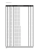
Page 100: ...ription Mosel consists of three main blocks 1 Main board Video signal processing 2 IP board Power supply Inverter 3 T con board LCD Panel control MMS RF In Air Cable Scart 1 2 A V S Video Component PC HDMI1 2 Main Board Panel T con Board Speaker IR LED Signal Power SMPS ...

Page 101: ... of three main blocks 1 Main board Video signal processing 2 SMPS Power supply 3 T con board LCD Panel control SMPS INVERTER Main Board Panel T con Board Speaker IR LED Signal Power RF In Air Cable Scart 1 2 A V S Video Component MMS PC HDMI1 2 ...

Page 102: ...onvert various input resolution to other resolution ex 640 480 to 1024 768 Auto Configuration Auto adjustment This is an algorithm to adjust monitor to optimum condition by pushing one key OSD On Screen Display On screen display customer can control the screen easily with this Image Lock This means Fineness adjustment in LCD Monitor the features are Fine and Coarse FINE Fine adjustment is used to ...

Page 103: ...kHz Interlace and Non Interlace Methods Showing the horizontal lines of the screen from the top to the bottom in order is called the Non Interlace method while showing odd lines and then even lines in turn is called the Interlace method The Non Interlace method is used for the majority of monitors to ensure a clear image The Interlace method is the same as that used in TVs Plug Play This is a func...

Page 104: ...m VHF or UHF broadcasting by terrestrial broadcasters The CATV programs may include movies entertain ment and educational programs Different from cable TV CATV can be viewed only within the area in which the CATV service is offered S Video Short for Super Video S Video allows up to 800 lines of horizontal resolution enabling high quality video VHF UHF VHF indicates TV channels 2 to 13 and UHF indi...

Page 105: ... Assignments NC DDC Input power 5V IDENT DVI Output Signal HDCP Control Rx0 Rx0 GND NC NC GND RxC RxC 13 14 15 16 17 18 19 20 21 22 23 24 1 2 3 4 5 6 7 8 9 10 11 12 Rx2 Rx2 GND NC NC DDC SCL DDC SDA NC Rx1 Rx1 GND NC Sync Type Pin No 24P DVI D Figure 1 ...

Page 106: ...2 3 4 5 6 7 8 9 10 11 12 13 14 15 Red Green Blue GND GND GND Red GND Green GND Blue DDC Input power 5V IDENT PC GND DDC Data SDA H SYNC V SYNC DDC Clock SCL 14 2 5 D SUB 14 2 2 Component RCA White RCA Red CVBS Audio L GND Audio R GND 14 2 4 A V RCA Yellow 14 2 6 PC Display mode Mode Resolution Horizontal Frequency kHz 640 x 480 720 x 400 640 x 480 640 x 480 800 x 600 800 x 600 800 x 600 1024 x 768...

Page 107: ...d input 16 Fast Blanking signal RGB switching 17 Video output GND 18 Video input GND 19 Video output CVBS out 20 Video input CVBS in 21 Common GND Pin Signal 1 Audio output R 2 Audio input R 3 Audio output L 4 Audio common GND 5 Video GND RGB blue 6 Audio input L 7 RGB blue input 8 Switching voltage 9 Video GND RGB green 10 NC 11 RGB green input Pin Signal 12 NC 13 Video GND RGB red 14 GND 15 RGB ...

Page 108: ...er L R Data time Front porch Sync width Back porch Sync polarity VERTICAL Frequency Total time Active time Blank time Border L R Data time Front porch Sync width Back porch Sync polarity Dot Clock Border R or B Pulse Width Front Porch Back Porch Border L or T Blank Time Data Time Active Time 85 500MHz Sync Type Scan Type Separate N I 47 712kHz 20 959 15 906 5 053 0 000 15 906 0 749 1 702 2 994 Pos...

Page 109: ... N I 31 469kHz 31 778 26 058 5 720 0 318 25 422 0 318 3 813 1 589 Negative IBM VGA3 640 x 480 3 59 940kHz 16 683ms 15 761ms 0 922ms 0 254ms 15 253ms 0 064ms 0 064ms 0 794ms Negative 31 500MHz Separate N I 37 861kHz 26 413 20 825 5 588 0 254 20 317 0 508 1 270 3 810 Negative VESA 640 72Hz 720 x 400 11 72 809kHz 13 735ms 13 100ms 0 635ms 0 211ms 12 678ms 0 026ms 0 079ms 0 528ms Negative 31 500MHz Se...

Page 110: ...N I 37 879kHz 26 400 20 000 6 400 0 000 20 000 1 000 3 200 3 200 Positive VESA 800 60Hz 800 x 600 13 60 317kHz 16 579ms 15 840ms 0 739ms 0 000ms 15 840ms 0 026ms 0 106ms 0 607ms Positive 50 000MHz Separate N I 48 077kHz 20 800 16 000 4 800 0 000 16 000 1 120 2 400 1 280 Positive VESA 800 72Hz 800 x 600 14 72 188kHz 13 853ms 12 480ms 1 373ms 0 000ms 12 480ms 0 770ms 0 125ms 0 478ms Positive 49 500M...

Page 111: ... 004kHz 16 666ms 15 880ms 0 786ms 0 000ms 15 880ms 0 062ms 0 124ms 0 600ms Negative 75 000MHz Separate N I 56 476kHz 17 707 13 653 4 053 0 000 13 653 0 320 1 813 1 920 Negative VESA 1024 70Hz 1024 x 768 16 70 069kHz 14 272ms 13 599ms 0 672ms 0 000ms 13 599ms 0 053ms 0 106ms 0 513ms Negative 78 750MHz Separate N I 60 023kHz 16 660 13 003 3 777 0 000 13 003 0 323 1 219 2 235 Positive VESA 1024 75Hz ...

Page 112: ...TM150XP L01 BN07 00065A EG AMLCD PVA PANEL SEC LTM240W1 L02 BN07 00062A EH Panel for 15 Wide TV SEC LTM170EU L01 BN07 00071A EJ Slim design TN SEC LTM170E5 L04 BN07 00072A EK E5 L04 6 bits FRC for IBM SEC LTA220W1 L01 BN07 00074A EL Panel for 22 TV SEC LTM170E6 L02 BN07 00075A EM AMLCD Narrow slim design 17 PVAmode SEC LTM170W1 L01 BN07 00082A EN LTM170W1 L01 ZPD panel SEC LTM170EH L01 BN07 00080A...

Page 113: ... LTM170EU L11 BN07 00160A E23 creatnewpanelcodeforAMLCD17 PanelonlyforTCO03 SEC LTM240W1 L03 BN07 00134B E24 24 panel ZPD code derivation SEC LTM190E4 L01 BN07 00145B E25 AMLCD 19 ZPD Panel code derivation SEC LTM240W1 L03 BN07 00134B E26 24 panel ZPD code derivation SEC LTM150XO L01 BN07 00164A E27 AMLCD 15 XO L01 new panel development SEC LTM150XO L01 BN07 00164B E28 AMLCD 15 XO L01 ZPD code der...

Page 114: ...nel for 15 TV TORISAN TM150XG 26L10 BN07 00089A RH L10 change except D IC ZPD TORISAN TM150XG 26L10 BN07 00090A RJ L10 NORMAL TORISAN TM190SX 70N01 BN07 00098A RK Torisan 19 Panel TORISAN TM181SX 76N01 BN07 00106A RL ZPD Panel code TORISAN TM190SX 70N01 BN07 00107A RM ZPD Panel code TORISAN TM290WX 71N31 BN07 00115A RN Color Coordinates change panel for TORISAN 29 TV TORISAN TM396WX 71N31 BN07 001...

Page 115: ...TZ AU Monitor 17 ZPD code Derivation ACER T315XW01 BN07 00194A AMZ AU 32 new ACER M170EG01 BN07 00192A ATH AU TN PSWG type new Panel code ACER M170EG01 BN07 00192B ATZ AU TN PSWG type NEW panel code derivation CHIMEI M170E3 LO1 BN07 00050A CA TN PANEL CHIMEI M150X3 L01 BN07 00051A CB COMPATIBLE CHIMEI M170E4 L01 BN07 00052A CC MVA PANEL CHIMEI M150X2 L01 BN07 00066A CD CHIME 15 I PVA PANEL CHIMEI ...

Reviews: