background image

4 Troubleshooting

4-5

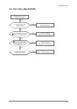
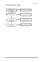
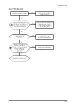
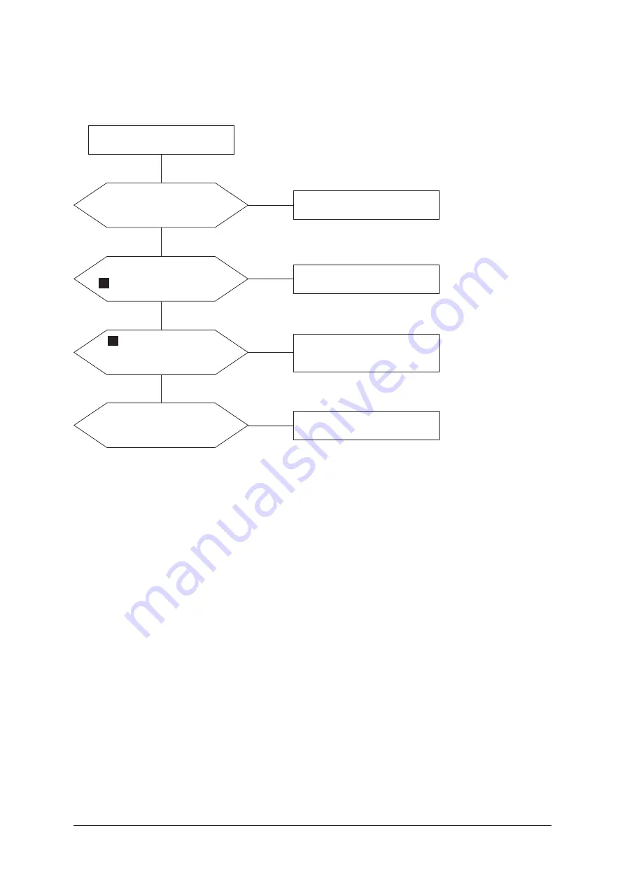
4-2-3 No Video (Digital-HDMI)

Check the connection

of HDMI cable?

Input a HDMI cable.

Yes

Does the digital data appear at

R1333_UX~R1340_UX?

Check a a IC1405

Change a main PCB ass'y.

Yes

Does the digital data

appear at output of  IC4001

LVDS(RA2008~2013)?

Check a IC1405

Change a main PCB ass'y.

Yes

Check a LVDS cable?

Replace lcd panel?

Please, Call to Samsung Co. LTD.

Yes

Power Indicator is off.

Lamp on, no video.

No

No

No

No

3

2

Summary of Contents for LE40N87BDX

Page 1: ...EN GTU46HEN GTU52SEN Model LE37M86BDX LE40M86BDX LE46M86BDX LE52M86BDX LE40N87BDX LE46N87BDX Manual SERVICE TFT LCD TV Fashion Feature Luxurious Slim Design Supreme Picture Quality Supreme Sound Quali...

Page 2: ...CX LE40N87BDX LE40M86BCX LE46M86BDX LE46M86BCX LE52M86BDX LE52M86BCX Service Manual First edition June 2007 Printed in Korea Trademarks Samsung is the registered trademark of Samsung Electronics Co Lt...

Page 3: ...Instruction 3 1 3 2 How to Access Service Mode 3 2 3 3 Factory Data 3 3 3 4 Service Adjustment 3 12 3 5 Servicing Information 3 15 4 4 Trouble shooting 4 4 1 4 1 First Checklist for Troubleshooting 4...

Page 4: ...the Wall Mount Kit 10 5 1 11 Disassembly and Reassembly 1 11 1 11 1 Disassembly 11 1 11 2 Reassembly 11 5 1 12 PCB Diagram 1 12 1 12 1 Main PCB Layout 12 1 12 2 IP Board Diagram 37 12 2 12 3 IP Board...

Page 5: ...City Gyeonggi Do Korea 443 742 Printed in Korea P N BN82 00191A 00 URL http itself sec samsung co kr This Service Manual is a property of Samsung Electronics Co Ltd Any unauthorized use of Manual can...

Page 6: ...Parametric EQ Connectivity 3 HDMI HDMI CEC Auto Wall Mount Set Position Control by Remote Control Best Picture Quality High Contrast Ratio High Clarity Anti Reflection Movie Plus Film Judder Cancel f...

Page 7: ...speakerOut Right 10W Left 10W BASSControlRange 8dB 8dB TREBLEControlRange 8dB 8dB HeadphoneOut 10mWMAX OutputFrequency RF 80Hz 15kHz A V 80Hz 20kHz Sound Characteristic TV System EnvironmentalConsider...

Page 8: ...kerOut Right 10W Left 10W BASSControlRange 8dB 8dB TREBLEControlRange 8dB 8dB HeadphoneOut 10mWMAX OutputFrequency RF 80Hz 15kHz A V 80Hz 20kHz Sound Characteristic TV System EnvironmentalConsideratio...

Page 9: ...75 Antenna Input MAXInternalspeakerOut Right 10W Left 10W BASSControlRange 8dB 8dB TREBLEControlRange 8dB 8dB HeadphoneOut 10mWMAX OutputFrequency RF 80Hz 15kHz A V 80Hz 20kHz Sound Characteristic TV...

Page 10: ...akerOut Right 10W Left 10W BASSControlRange 8dB 8dB TREBLEControlRange 8dB 8dB HeadphoneOut 10mWMAX OutputFrequency RF 80Hz 15kHz A V 80Hz 20kHz Sound Characteristic TV System EnvironmentalConsiderati...

Page 11: ...52M86BCX Model Design Frequency Horizontal Vertical Display Color 30 61 kHz 56 75 Hz 16 7 M colours PC Resolution Maximum mode Input Signal Sync Signal Video Signal Power Consumption Normal Power Savi...

Page 12: ...ification Item Item Name Remote Control Batteries AAA x 2 Power Cord Cover Bottom Stand Screw X 4 BN59 00603A 3903 000145 37 40 BN63 03031B 46 52 BN63 03148B Code No Remark Stand 37 40 BN90 001168A 46...

Page 13: ...2 Product Specifications 2 8 Memo...

Page 14: ...1 5 Exploded View and Parts List You can search for updated part codes through ITSELF web site URL http itself sec samsung co kr 5 1 LE37M86BDX LE37M86BCX Exploded View T0003 M0215 M0146 T0447 M0146 M...

Page 15: ...S 1 S A T0175 BN96 04771A ASSY SPEAKER P 8ohm 4pin Enclosure Type 1 S A T0447 BN96 04680C ASSY BRACKET P PANEL 37M87 AUO NT PAL 1 S N A M0215 BN07 00398A LCD PANEL T370HW02 8bit 37inch 16 7M 16 1 S A...

Page 16: ...5 Exploded View Parts List 5 3 5 3 LE40N87BDX Exploded View T0003 M0215 T0175 T0101 T0514 M0014 M0174 M0013 M0013 T0212...

Page 17: ...A T0175 BN96 04958A ASSY SPEAKER P 8ohm Tulip side side type 1 S A T0447 BN96 05213D ASSY BRACKET P PANEL 40N87 EO 1 S N A M0215 BN07 00409A LCD PANEL LTA400HT L01 8bit 40inch 16 7M 1 S A M0014 BN94...

Page 18: ...5 Exploded View Parts List 5 5 5 5 LE46M86BDX LE46M86BCX Exploded View T0003 M0215 T0447 M0014 M0013 M0107 T0275 M0027 M0146 T0175...

Page 19: ...V ABS PM 1 S A T0175 BN96 04771A ASSY SPEAKER P 8ohm 4pin Enclosure Type 1 S A T0447 BN96 05214B ASSY BRACKET P PANEL 46M81 EO 1 S N A M0215 BN07 00391A LCD PANEL LTA460HT LH2 10bit 46inch 1 0 1 S A M...

Page 20: ...5 Exploded View Parts List 5 7 5 7 LE52M86BDX LE52M86BCX Exploded View T0003 M0215 M0146 M0107 M0014 M0013 T0275 M0027 T0447 T0175...

Page 21: ...PM 1 S N A T0175 BN96 04772A ASSY SPEAKER P 8ohm 4pin Enclosure Type 1 S A T0447 BN96 05294A ASSY BRACKET P PANEL 52M81 UO EO SO LO 1 S N A M0215 BN07 00394A LCD PANEL LTA520HA03 10bit 52inch 1 07B 1...

Page 22: ...9 Schematic Diagrams 9 1 9 Schematic Diagrams This Document can not be used without Samsung s authorization 9 1 Stand by Power Schematic Diagram...

Page 23: ...9 Schematic Diagrams 9 2 This Document can not be used without Samsung s authorization 9 2 Sound Processing Schematic Diagram...

Page 24: ...9 Schematic Diagrams 9 3 This Document can not be used without Samsung s authorization 9 3 Input Output Jack I Schematic Diagram...

Page 25: ...9 Schematic Diagrams 9 4 This Document can not be used without Samsung s authorization 9 4 Input Output Jack II Schematic Diagram...

Page 26: ...9 Schematic Diagrams 9 5 This Document can not be used without Samsung s authorization 9 5 MICOM Schematic Diagram...

Page 27: ...9 Schematic Diagrams 9 6 This Document can not be used without Samsung s authorization 9 6 SVP UX Schematic Diagram...

Page 28: ...9 Schematic Diagrams 9 7 This Document can not be used without Samsung s authorization 9 7 DDR Tuner Schematic Diagram...

Page 29: ...9 Schematic Diagrams 9 8 This Document can not be used without Samsung s authorization 9 8 DTV Reset AV out Schematic Diagram...

Page 30: ...9 Schematic Diagrams 9 9 This Document can not be used without Samsung s authorization 9 9 DTV Memory STi5105 Schematic Diagram...

Page 31: ...9 Schematic Diagrams 9 10 This Document can not be used without Samsung s authorization 9 7 PCMCIA STi5105 Schematic Diagram...

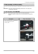
Page 32: ...tains electrostatically sensitive devices Use caution when handling these components 11 1 Disassembly LE37M86BDX Cautions 1 Disconnect the monitor from the power source before disassembly 2 Follow the...

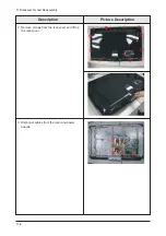
Page 33: ...11 Disassembly and Reassembly 11 2 3 Disconnet cables from the main and power boards Description Picture Description 2 Remove screws from the rear cover and lift up the rear cover...

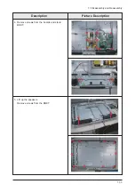
Page 34: ...11 Disassembly and Reassembly 11 3 5 Lift up the speakers Remove screws from the BRKT Description Picture Description 4 Remove screws from the boards and stand BRKT...

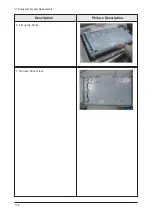
Page 35: ...11 Disassembly and Reassembly 11 4 7 Remove Panel Front Description Picture Description 6 Lift up the Panel...

Page 36: ...11 Disassembly and Reassembly 11 5 11 2 Reassembly Reassembly procedures are in the reverse order of disassembly procedures...

Page 37: ...11 Disassembly and Reassembly 11 6 Memo...

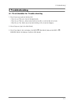
Page 38: ...burnt or damaged cable Check to see if there is a disconnected cable connection or a connection is too loose Check to see if the cables are connected according to the connection diagram 2 Check the po...

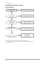
Page 39: ...ange a main PCB ass y Yes No Does proper DC 5V 3 3V 1 2V appear at C1153 C1178 C1170 Check a IC1111 IC1102 IC1113 Change a main PCB ass y Yes A power is supplied to set Check a other function No pictu...

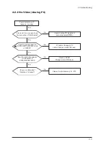
Page 40: ...Yes Does the signal appear at C2078 C2077 C2079 R G B of IC2001 PC cable Change a PC cable Change a main PCB ass y Yes Power Indicator is off Lamp on no video No No 1 Does the digital data appear at...

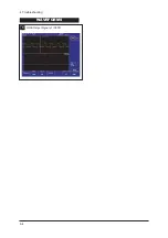
Page 41: ...4 Troubleshooting 4 4 WAVEFORMS 1 R G B Output Signal of IC2001...

Page 42: ...gital data appear at R1333_UX R1340_UX Check a a IC1405 Change a main PCB ass y Yes Does the digital data appear at output of IC4001 LVDS RA2008 2013 Check a IC1405 Change a main PCB ass y Yes Check a...

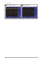
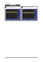
Page 43: ...4 Troubleshooting 4 6 2 Digital Output Data of IC4001 3 Signal of HDMI Data...

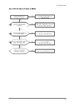
Page 44: ...Does the signal appear at C2085 of IC2001 Change a main PCB ass y Yes Does the digital data appear at output of RA2008 2013 Check a IC4001 Change a main PCB ass y Yes Power Indicator is off Lamp on no...

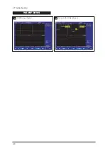
Page 45: ...4 Troubleshooting 4 8 WAVEFORMS 4 Tuner_CVBS Output Signal 3 CVBS Output Signal...

Page 46: ...Check a connection harness Yes Does the signal appear at Out of IC2001 RA2008 RA2013 Check a IC 2001 Change a main PCB ass y Yes Power Indicator is off Lamp on no picture No Check a A V cable and vid...

Page 47: ...4 Troubleshooting 4 10 WAVEFORMS 4 CVBS Output Signal...

Page 48: ...connection harness Yes Yes Power Indicator is off Lamp on no picure No Connect the s video cable Operating a video player No Does the digital data appear at Output of IC 2001 RA2008 RA2013 Check a IC...

Page 49: ...4 Troubleshooting 4 12 2 Digital Output Data of IC2001 5 Analog Signal Y C to IC2001 WAVEFORMS...

Page 50: ...nd Processor IC1202 SGTV5810 Yes Yes No Check the DC 12V of IC1203 Check a B12V Line Change a main PCB ass y Yes No Does the signal appear at Pin 47 or 48 53 or 54 CH1_L R Sound And Pin 36 or 37 30 or...

Page 51: ...4 Troubleshooting 4 14 WAVEFORMS 6 The Signal are Inputed to IC1202 7 The Signal are Inputed to IC1203...

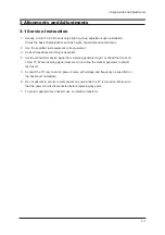
Page 52: ...ing is essential 4 Avoid overload Excessive signal from a sweep generator might overload the front end of the TV When inserting signal markers do not allow the marker generator to distort test result...

Page 53: ...Right Menu Enter Number Key 0 9 2 Function Control Key Power CH CH VOL VOL Menu TV VIDEO Enter 3 2 2 Panel Check You have to check Panel Maker Because of different adjustments as follows First of all...

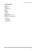
Page 54: ...n Block 6 SGTV5810 NTP3000 7 YC Delay 8 Adjust 9 I2C Check 10 W B MOVIE 11 Checksum 12 Reset 13 Spread Spectrum T TLPMPEUD xxxx Main Micom Ver T BDPMPEUS xxxx BORD2_CALLA_TR xxxx Sub Micom Ver Month D...

Page 55: ...er On Volume Max Volume Local Key Lock Power On Source Shop Mode Color Space PC Ident Language Ch Table TTX Group Nordic ON OFF 23 26 32 AMLCD_INT SAMSUNG ETRON 37 AU FHD BDP TLP Jasmine ON OFF ON OFF...

Page 56: ...Sl2Gain Sl4Gain Peakth1 Peakth2 Peskth3 Range 00 1FH 00 1FH 00 1FH 00 1FH 00 1FH 00 1FH 00 1FH 00 1FH 00H FFH 00H FFH 00H FFH RF 05H 04H 0CH 0CH 00H 00H 00H 00H 06H 2FH 3FH AV 05H 0AH 0CH 10H 00H 02H...

Page 57: ...10H 10H 01H DCH EBH DCH EBH 02H 02H 04H 0AH low high Delta No Item Range 1 2 3 4 5 6 7 8 9 10 11 12 13 TCD3 Contrast TCD3 Brightness TCD3 CR TCD3 CB TCD3 Delay Analog Y Offset Analog PB Offset Analog...

Page 58: ...FFH 00H FFH 00H FFH Reddish 00H 00H 00H No Item Range 1 2 3 4 5 6 7 8 9 10 11 12 13 14 15 16 OUTCON GAMMA OCC_MODE FALLBACK DBG_MARK SPR_CBR BIT_EXPAND INV_BIT_EXPAND REPEAT_MODE DEMO_ON_OFF MMU_RD_ST...

Page 59: ...20 120 56 128 128 15 30 130 1 165 140 128 128 115 128 128 128 128 0 1 44 20 120 128 20 40 100 200 56 128 128 15 30 130 1 165 140 128 128 128 128 128 128 128 0 1 44 20 120 128 20 40 100 200 56 128 128...

Page 60: ...5810 NTP3000 No Item Range 1 2 3 4 5 6 7 ID Tone Shift ID Tone Thresh Demod Prescaler Master Volume PWM Modulation DRC Threshold Speaker EQ 1H FH 00H FFH 00H 20H 00H 30H 80H F2H 00H 7FH ON OFF 01H 7FH...

Page 61: ...Level Magazine LNA PixelShift Test Debug ACR D Watchdog UART Select FBE select Tuner Tuner Top Semco Tuner Top Alps D Gamma M Gamma MJC PDP FRC 0 255 ON OFF ON OFF ON OFF 0 255 0 255 0 255 0 255 ON O...

Page 62: ...ie Color Movie Sharp ON OFF Movie 0 255 0 255 0 255 0 255 0 255 0 255 0 255 0 255 0 255 0 255 0 255 0 255 0 255 0 255 0 255 0 255 0 255 0 255 0 100 0 100 0 100 0 100 No Item Range OFF Movie Cool1 128...

Page 63: ...Adjustment If picture color is wrong check White Balance condition Equipment CA210 Patten Flat W B Pattern Adjust W B in Factory Mode Sub brightness and R G B Offset controls low light region Sub con...

Page 64: ...input to the mode in which the adjustment will be made RF DTV PC DVI Input signal VIDEO Mode Model 2 744 484 Mode Pattern 16 DTV DVI Mode Model 6 1280 720 Mode Pattern 16 HDMI Mode Model 6 1280 720 Mo...

Page 65: ...ust the high light Refer to table 1 2 in adjustment position by mode Adjust red gain x and blue gain y to the color coordinates Do not adjust the green gain and sub contrast Y data Picture 4 3 Flat W...

Page 66: ...grade 3 5 1 How to Update Flash ROM 1 Install the Flash Downloader ConnectSet Service Jack and Jig Cable to execute Program Update 2 Flash Downloader program update Before Turning on the set Click con...

Page 67: ...3 Alignments and Adjustments 3 16 Memo...

Page 68: ...7 Block Diagrams 7 1 7 Block Diagram This Document can not be used without Samsung s authorization...

Page 69: ...7 Block Diagrams 7 2 Memo...

Page 70: ...Diagram 12 1 Main PCB Layout CN2201_LCD CN3001_Test CN2203_FHD CN1101 Sound Processor HDMI Swich Tuner SVP WX IC Video Processor CN2001_Test Main Micro Processor Sub Micro Processor Test1801_Test DTV...

Page 71: ...12 PCB Diagram 12 2 12 2 IP Board Diagram 37...

Page 72: ...12 PCB Diagram 12 3 12 3 IP Board Diagram 40...

Page 73: ...12 PCB Diagram 12 4 12 4 IP Board Diagram 46...

Page 74: ...12 PCB Diagram 12 5 12 5 IP Board Diagram 52...

Page 75: ...12 PCB Diagram 12 6 Memo...

Page 76: ...DD_TX2 ODD_TX1 ODD_TX0 GND GND PANEL_VCC PANEL_VCC 1 2 3 4 5 SW_INVERTER ANA_DIM PWM_DIM GND SWNSOR POWER 1 2 3 4 R R L L 1 2 3 4 5 6 7 8 9 10 IR GND A5V_1 LED_STB BUZZER KEY_INPUT1 KEY_INPUT2 GND B5V...

Page 77: ...185 SGTV 5810 SDP64 FBE NTP 3000 DDR ADC HDMI3 S VIDEO S VIDEO HEADPHONE AV1 CN2201_LCD CN3001_TEST 10PIN CN3001_TEST TEST1801_TEST POWER SUPPLY CN1101_LCD CN2202_HD CN2203_FHD CN1606 10PIN CN1203 4PI...

Page 78: ...B12VS B12VS GND GND POWER PIN 17 18 19 20 21 22 23 24 25 26 27 28 29 30 31 32 NAME GND GND B5V B5V B5V B5V GND GND GND GND B12V B12V B12V B12V GND GND Function Define B12V B12V_CHN B9V B8V B5V_VCCT B5...

Page 79: ...A5V Front control board poewr supply KEY INPUT1 2 Key control from the memu change up down Etc IR Remote control signal LED Control the timing and stand by LED color CN505 Panel control PIN 1 2 3 4 5...

Page 80: ...VDD 17 TXOUTO1 3 VDD 18 TXOUTO1 4 VDD 19 TXOUTIO0 5 VDD 20 TXOUTO0 6 GND 21 TXOUTE3 7 GND 22 TXOUTE3 8 GND 23 TXOUTEC 9 GND 24 TXOUTEC 10 LVDS OPTION 25 TXOUTE2 11 TXOUTO3 26 TXOUTE2 12 TXOUTO3 27 TXO...

Page 81: ...8 Wiring Diagrams 8 6 8 4 Power Board Layout...

Page 82: ...1 2 3 4 5 6 7 8 9 10 11 12 13 14 15 16 NAME 13V GND 5 4V 5 4V 5 4V GND GND GND 12V 12V 12V GND GND GND ST7V PWR Functing Define ST7V Stand By Output PWR Power On Off Control Refer to CN801 function de...

Page 83: ...MLCD Panel Inverter Power 24V LAMP INVERTER Voltage B L Brightness sensor power A_D ANA_DIMMING P_D PWM_DIMMING CN803 Inverter power supply PIN 1 2 3 4 5 6 7 8 9 10 11 12 13 14 NAME 24V 24V 24V 24V 24...

Page 84: ...8 9 8 Wiring Diagrams...

Page 85: ...1 2 3 4 5 6 7 8 9 10 11 12 13 14 15 16 NAME 13V GND 5 4V 5 4V 5 4V GND GND GND 12V 12V 12V GND GND GND ST7V PWR Functing Define ST7V Stand By Output PWR Power On Off Control Refer to CN801 function d...

Page 86: ...Define AMLCD Panel Inverter Power 24V LAMP INVERTER Voltage B L Brightness sensor power A_D ANA_DIMMING P_D PWM_DIMMING CN804 Inverter power supply PIN 1 2 3 4 5 6 7 8 9 10 11 12 13 14 NAME 24V 24V 2...

Page 87: ...8 Wiring Diagrams 8 12 Memo...

Page 88: ...73 00052A RUBBER FOOT ARES 17 SILICON DIA 17 T1 6 S N A 0 1 BN91 01403A ASSY LCD AMLCD LNT4061FX 1 S N A 2 M0215 BN07 00409A LCD PANEL LTA400HT L01 8bit 40inch 16 7M 1 S A 0 1 BN91 01571B ASSY SHIELD...

Page 89: ...5P 1R 2mm STRA 1 S A 3 CN330 3711 004484 HEADER BOARD TO CABLE BOX 5P 1R 2mm STRA 1 S A 3 CN330 3711 004531 HEADER BOARD TO CABLE BOX 10P 1R 2mm ANG 1 S A 3 CN330 3711 005842 HEADER BOARD TO CABLE BOX...

Page 90: ...56 DIODE SWITCHING MMBD4148SE 100V 200mA SO 1 S A 4 D1492_NSID 0401 001056 DIODE SWITCHING MMBD4148SE 100V 200mA SO 1 S A 4 D1493_NSID 0401 001056 DIODE SWITCHING MMBD4148SE 100V 200mA SO 1 S A 4 D149...

Page 91: ...MD 1 S A 4 D1406 0406 001172 DIODE TVS CDS3C30GTH 48V SMD 1 S A 4 D1408 0406 001172 DIODE TVS CDS3C30GTH 48V SMD 1 S A 4 D1409 0406 001172 DIODE TVS CDS3C30GTH 48V SMD 1 S A 4 D1422 0406 001172 DIODE...

Page 92: ...0 1 S A 4 Q409 0505 000110 FET SILICON 2N7002 N 60V 115mA 7 5ohm 0 1 S A 4 Q409 0505 000110 FET SILICON 2N7002 N 60V 115mA 7 5ohm 0 1 S A 4 Q409 0505 000110 FET SILICON 2N7002 N 60V 115mA 7 5ohm 0 1...

Page 93: ...ISTOR 24Vdc 1 6x0 8x0 36mm TP 1 S A 4 R1527 2007 000042 R CHIP 499ohm 1 1 10W TP 1608 1 S A 4 R2139 2007 000043 R CHIP 1Kohm 1 1 10W TP 1608 1 S A 4 R2226 2007 000043 R CHIP 1Kohm 1 1 10W TP 1608 1 S...

Page 94: ...000070 R CHIP 0ohm 5 1 10W TP 1608 1 S A 4 R1826 2007 000070 R CHIP 0ohm 5 1 10W TP 1608 1 S A 4 R1827 2007 000070 R CHIP 0ohm 5 1 10W TP 1608 1 S A 4 R1828 2007 000070 R CHIP 0ohm 5 1 10W TP 1608 1...

Page 95: ...1 S A 4 R2379_FBE 2007 000070 R CHIP 0ohm 5 1 10W TP 1608 1 S A 4 R2380_FBE 2007 000070 R CHIP 0ohm 5 1 10W TP 1608 1 S A 4 R3013 2007 000070 R CHIP 0ohm 5 1 10W TP 1608 1 S A 4 R3018 2007 000070 R C...

Page 96: ...47ohm 5 1 10W TP 1608 1 S A 4 R1450 2007 000072 R CHIP 47ohm 5 1 10W TP 1608 1 S A 4 R1452 2007 000072 R CHIP 47ohm 5 1 10W TP 1608 1 S A 4 R1460 2007 000072 R CHIP 47ohm 5 1 10W TP 1608 1 S A 4 R1461...

Page 97: ...0W TP 1608 1 S A 4 R1843 2007 000074 R CHIP 100ohm 5 1 10W TP 1608 1 S A 4 R1855 2007 000074 R CHIP 100ohm 5 1 10W TP 1608 1 S A 4 R1856 2007 000074 R CHIP 100ohm 5 1 10W TP 1608 1 S A 4 R1858 2007 00...

Page 98: ...30ohm 5 1 10W TP 1608 1 S A 4 R1583 2007 000076 R CHIP 330ohm 5 1 10W TP 1608 1 S A 4 R1604_EU 2007 000076 R CHIP 330ohm 5 1 10W TP 1608 1 S A 4 R1607_EU 2007 000076 R CHIP 330ohm 5 1 10W TP 1608 1 S...

Page 99: ...W TP 1608 1 S A 4 R1256 2007 000084 R CHIP 4 7Kohm 5 1 10W TP 1608 1 S A 4 R1257 2007 000084 R CHIP 4 7Kohm 5 1 10W TP 1608 1 S A 4 R1308_WX 2007 000084 R CHIP 4 7Kohm 5 1 10W TP 1608 1 S A 4 R1351_WX...

Page 100: ...007 000084 R CHIP 4 7Kohm 5 1 10W TP 1608 1 S A 4 R3246 2007 000084 R CHIP 4 7Kohm 5 1 10W TP 1608 1 S A 4 R3268 2007 000084 R CHIP 4 7Kohm 5 1 10W TP 1608 1 S A 4 R1114 2007 000086 R CHIP 5 6Kohm 5 1...

Page 101: ...CHIP 10Kohm 5 1 10W TP 1608 1 S A 4 R3216 2007 000090 R CHIP 10Kohm 5 1 10W TP 1608 1 S A 4 R3217 2007 000090 R CHIP 10Kohm 5 1 10W TP 1608 1 S A 4 R3218 2007 000090 R CHIP 10Kohm 5 1 10W TP 1608 1 S...

Page 102: ...A 4 R2214 2007 000113 R CHIP 33ohm 5 1 10W TP 1608 1 S A 4 R2215 2007 000113 R CHIP 33ohm 5 1 10W TP 1608 1 S A 4 R2216 2007 000113 R CHIP 33ohm 5 1 10W TP 1608 1 S A 4 R2217 2007 000113 R CHIP 33ohm...

Page 103: ...4 R1428 2007 000309 R CHIP 10ohm 5 1 10W TP 1608 1 S A 4 R1429 2007 000309 R CHIP 10ohm 5 1 10W TP 1608 1 S A 4 R1430 2007 000309 R CHIP 10ohm 5 1 10W TP 1608 1 S A 4 R1431 2007 000309 R CHIP 10ohm 5...

Page 104: ...2007 000309 R CHIP 10ohm 5 1 10W TP 1608 1 S A 4 R2120_WX 2007 000309 R CHIP 10ohm 5 1 10W TP 1608 1 S A 4 R2121_WX 2007 000309 R CHIP 10ohm 5 1 10W TP 1608 1 S A 4 R2122_WX 2007 000309 R CHIP 10ohm...

Page 105: ...0W TP 1608 1 S A 4 R1670_EU 2007 001164 R CHIP 75ohm 1 1 10W TP 1608 1 S A 4 R1440 2007 001167 R CHIP 75ohm 5 1 10W TP 1608 1 S A 4 R1441 2007 001167 R CHIP 75ohm 5 1 10W TP 1608 1 S A 4 R1443 2007 00...

Page 106: ...8P TP 3 2x1 6 1 S A 4 RA2209_FBE 2011 001001 R NET 0ohm 5 1 16W L CHIP 8P TP 3 2x1 6 1 S A 4 RA2210_FBE 2011 001001 R NET 0ohm 5 1 16W L CHIP 8P TP 3 2x1 6 1 S A 4 RA2211_FBE 2011 001001 R NET 0ohm 5...

Page 107: ...08 1 S A 4 C1303 2203 000189 C CER CHIP 100nF 80 20 25V Y5V 1608 1 S A 4 C1313_WX 2203 000189 C CER CHIP 100nF 80 20 25V Y5V 1608 1 S A 4 C1319 2203 000189 C CER CHIP 100nF 80 20 25V Y5V 1608 1 S A 4...

Page 108: ...IP 100nF 10 25V X7R 2012 1 S A 4 C2217 2203 000221 C CER CHIP 100nF 20 50V Y5V TP 3216 1 S A 4 C1293 2203 000236 C CER CHIP 0 1nF 5 50V C0G 1608 1 S A 4 C1309 2203 000236 C CER CHIP 0 1nF 5 50V C0G 16...

Page 109: ...C CER CHIP 10nF 10 50V X7R 1608 1 S A 4 C2221 2203 000257 C CER CHIP 10nF 10 50V X7R 1608 1 S A 4 C2231 2203 000257 C CER CHIP 10nF 10 50V X7R 1608 1 S A 4 C2268_LCD 2203 000257 C CER CHIP 10nF 10 50...

Page 110: ...301_FBE 2203 000440 C CER CHIP 1nF 10 50V X7R 1608 1 S A 4 C1105 2203 000491 C CER CHIP 2 2nF 10 50V X7R 1608 1 S A 4 C2019 2203 000531 C CER CHIP 2 7nF 10 50V X7R 1608 1 S A 4 C2030 2203 000531 C CER...

Page 111: ...1 S A 4 C2134_WX 2203 000972 C CER CHIP 47nF 10 16V X7R 1608 1 S A 4 C2135_WX 2203 000972 C CER CHIP 47nF 10 16V X7R 1608 1 S A 4 C2136_WX 2203 000972 C CER CHIP 47nF 10 16V X7R 1608 1 S A 4 C2138_WX...

Page 112: ...10 16V X7R 1608 1 S A 4 C2028_WX 2203 005005 C CER CHIP 100nF 10 16V X7R 1608 1 S A 4 C2145_WX 2203 005005 C CER CHIP 100nF 10 16V X7R 1608 1 S A 4 C2146_WX 2203 005005 C CER CHIP 100nF 10 16V X7R 160...

Page 113: ...0nF 10 16V X7R 1608 1 S A 4 C3138 2203 005005 C CER CHIP 100nF 10 16V X7R 1608 1 S A 4 C3139 2203 005005 C CER CHIP 100nF 10 16V X7R 1608 1 S A 4 C3140 2203 005005 C CER CHIP 100nF 10 16V X7R 1608 1 S...

Page 114: ...V Y5V 1608 1 S A 4 C2022 2203 005065 C CER CHIP 1000nF 80 20 10V Y5V 1608 1 S A 4 C2023 2203 005065 C CER CHIP 1000nF 80 20 10V Y5V 1608 1 S A 4 C2024 2203 005065 C CER CHIP 1000nF 80 20 10V Y5V 1608...

Page 115: ...10 10V X5R 2012 1 S A 4 C1212 2203 006361 C CER CHIP 10000nF 10 10V X5R 2012 1 S A 4 C1213 2203 006361 C CER CHIP 10000nF 10 10V X5R 2012 1 S A 4 C1228 2203 006361 C CER CHIP 10000nF 10 10V X5R 2012 1...

Page 116: ...X5R 2012 1 S A 4 C3007 2203 006361 C CER CHIP 10000nF 10 10V X5R 2012 1 S A 4 C3008 2203 006361 C CER CHIP 10000nF 10 10V X5R 2012 1 S A 4 C3015 2203 006361 C CER CHIP 10000nF 10 10V X5R 2012 1 S A 4...

Page 117: ...20 12x12mm 1 S A 4 T0052 2703 002722 INDUCTOR SMD 22uH 20 12x12mm 1 S A 4 L1201 2704 000018 INDUCTOR SMD ARRAY 15uH 2000mA 2 0 124oh 1 S N A 4 L1202 2704 000018 INDUCTOR SMD ARRAY 15uH 2000mA 2 0 124o...

Page 118: ...HM 30MHz 1 S A 4 T0568 3301 001404 BEAD SMD 30ohm 2012 TP 15 9OHM 30MHz 1 S A 4 T0568 3301 001404 BEAD SMD 30ohm 2012 TP 15 9OHM 30MHz 1 S A 4 T0568 3301 001404 BEAD SMD 30ohm 2012 TP 15 9OHM 30MHz 1...

Page 119: ...ASSY LABEL LE40N86BDX 1 S N A 0 1 M0001 BN90 01251D ASSY COVER FRONT 40N87 EO 1 S N A 2 T0175 BN96 04958A ASSY SPEAKER P 8ohm Tulip side side type 1 S A 2 T0003 BN96 05067D ASSY COVER P FRONT 40N87 E...

Page 120: ...ion Mosel consists of three main blocks 1 Main board Video signal processing 2 IP board Power supply Inverter 3 T con board LCD Panel control RF IN Air Cable Scart 1 2 A V S Video Component HDMI 1 2 P...

Page 121: ...sists of three main blocks 1 Main board Video signal processing 2 SMPS Power supply 3 T con board LCD Panel control SMPS INVERTER RF IN Scart 1 2 A V S Video Component HDMI 1 2 Main Board Panel T con...

Page 122: ...13 Circuit Descriptions 13 3 13 2 Main Block...

Page 123: ...13 Circuit Descriptions 13 4 13 3 IP Board...

Page 124: ...rs 3 Press to decrease or increase the volume In the on screen menu use the buttons as you use the and buttons on the remote control 4 C P Press to change channels In the on screen menu use the C P bu...

Page 125: ...x VCR or DVD Inputs or outputs for external devices such as VCR DVD video game device or video disc players 2 Connecting AUDIO Connect RCA audio cables to R AUDIO L on the rear of your set and the oth...

Page 126: ...ing an Aerial or Cable Television Network To view television channels correctly a signal must be received by the set from one of the following sources An outdoor aerial A cable television network A sa...

Page 127: ...and Y connectors on your component devices DTV or DVD are sometimes labeled Y B Y and R Y or Y Cb and Cr Connect RCA audio cables optional to R AUDIO L on the rear of your set and the other ends to co...

Page 128: ...Available source selection 19 Previous channel 20 DTV menu display 21 Records for Live Broadcasting 22 P Next channel P Previous channel 23 Exit the OSD 24 Control the cursor in the menu 25 Use to se...

Page 129: ...10 Operating Instructions and Installation 10 6 Memo...

Page 130: ...d Coarse FINE Fine adjustment is used to adjust visibility by control phase difference COARSE This is a adjustment by tuning with Video colck and PLL clock DVI Digital Visual Interface This provides a...

Page 131: ...ace method while showing odd lines and then even lines in turn is called the Interlace method The Non Interlace method is used for the majority of monitors to ensure a clear image The Interlace method...

Page 132: ...cational programs Different from cable TV CATV can be viewed only within the area in which the CATV service is offered S Video Short for Super Video S Video allows up to 800 lines of horizontal resolu...

Page 133: ...Assignments NC DDC Input power 5V IDENT DVI Output Signal HDCP Control Rx0 Rx0 GND NC NC GND RxC RxC 13 14 15 16 17 18 19 20 21 22 23 24 1 2 3 4 5 6 7 8 9 10 11 12 Rx2 Rx2 GND NC NC DDC SCL DDC SDA NC...

Page 134: ...3 4 5 6 7 8 9 10 11 12 13 14 15 Red Green Blue GND GND GND Red GND Green GND Blue DDC Input power 5V IDENT PC GND DDC Data SDA H SYNC V SYNC DDC Clock SCL 14 2 5 D SUB 14 2 2 Component RCA White RCA...

Page 135: ...input 16 Fast Blanking signal RGB switching 17 Video output GND 18 Video input GND 19 Video output CVBS out 20 Video input CVBS in 21 Common GND Pin Signal 1 Audio output R 2 Audio input R 3 Audio ou...

Page 136: ...nce Infomation 14 7 14 3 Timing Chart This section of the service manual describes the timing that the computer industry recognizes as standard for computer generated video signals 14 3 1 LCD Panel Mo...

Page 137: ...14 Reference Infomation 14 8 14 3 2 Supported Modes 1...

Page 138: ...14 Reference Infomation 14 9 14 3 3 Supported Modes 2...

Page 139: ...14 Reference Infomation 14 10 14 3 4 Supported Modes 3...

Page 140: ...of 17 EH L05 SEC LTM170E5 L03 BN07 00056A ED Dell 1702FP pro E4 EH mechanical Compatible SEC LTM190E1 L01 BN07 00057A EE DELL 1900 FP SEC LTM181E5 L01 BN07 00061A EF 18 narrow bezel GH18PS SEC LTM150...

Page 141: ...LTM190E1 L03 BN07 00151A E15 Development new 19 Panel form AMLCD Panel only for TCO03 SEC LTM240W1 L03 BN07 00134A E16 AMLCD 24 panel development SEC LTM190E1 L02 BN07 00128B E17 New Panel from AMLCD...

Page 142: ...C LTA320WS LH2 BN07 00244A SPZ AMLCD 32 16 9 SPVA 90 new Panel SEC LTA400WS LH1 BN07 00245A SPZ AMLCD 40 16 9 SPVA 90 new Panel SEC LTM190M2 L01 BN07 00227A STZ AMLCD 19 TN Wide new Panel Code develop...

Page 143: ...10 BN07 00090A RJ L10 NORMAL TORISAN TM190SX 70N01 BN07 00098A RK Torisan 19 Panel TORISAN TM181SX 76N01 BN07 00106A RL ZPD Panel code TORISAN TM190SX 70N01 BN07 00107A RM ZPD Panel code TORISAN TM290...

Page 144: ...evelopment ACER M170EN06 BN07 00171B ATZ AU Monitor 17 ZPD code derivation ACER T315XW01 BN07 00194A AMZ AU 32 new ACER M170EG01 BN07 00192A ATH AU TN PSWG type new Panel code ACER M170EG01 BN07 00192...

Page 145: ...IMEI M170E6 L05 BN07 00152B CS CMO 17 ZPD panel code derivation CHIMEI M150X4 L06 BN07 00137B CT Chimei 15 Narrow Slim panel ZPD derivation CHIMEI M170E5 L05 BN07 00165A CTH CMO 17 new panel developme...

Page 146: ...D On Screen Display On screen display customer can control the screen easily with this Image Lock This means Fineness adjustment in LCD Monitor the features are Fine and Coarse FINE Fine adjustment is...

Page 147: ...eck Figure 1 1 WARNING Do not use an isolation transformer during this test Use a leakage current tester or a metering system that complies with American National Standards Institute ANSI C101 1 Leaka...

Page 148: ...rd from the AC source and turn the power switch ON Connect an insulation resistance meter 500 V to the blades of the AC plug The insulation resistance between each blade of the AC plug and accessible...

Page 149: ...t may cause a fire or electric shock 5 Make sure to turn the power off and unplug the power cord from the outlet before repositioning the product Also check the antenna cable or the external connector...

Page 150: ...Memo 1 Precautions 1 4...

Page 151: ...w Parts List 5 1 5 Exploded View and Parts List You can search for updated part codes through ITSELF web site URL http itself sec samsung co kr 5 1 LE40N87BDX Exploded View T0003 T0175 M0215 T0447 M00...

Page 152: ...A T0175 AA68 03278B MANUAL FLYER 01 WARRANTY CARD CIS All mo 1 S N A T0447 BN96 05213D ASSY BRACKET P PANEL 40N87 EO 1 S N A M0215 BN07 00409A LCD PANEL LTA400HT L01 8bit 40inch 16 7M 1 S A M0014 BN94...

Page 153: ...5 Exploded View Parts List 5 3 5 3 LE46N87BDX Exploded View M0014 M0013 M0027 T0003 M0215 T0175...

Page 154: ...A T0175 BN96 04958B ASSY SPEAKER P 8ohm Tulip side 46 50 1 S A T0447 BN96 04641B ASSY BRACKET P PANEL TULIP SIDE 46 EO 1 S N A M0215 BN07 00410A LCD PANEL LTA460HT L01 8bit 46inch 16 7M 1 S A M0014 BN...

Page 155: ...9 Schematic Diagrams 9 1 9 Schematic Diagrams This Document can not be used without Samsung s authorization 9 1 Stand by Power Schematic Diagram...

Page 156: ...9 Schematic Diagrams 9 2 This Document can not be used without Samsung s authorization 9 2 Sound Processing Schematic Diagram...

Page 157: ...9 Schematic Diagrams 9 3 This Document can not be used without Samsung s authorization 9 3 Input Output Jack I Schematic Diagram...

Page 158: ...9 Schematic Diagrams 9 4 This Document can not be used without Samsung s authorization 9 4 Input Output Jack II Schematic Diagram...

Page 159: ...9 Schematic Diagrams 9 5 This Document can not be used without Samsung s authorization 9 5 MICOM Schematic Diagram...

Page 160: ...9 Schematic Diagrams 9 6 This Document can not be used without Samsung s authorization 9 6 SVP UX Schematic Diagram...

Page 161: ...9 Schematic Diagrams 9 7 This Document can not be used without Samsung s authorization 9 7 DDR Tuner Schematic Diagram...

Page 162: ...9 Schematic Diagrams 9 8 This Document can not be used without Samsung s authorization 9 8 DTV Reset AV out Schematic Diagram...

Page 163: ...9 Schematic Diagrams 9 9 This Document can not be used without Samsung s authorization 9 9 DTV Memory STi5105 Schematic Diagram...

Page 164: ...9 Schematic Diagrams 9 10 This Document can not be used without Samsung s authorization 9 7 PCMCIA STi5105 Schematic Diagram...

Page 165: ...Gray T1 5 6 S N A 0 1 BN91 01403A ASSY LCD AMLCD LNT4061FX 1 S N A 2 M0215 BN07 00409A LCD PANEL LTA400HT L01 8bit 40inch 16 7M 1 S A 0 1 BN91 01571B ASSY SHIELD SQE LE40N86BDX 1 S N A 2 M0081 6003 0...

Page 166: ...004531 HEADER BOARD TO CABLE BOX 10P 1R 2mm ANG 1 S A 3 CN330 3711 005842 HEADER BOARD TO CABLE BOX 24P 2R 2MM STR 1 S A 3 JA330 3722 000143 JACK PHONE 1P VER AG BLK ANGLE 1 S A 3 JA1601_EU 3722 00049...

Page 167: ...100V 200mA SO 1 S A 4 D1492_NSID 0401 001056 DIODE SWITCHING MMBD4148SE 100V 200mA SO 1 S A 4 D1493_NSID 0401 001056 DIODE SWITCHING MMBD4148SE 100V 200mA SO 1 S A 4 D1494_NSID 0401 001056 DIODE SWIT...

Page 168: ...72 DIODE TVS CDS3C30GTH 48V SMD 1 S A 4 D1447 0406 001172 DIODE TVS CDS3C30GTH 48V SMD 1 S A 4 D1601_OP 0406 001172 DIODE TVS CDS3C30GTH 48V SMD 1 S A 4 D1602_OP 0406 001172 DIODE TVS CDS3C30GTH 48V S...

Page 169: ...SILICON 2N7002 N 60V 115mA 7 5ohm 0 1 S A 4 Q409 0505 000110 FET SILICON 2N7002 N 60V 115mA 7 5ohm 0 1 S A 4 IC104 0801 002095 IC CMOS LOGIC 74LCX245 TRANSCEIVER TSSOP 1 S A 4 IC104 0801 002095 IC CM...

Page 170: ...0052 R CHIP 10Kohm 1 1 10W TP 1608 1 S A 4 R1906 2007 000052 R CHIP 10Kohm 1 1 10W TP 1608 1 S A 4 R1907 2007 000052 R CHIP 10Kohm 1 1 10W TP 1608 1 S A 4 R1908 2007 000052 R CHIP 10Kohm 1 1 10W TP 16...

Page 171: ...08 1 S A 4 R1838 2007 000070 R CHIP 0ohm 5 1 10W TP 1608 1 S A 4 R1839 2007 000070 R CHIP 0ohm 5 1 10W TP 1608 1 S A 4 R1840 2007 000070 R CHIP 0ohm 5 1 10W TP 1608 1 S A 4 R1844 2007 000070 R CHIP 0o...

Page 172: ...10W TP 1608 1 S A 4 R3128 2007 000070 R CHIP 0ohm 5 1 10W TP 1608 1 S A 4 R3129 2007 000070 R CHIP 0ohm 5 1 10W TP 1608 1 S A 4 R3130 2007 000070 R CHIP 0ohm 5 1 10W TP 1608 1 S A 4 R3133 2007 000070...

Page 173: ...222 2007 000074 R CHIP 100ohm 5 1 10W TP 1608 1 S A 4 R1225 2007 000074 R CHIP 100ohm 5 1 10W TP 1608 1 S A 4 R1226 2007 000074 R CHIP 100ohm 5 1 10W TP 1608 1 S A 4 R1228 2007 000074 R CHIP 100ohm 5...

Page 174: ...CHIP 100ohm 5 1 10W TP 1608 1 S A 4 R2123_WX 2007 000074 R CHIP 100ohm 5 1 10W TP 1608 1 S A 4 R2124_WX 2007 000074 R CHIP 100ohm 5 1 10W TP 1608 1 S A 4 R2203 2007 000074 R CHIP 100ohm 5 1 10W TP 16...

Page 175: ...4 R1691 2007 000077 R CHIP 470ohm 5 1 10W TP 1608 1 S A 4 R2052 2007 000077 R CHIP 470ohm 5 1 10W TP 1608 1 S A 4 R2246_LCD 2007 000077 R CHIP 470ohm 5 1 10W TP 1608 1 S A 4 R2287_LCD 2007 000077 R C...

Page 176: ...4 R1822_1M 2007 000084 R CHIP 4 7Kohm 5 1 10W TP 1608 1 S A 4 R1824 2007 000084 R CHIP 4 7Kohm 5 1 10W TP 1608 1 S A 4 R1825 2007 000084 R CHIP 4 7Kohm 5 1 10W TP 1608 1 S A 4 R1865 2007 000084 R CHIP...

Page 177: ...454 2007 000090 R CHIP 10Kohm 5 1 10W TP 1608 1 S A 4 R1457 2007 000090 R CHIP 10Kohm 5 1 10W TP 1608 1 S A 4 R1465 2007 000090 R CHIP 10Kohm 5 1 10W TP 1608 1 S A 4 R1466 2007 000090 R CHIP 10Kohm 5...

Page 178: ...47Kohm 5 1 10W TP 1608 1 S A 4 R1541 2007 000097 R CHIP 47Kohm 5 1 10W TP 1608 1 S A 4 R1614_EU 2007 000097 R CHIP 47Kohm 5 1 10W TP 1608 1 S A 4 R1615_EU 2007 000097 R CHIP 47Kohm 5 1 10W TP 1608 1 S...

Page 179: ...0W TP 1608 1 S A 4 R3242 2007 000113 R CHIP 33ohm 5 1 10W TP 1608 1 S A 4 R3245 2007 000113 R CHIP 33ohm 5 1 10W TP 1608 1 S A 4 R2148_WX 2007 000118 R CHIP 390ohm 5 1 10W TP 1608 1 S A 4 R1350 2007 0...

Page 180: ...TP 1608 1 S A 4 R1487 2007 000309 R CHIP 10ohm 5 1 10W TP 1608 1 S A 4 R1504_HDMI 2007 000309 R CHIP 10ohm 5 1 10W TP 1608 1 S A 4 R1506_HDMI 2007 000309 R CHIP 10ohm 5 1 10W TP 1608 1 S A 4 R1508_HDM...

Page 181: ...10W TP 1608 1 S A 4 R1246 2007 000882 R CHIP 4 7ohm 5 1 10W TP 1608 1 S A 4 R1247 2007 000882 R CHIP 4 7ohm 5 1 10W TP 1608 1 S A 4 R1249 2007 000882 R CHIP 4 7ohm 5 1 10W TP 1608 1 S A 4 R1251 2007...

Page 182: ...10ohm 5 1 16W L CHIP 8P TP 3216 1 S A 4 RA1807 2011 000651 R NET 10ohm 5 1 16W L CHIP 8P TP 3216 1 S A 4 RA1808 2011 000651 R NET 10ohm 5 1 16W L CHIP 8P TP 3216 1 S A 4 RA1809 2011 000651 R NET 10oh...

Page 183: ...011 001093 R NET 100OHM 5 1 16W L CHIP 8P TP 3216 1 S A 4 RA2006_WX 2011 001093 R NET 100OHM 5 1 16W L CHIP 8P TP 3216 1 S A 4 RA2007_WX 2011 001093 R NET 100OHM 5 1 16W L CHIP 8P TP 3216 1 S A 4 RA32...

Page 184: ...2203 000189 C CER CHIP 100nF 80 20 25V Y5V 1608 1 S A 4 C2074 2203 000189 C CER CHIP 100nF 80 20 25V Y5V 1608 1 S A 4 C2085 2203 000189 C CER CHIP 100nF 80 20 25V Y5V 1608 1 S A 4 C2086 2203 000189 C...

Page 185: ...1 S A 4 C1853 2203 000257 C CER CHIP 10nF 10 50V X7R 1608 1 S A 4 C2027 2203 000257 C CER CHIP 10nF 10 50V X7R 1608 1 S A 4 C2032 2203 000257 C CER CHIP 10nF 10 50V X7R 1608 1 S A 4 C2033 2203 000257...

Page 186: ...R CHIP 1nF 10 50V X7R 1608 1 S A 4 C1272 2203 000440 C CER CHIP 1nF 10 50V X7R 1608 1 S A 4 C1273 2203 000440 C CER CHIP 1nF 10 50V X7R 1608 1 S A 4 C1274 2203 000440 C CER CHIP 1nF 10 50V X7R 1608 1...

Page 187: ...36 2203 000888 C CER CHIP 4 7nF 10 50V X7R 1608 1 S A 4 C1257 2203 000888 C CER CHIP 4 7nF 10 50V X7R 1608 1 S A 4 C1258 2203 000888 C CER CHIP 4 7nF 10 50V X7R 1608 1 S A 4 C1259 2203 000888 C CER CH...

Page 188: ...C1153 2203 005005 C CER CHIP 100nF 10 16V X7R 1608 1 S A 4 C1154 2203 005005 C CER CHIP 100nF 10 16V X7R 1608 1 S A 4 C1157 2203 005005 C CER CHIP 100nF 10 16V X7R 1608 1 S A 4 C1159 2203 005005 C CE...

Page 189: ...R 1608 1 S A 4 C3111 2203 005005 C CER CHIP 100nF 10 16V X7R 1608 1 S A 4 C3112 2203 005005 C CER CHIP 100nF 10 16V X7R 1608 1 S A 4 C3113 2203 005005 C CER CHIP 100nF 10 16V X7R 1608 1 S A 4 C3114 22...

Page 190: ...218 2203 005005 C CER CHIP 100nF 10 16V X7R 1608 1 S A 4 C3219 2203 005005 C CER CHIP 100nF 10 16V X7R 1608 1 S A 4 C3220 2203 005005 C CER CHIP 100nF 10 16V X7R 1608 1 S A 4 C3221 2203 005005 C CER C...

Page 191: ...2 2203 005918 C CER CHIP 1000nF 10 6 3V X7R 1608 1 S A 4 C1223 2203 005918 C CER CHIP 1000nF 10 6 3V X7R 1608 1 S A 4 C1224 2203 005918 C CER CHIP 1000nF 10 6 3V X7R 1608 1 S A 4 C1225 2203 005918 C C...

Page 192: ...6361 C CER CHIP 10000nF 10 10V X5R 2012 1 S A 4 C1821 2203 006361 C CER CHIP 10000nF 10 10V X5R 2012 1 S A 4 C1822 2203 006361 C CER CHIP 10000nF 10 10V X5R 2012 1 S A 4 C1828 2203 006361 C CER CHIP 1...

Page 193: ...ORGANIC 82UF 20 6 3V WT TP 6 3 5 9MM 1 S A 4 C2099 2409 001051 C ORGANIC 82UF 20 6 3V WT TP 6 3 5 9MM 1 S A 4 T0052 2703 000125 INDUCTOR SMD 10uH 10 2012 1 S A 4 T0052 2703 000125 INDUCTOR SMD 10uH 1...

Page 194: ...TP 0 1ohm 1 S A 4 T0568 3301 001324 BEAD SMD 15ohm 2012 600mA TP 0 1ohm 1 S A 4 T0568 3301 001324 BEAD SMD 15ohm 2012 600mA TP 0 1ohm 1 S A 4 T0568 3301 001324 BEAD SMD 15ohm 2012 600mA TP 0 1ohm 1 S...

Page 195: ...ER BOTTOM TULIP SIDE 40 HIPS HB BK500 1 S A 0 1 M0003 BN92 02504C ASSY BOX TULIP SIDE 40 EO 1 S N A 2 M0521 BN69 01803A BOX SET IN 40N8 TULIPSIDE CB C1 DY 01 W 1 02 S N A 2 BN69 01804A BOX SET OUT 40N...

Page 196: ...GRILLE SPEAKER 40N8 PET SHEET T0 25 6 5 1 S N A 3 BN96 05079C ASSY DECORATION P 40N81 LEFT ABS HB V 1 S A 4 BN61 03261B BOSS TAPE Tulip ACRYL T1 1 W20mm GRAY TA 0 55 S N A 4 T0056 BN63 03297A COVER D...

Reviews: